EP0258671A2 - Architecture d'un canal de lecture pour le traitement des signaux d'une tête de lecture - Google Patents
Architecture d'un canal de lecture pour le traitement des signaux d'une tête de lecture Download PDFInfo
- Publication number
- EP0258671A2 EP0258671A2 EP87111371A EP87111371A EP0258671A2 EP 0258671 A2 EP0258671 A2 EP 0258671A2 EP 87111371 A EP87111371 A EP 87111371A EP 87111371 A EP87111371 A EP 87111371A EP 0258671 A2 EP0258671 A2 EP 0258671A2
- Authority
- EP
- European Patent Office
- Prior art keywords
- signal
- zero
- output
- waveform
- flip
- Prior art date
- Legal status (The legal status is an assumption and is not a legal conclusion. Google has not performed a legal analysis and makes no representation as to the accuracy of the status listed.)
- Withdrawn
Links
Images
Classifications
-
- G—PHYSICS
- G11—INFORMATION STORAGE
- G11B—INFORMATION STORAGE BASED ON RELATIVE MOVEMENT BETWEEN RECORD CARRIER AND TRANSDUCER
- G11B20/00—Signal processing not specific to the method of recording or reproducing; Circuits therefor
- G11B20/10—Digital recording or reproducing
- G11B20/10009—Improvement or modification of read or write signals
Definitions
- This invention relates generally to the retrieval of data recorded on magnetic media and deals more particularly with improved circuitry for processing electrical signals generated by a read head.
- the recording of data on magnetic media such as disks and tapes is normally carried out by entering the encoded data as a continuous track of magnetization having polarity reversals at intervals determined by the data that is being recorded and by the rules of the particular encoding and recording processes that are employed.
- the recorded data are recovered by sensing polarity reversals, i.e., the presence, absence and relative position of each change in polarity. It is only the polarity changes that are important, not the polarity itself.
- the polarity reversals are commonly referred to as flux transitions and are detected by using an inductive read head. When the magnetized track of data is moved past the sensitive gap of the read head, current is induced to flow and the read head thus generates a small voltage pulse each time an area of flux transition passes through the read head gap.
- the pulses which are thereby generated are amplified and converted by read channel circuitry into a binary signal suitable for use by data processing equipment.
- the read channel circuitry must be capable of performing this conversion in spite of numerous signal distortions and corruptions that can occur during both normal and abnormal operation of the equipment. Included among the problems that are often encountered is the loss of signal amplitude which can occur for a variety of reasons.
- two general approaches have been taken. One is to use. automatic gain control and the other involves designing the read channel circuit in a manner to be intrinsically insensitive to the amplitude of the signal. The need for automatic gain control adds to the cost and complexity of the circuitry, while amplitude insensitive circuits have problems of their own, as will be discussed more fully.
- the read channel circuitry typically includes one or more gain stages, a lowpass filter for attenuating unwanted frequencies, a differentiator for differentiating the signal, and a zero crossing detector.
- the circuit is arranged to detect the voltage peaks in the read channel's signal which correspond to flux transitions, and its performance is best at high flux densities, but has a serious shortcoming at the low flux densities of a given system. Whether the polarity is positive or negative is not important, and the amplitudes of the pulses are also ignored.
- the function of the differentiator is to convert the peaks, both positive and negative, to zero crossings, and the zero crossing detector is normally implemented with a conventional comparator which detects zero crossings of the differentiated signal.
- self clocking codes are usually used because they avoid the need for separate clock information to be recorded on a separate track or other separate FM, MFM, GCR and RLL code schemes.
- data and clock information are mixed together and recorded on the same track. Mixing of data and clock information together increases the flux density on the medium but not unduly if the self clocking code is well designed.
- FM code was used in the past but has now been supplanted by MFM code which is more efficient and perhaps the most widely used code at present.
- a newer class of codes referred to as RLL (run length limited) codes have recently evolved and exhibit efficiency improvement over MFM.
- the characteristics of the RLL codes are especially compatible with web-coated magnetic recording media and with state of the art electronic components.
- the efficiency gains of the RLL codes are achieved in part by broadening the bandwidth that is required to process the RLL signal in the read channel.
- the bandwidth is commonly expressed as the ratio of the highest frequency or flux-densities to the lowest frequency or flux-densities of the fundamental signals, and it has a significant impact on the read channel circuitry design.
- MFM has a relatively narrow bandwidth of 2:1, and this gives the differentiator little trouble.
- the greater 2.67:1 bandwidth of RLL noticeably worsens the performance of the differentiator, and the GCR bandwidth of 3:1 makes it worse yet.
- the reason for the problem is the "saddle" shape that the differentiated signal acquires as the spread between the lowest and highest frequencies Lncreases and the flux-transitions are spread farther apart in time.
- the middle or "notch" of the saddle" shaped signal can approach or even cross zero, especially when noise is considered, and it can then be interpreted as a flux transition when in fact it is not.
- the problem of spurious zero crossings in the signal is most acute with the more efficient codes such as RLL.
- One approach involves implementing two parallel filters for filtering of the signal.
- One filter is used as a high resolution filter which attenuates only the high frequency noise with little effect on the desired signal.
- the other filter is a low resolution filter which attenuates the portion of the signal at the high end of the signal's band width.
- the low resolution filter reduces the depth of the notch in each "saddle" portion of the differentiated signal by reducing the amplitude of the high frequency component which is superimposed on a low frequency component to create the "saddle” shape.
- the high resolution signal retains the system resolution and timing accuracy and is applied as a digitized clock signal to a type D flip flop which also receives the low resolution signal as its data input.
- the signal timing is dependent on the propagation delays of the two filters, among other things, and the propogation delay can vary substantially depending on the data involved and other variables.
- the dual filter system is subject to pattern sensitivity which detracts from its ability to give consistent results under the operating conditions it can be expected to encounter.
- comparators to detect the amplitude of the undifferentiated signal and logic gating which ignores false peaks by rejecting zero crossings in the differentiated signal that occur at the same time that the undifferentiated signal has an amplitude below the threshold of the comparators.
- This type of system is plagued by added cost and circuit complexity resulting from the need for the amplitude comparators and related components. Even more significantly, the system is amplitude sensitive and the whole system will fail if the amplitude drops below the comparator threshold for some reason. Therefore, accurate control of the signal amplitude is crucial, and it is usually necessary to include automatic gain control or similar circuitry in order for the system to operate successfully. The need for additional components to control the amplitude adds to the cost, complexity and space requirements of the read channel circuit. Even with automatic gain control, the system is not infallible.
- the present invention is directed to an improved read channel circuit in which the false peak problem is essentially eliminated without any significant sacrifice in reliability or cost.
- a single high resolution filter is used to filter out the high frequency noise from the read head signal.
- the filtered signal is then passed through two separate differentiator circuits, one of which is adjusted to be imperfect in its differentiation to thereby reduce the depth of the notch in the saddle shaped signal that results from differentiation. This imperfect differentiation displaces the false peaks well away from zero in the differentiated signal and provides an effective margin against false zero crossings.
- the other differentiator is a conventional, high-resolution differentiator having its output applied to a zero crossing detector and then to an exclusive OR gate and a delay circuit before being applied as the clock signal to a JK or D type flip flop.
- the output from the low-resolution differentiator is thereafter conventionally applied to a zero crossing detector and then to the data input of the flip flop.
- the pole of the high-resolution is typically 10 times the highest signal frequency, while the pole of the imperfect, low-resolution filter is placed typically only at 2 or 3 times the highest signal frequency.
- the read channel circuit is thus arranged in a unique manner to take full advantage of the high-resolution signal for effective timing and the low-resolution signal for its discrimination against spurious zero crossings. At the same time, no additional filters are required and there is no phase-response mismatching or significant extra costs or space requirements.
- the added differentiator is low cost and uses readily available component. In addition, the system is relatively insensitive to amplitude so there is no need to maintain control over the signal amplitude.
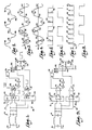
- a read channel circuit constructed and arranged in accordance with the present invention includes input lines 10 and 12 which receive the signal generated by a conventional inductive read head of the type commonly used in the reading of stored data from a magnetic medium such as a disk or tape.
- the read head has a sensitive gap which senses each flux transition in the magnetic recording track on the medium. Each flux transition which passes the sensitive gap results in the generation of a small voltage pulse, and it is this pulsed signal which is applied to the input lines 10 and 12.
- the read channel circuit includes a conventional filter which is generally designated by numeral 14 and which functions to filter high frequency noise from the signal. After passing through the filter 14, the filtered signal is applied to a pair of differentiator circuits 16 and 18.
- Differentiator 16 is a high resolution differentiator which includes a conventional differential amplifier 20 and an RC circuit formed by a resistor 22 and a capacitor 24. The components of the high resolution differentiator circuit are adjusted to accurately differentiate the filtered signal which is input to the differential amplifier 20.
- the other differentiator circuit 18 is a low resolution circuit which includes a differential amplifier 26 in combination with a resistor 28 and a capacitor 30.
- the resistance of the resistor 28 and the capacitance of capacitor 30 are selected such that the differentiation function performed by the differentiator circuit 18 is imperfect. As will be explained more fully, this imperfection provides a margin against spurious zero crossings in the differentiated signal in order to eliminate spurious peaks.
- Comparator 32 which functions as a zero crossing detector.
- Comparator 32 is preferably a high speed comparator, and its output lines are connected with the J and K inputs to a conventional JK flip flop 34. The data inputs to the flip flop 34 are thus provided by comparator 32.
- the output signal from the high resolution differentiator circuit 16 is similarly applied to a high speed comparator 36 which functions as a zero crossing detector.
- One output line from comparator 36 is applied as one input to an exclusive OR gate 38, while the other comparator output is applied to a pair of inverters 40 and 42 and then to the second input of gate 38.
- the output signal from gate 38 is applied to a delay circuit 44 which functions to delay the signal applied to it by a preselected time which, in the preferred embodiment, is approximately half of the minimum distance between flux-transitions.
- the output from the delay circuit is applied to the clock terminal 46 of the JK flip flop 34.
- the Q output line of flip flop 34 is indicated by numeral 47.
- each peak 48 (positive or negative) represents a flux transition in the magnetic recording track which is being read by the read head.
- the differentiation that is carried out by the high-resolution differentiator circuit 16 generates the saddle-shaped wave-form illustrated in Fig. 3. Since each peak 48 in the Fig. 2 wave form has a slope of zero, the differentiated signal shown in Fig. 3 crosses a value of zero at locations 50 which correspond to the peaks in the undifferentiated signal.
- Each saddle shape in the differentiated signal includes a "notch" 54 which corresponds to a "shoulder" 56 in the undifferentiated signal of Fig. 2. Since each shoulder 56 has a slope near zero, there is only a small gap 58 between each of the notches 54 and the value of zero. When noise and other signal distortions are present, the notches 54 can closely approach and even cross the value of zero in some instances, and this can cause a false zero crossing which can be detected as a spurious peak corresponding to a flux transition when in fact no flux transition is present.
- the differentiated signal produced by the low resolution differentiator circuit 18 is the saddle shaped circuit shown in F ig. 4. Zero crossings in the Fig. 4 wave form are present at the areas 60 which correspond to the peaks 48 in the undifferentiated signal. Again, each saddle shaped wave in the Fig. 4 signal has a notch 62. However, because of the imperfect manner in which the signal is differentiated by the low resolution differentiator circuit 18, each notch 62 is displaced from a value of zero by a gap 64 which is considerably greater than each of the gaps 58. The imperfection in the differentiation creates more of a margin against the detection of a false zero crossing because the slope of each shoulder 56 is reproduced as being farther away from zero than it actually is. In this manner, the relatively large gaps 64 provide a significant margin against the detection of false zero crossings in the low resolution Fig. 4 signal.
- Fig. 5 depicts a square wave signal which is generated by comparator 36.
- each side of each square wave is generated by the detection of one of the zero crossings 50 in the differentiated signal of Fig.
- Spurious pulses are identified by numeral 66 in F ig. 5, and the spurious pulses 66 are generated in those instances where each notch 54 in the differentiated signal closely approaches (or crosses) a value of zero such that the gap 58 essentially disappears and the notch is detected as being a zero crossing.
- the spurious pulses 66 thus represent false peaks in the waveform generated by the read head.
- Fig. 6 depicts a square wave signal which is produced on the output side of comparator 32.
- Each side of each wave in the Fig. 6 signal is formed by the detection of a zero crossing 60 in the differentiated signal of Fig. 4. It is noted that the gaps 64 are great enough that none of the notches 62 is interpreted as a false zero crossing, and there are thus no spurious pulses in the Fig. 6 waveform.
- Fig. 7 After the output signal from comparator 36 has been processed by the exclusive OR gate 38 and the delay circuit 44, it assumes the form shown in Fig. 7.
- Gate 38 converts each signal transition to a pulse 68.
- Each pulse 68 shown in the Fig. 7 signal represents a flux transition in the read head signal, and the gap 70 represents the time delay created by the delay circuit 44. The delay is for the purpose of assuring that the data signals are applied to the J and K inputs of flip flop 34 at the time of application of the clock signal at terminal 46.
- the signal of Fig. 7 includes spurious pulses 72 which are present due to the presence of the spurious pulses 66 in the signal shown in Fig. 5.
- the low resolution signal shown in Fig. 6 is applied to the J and K data inputs of flip flop 34, while the high resolution signal of Fig. 7 is applied to the clock terminal 46 of the flip-flop. Because the low resolution data signal to flip-flop 34 is devoid of spurious pulses, the spurious pulses 72 that are present in the high resolution path (clock input) do not cause the flip-flop to change state, and the spurious pulses are eliminated in the output of the flip-flop 34. By combining the low and high resolution signals in the flip-flop, the output applied to the Q output line of the flip-flop takes the form of the square wave signal shown in Fig. 8, and the spurious pulses are eliminated by the flip-flop.
- the read channel circuit takes full advantage of the accurate timing provided by the high resolution differentiator circuit 16 and the good discrimination against false peaks that is provided by the low resolution differentiator circuit 18.
- the circuit is relatively insensitive to amplitude of the input signal and requires only the single filter 14.
- the added differentiator circuit that is required is formed by conventional off the shelf items that do not add appreciably either to the cost or the space requirements of the circuit. Additionally, there is only minimal phase mismatching in the outputs from the two differentiator circuits, so the phase responses of the differentiators do not create significant problems due to mismatching.
- F ig. 9 illustrates an alternative read channel circuit which is arranged for the most part identically to the circuit shown in Fig. 1.
- the Fig. 9 circuit uses a D type flip-flop 134 having its data input D tied to the output from the comparator 32 for the low resolution path. The output from the delay circuit 44 is applied to the clock input 46.
- the D type flip-flop 134 uses the high and low resolution signals to eliminate the effects of spurious pulses that may be generated by the detection of false peaks in the read head signal. It is important to recognize that either the JK flip-flop 34 or the D type flip-flop 134 can be used in the circuit, as can other components which provide the same function.
Landscapes
- Engineering & Computer Science (AREA)
- Signal Processing (AREA)
- Digital Magnetic Recording (AREA)
- Dc Digital Transmission (AREA)
Applications Claiming Priority (2)
| Application Number | Priority Date | Filing Date | Title |
|---|---|---|---|
| US893973 | 1986-08-07 | ||
| US06/893,973 US4849834A (en) | 1986-08-07 | 1986-08-07 | Read channel architecture for processing read head signals |
Publications (2)
| Publication Number | Publication Date |
|---|---|
| EP0258671A2 true EP0258671A2 (fr) | 1988-03-09 |
| EP0258671A3 EP0258671A3 (fr) | 1988-10-19 |
Family
ID=25402423
Family Applications (1)
| Application Number | Title | Priority Date | Filing Date |
|---|---|---|---|
| EP87111371A Withdrawn EP0258671A3 (fr) | 1986-08-07 | 1987-08-06 | Architecture d'un canal de lecture pour le traitement des signaux d'une tête de lecture |
Country Status (4)
| Country | Link |
|---|---|
| US (1) | US4849834A (fr) |
| EP (1) | EP0258671A3 (fr) |
| JP (1) | JPS6344303A (fr) |
| AU (1) | AU7446587A (fr) |
Cited By (1)
| Publication number | Priority date | Publication date | Assignee | Title |
|---|---|---|---|---|
| EP0333592A3 (en) * | 1988-03-16 | 1990-12-19 | Fujitsu Limited | Data reproducing circuit for memory system and having equalizer generating two different equalizing signals used for data reproduction |
Families Citing this family (4)
| Publication number | Priority date | Publication date | Assignee | Title |
|---|---|---|---|---|
| US5455816A (en) * | 1992-05-18 | 1995-10-03 | At&T Global Information Solutions Company | MOS amplifier with gain control |
| US5424881A (en) * | 1993-02-01 | 1995-06-13 | Cirrus Logic, Inc. | Synchronous read channel |
| US5396240A (en) * | 1993-09-01 | 1995-03-07 | Maxtor Corporation | Missing pulse generator for gray code decoding |
| US20100061023A1 (en) * | 2008-09-11 | 2010-03-11 | Tdk Corporation | Magnetic head device and magnetic disk drive apparatus with the magnetic head device |
Family Cites Families (3)
| Publication number | Priority date | Publication date | Assignee | Title |
|---|---|---|---|---|
| US4495529A (en) * | 1982-05-07 | 1985-01-22 | Digital Equipment Corporation | Qualifier circuit |
| US4517610A (en) * | 1982-12-09 | 1985-05-14 | Magnetic Peripherals Inc. | Multichannel signal recovery circuit |
| JPS60243872A (ja) * | 1984-05-17 | 1985-12-03 | Seiko Epson Corp | 磁気再生装置 |
-
1986
- 1986-08-07 US US06/893,973 patent/US4849834A/en not_active Expired - Fee Related
-
1987
- 1987-06-18 AU AU74465/87A patent/AU7446587A/en not_active Abandoned
- 1987-08-03 JP JP62192765A patent/JPS6344303A/ja active Pending
- 1987-08-06 EP EP87111371A patent/EP0258671A3/fr not_active Withdrawn
Cited By (2)
| Publication number | Priority date | Publication date | Assignee | Title |
|---|---|---|---|---|
| EP0333592A3 (en) * | 1988-03-16 | 1990-12-19 | Fujitsu Limited | Data reproducing circuit for memory system and having equalizer generating two different equalizing signals used for data reproduction |
| US5068753A (en) * | 1988-03-16 | 1991-11-26 | Fujitsu Limited | Data reproducing circuit for memory system having an equalizer generating two different equalizing signals used for data reproduction |
Also Published As
| Publication number | Publication date |
|---|---|
| AU7446587A (en) | 1988-02-11 |
| JPS6344303A (ja) | 1988-02-25 |
| US4849834A (en) | 1989-07-18 |
| EP0258671A3 (fr) | 1988-10-19 |
Similar Documents
| Publication | Publication Date | Title |
|---|---|---|
| US5311178A (en) | Method for processing sample values in an RLL channel | |
| US4081756A (en) | Dual channel signal detector circuit | |
| US4697098A (en) | Composite gate generator circuit for detecting valid data signals | |
| KR910005904B1 (ko) | 진폭 및 시간검정을 사용하는 펄스검출 회로 및 방법 | |
| US4346411A (en) | Amplitude sensitive three-level detector for derivative read back channel of magnetic storage device | |
| US4965873A (en) | Pilot enhanced/amplitude equalized impulse magnetic | |
| JPH09213007A (ja) | データ再生装置 | |
| US4849834A (en) | Read channel architecture for processing read head signals | |
| US5105316A (en) | Qualification for pulse detecting in a magnetic media data storage system | |
| US4341964A (en) | Precision time duration detector | |
| US4724496A (en) | Peak detector for magnetically recorded binary signal | |
| US4016599A (en) | Anti-shouldering read circuit for magnetic disk memory | |
| KR940000974B1 (ko) | 디지탈 신호 처리회로 | |
| US5420726A (en) | Channel qualifier for a hard disk drive which differentiates a raw data signal before peak detection and qualification of the signal | |
| US4686586A (en) | Read back circuit for recovering data from magnetic storage medium | |
| EP0091304B1 (fr) | Méthode et système pour le rétablissement de la polarité à courant continu dans un enregistrement magnétique | |
| US4012785A (en) | Magnetic recording playback circuit | |
| US4544963A (en) | Read signal detection in ternary 3PM magnetic recording | |
| JPS61214278A (ja) | 情報再生方式 | |
| US3581215A (en) | Variable frequency delay line differentiator | |
| JP2763454B2 (ja) | データ検出装置 | |
| US4813059A (en) | Readback recovery of run length limited codes | |
| US3778792A (en) | Blanking circuit for high resolution data recovery systems | |
| JP3643589B2 (ja) | 3進信号から2進信号を生成する回路 | |
| Graham | Data detection methods vs head resolution in digital magnetic recording |
Legal Events
| Date | Code | Title | Description |
|---|---|---|---|
| PUAI | Public reference made under article 153(3) epc to a published international application that has entered the european phase |
Free format text: ORIGINAL CODE: 0009012 |
|
| AK | Designated contracting states |
Kind code of ref document: A2 Designated state(s): AT BE CH DE ES FR GB GR IT LI LU NL SE |
|
| PUAL | Search report despatched |
Free format text: ORIGINAL CODE: 0009013 |
|
| AK | Designated contracting states |
Kind code of ref document: A3 Designated state(s): AT BE CH DE ES FR GB GR IT LI LU NL SE |
|
| STAA | Information on the status of an ep patent application or granted ep patent |
Free format text: STATUS: THE APPLICATION IS DEEMED TO BE WITHDRAWN |
|
| 18D | Application deemed to be withdrawn |
Effective date: 19890420 |
|
| RIN1 | Information on inventor provided before grant (corrected) |
Inventor name: ALLEN, DAVID M |