EP0258848A2 - Flüssigkristallvorrichtung und Verfahren zu ihrer Herstellung mit Hilfe von Abstandshaltern, die durch Aufdrucken geformt werden - Google Patents
Flüssigkristallvorrichtung und Verfahren zu ihrer Herstellung mit Hilfe von Abstandshaltern, die durch Aufdrucken geformt werden Download PDFInfo
- Publication number
- EP0258848A2 EP0258848A2 EP87112591A EP87112591A EP0258848A2 EP 0258848 A2 EP0258848 A2 EP 0258848A2 EP 87112591 A EP87112591 A EP 87112591A EP 87112591 A EP87112591 A EP 87112591A EP 0258848 A2 EP0258848 A2 EP 0258848A2
- Authority
- EP
- European Patent Office
- Prior art keywords
- liquid crystal
- substrates
- pair
- printing
- pillar
- Prior art date
- Legal status (The legal status is an assumption and is not a legal conclusion. Google has not performed a legal analysis and makes no representation as to the accuracy of the status listed.)
- Granted
Links
Images

Classifications
-
- G—PHYSICS
- G02—OPTICS
- G02F—OPTICAL DEVICES OR ARRANGEMENTS FOR THE CONTROL OF LIGHT BY MODIFICATION OF THE OPTICAL PROPERTIES OF THE MEDIA OF THE ELEMENTS INVOLVED THEREIN; NON-LINEAR OPTICS; FREQUENCY-CHANGING OF LIGHT; OPTICAL LOGIC ELEMENTS; OPTICAL ANALOGUE/DIGITAL CONVERTERS
- G02F1/00—Devices or arrangements for the control of the intensity, colour, phase, polarisation or direction of light arriving from an independent light source, e.g. switching, gating or modulating; Non-linear optics
- G02F1/01—Devices or arrangements for the control of the intensity, colour, phase, polarisation or direction of light arriving from an independent light source, e.g. switching, gating or modulating; Non-linear optics for the control of the intensity, phase, polarisation or colour
- G02F1/13—Devices or arrangements for the control of the intensity, colour, phase, polarisation or direction of light arriving from an independent light source, e.g. switching, gating or modulating; Non-linear optics for the control of the intensity, phase, polarisation or colour based on liquid crystals, e.g. single liquid crystal display cells
- G02F1/133—Constructional arrangements; Operation of liquid crystal cells; Circuit arrangements
- G02F1/1333—Constructional arrangements; Manufacturing methods
- G02F1/1339—Gaskets; Spacers; Sealing of cells
- G02F1/13394—Gaskets; Spacers; Sealing of cells spacers regularly patterned on the cell subtrate, e.g. walls, pillars
-
- G—PHYSICS
- G02—OPTICS
- G02F—OPTICAL DEVICES OR ARRANGEMENTS FOR THE CONTROL OF LIGHT BY MODIFICATION OF THE OPTICAL PROPERTIES OF THE MEDIA OF THE ELEMENTS INVOLVED THEREIN; NON-LINEAR OPTICS; FREQUENCY-CHANGING OF LIGHT; OPTICAL LOGIC ELEMENTS; OPTICAL ANALOGUE/DIGITAL CONVERTERS
- G02F1/00—Devices or arrangements for the control of the intensity, colour, phase, polarisation or direction of light arriving from an independent light source, e.g. switching, gating or modulating; Non-linear optics
- G02F1/01—Devices or arrangements for the control of the intensity, colour, phase, polarisation or direction of light arriving from an independent light source, e.g. switching, gating or modulating; Non-linear optics for the control of the intensity, phase, polarisation or colour
- G02F1/13—Devices or arrangements for the control of the intensity, colour, phase, polarisation or direction of light arriving from an independent light source, e.g. switching, gating or modulating; Non-linear optics for the control of the intensity, phase, polarisation or colour based on liquid crystals, e.g. single liquid crystal display cells
- G02F1/133—Constructional arrangements; Operation of liquid crystal cells; Circuit arrangements
- G02F1/1333—Constructional arrangements; Manufacturing methods
- G02F1/1339—Gaskets; Spacers; Sealing of cells
- G02F1/13392—Gaskets; Spacers; Sealing of cells spacers dispersed on the cell substrate, e.g. spherical particles, microfibres
-
- Y—GENERAL TAGGING OF NEW TECHNOLOGICAL DEVELOPMENTS; GENERAL TAGGING OF CROSS-SECTIONAL TECHNOLOGIES SPANNING OVER SEVERAL SECTIONS OF THE IPC; TECHNICAL SUBJECTS COVERED BY FORMER USPC CROSS-REFERENCE ART COLLECTIONS [XRACs] AND DIGESTS
- Y10—TECHNICAL SUBJECTS COVERED BY FORMER USPC
- Y10S—TECHNICAL SUBJECTS COVERED BY FORMER USPC CROSS-REFERENCE ART COLLECTIONS [XRACs] AND DIGESTS
- Y10S359/00—Optical: systems and elements
- Y10S359/90—Methods
Definitions
- the present invention relates to a liquid crystal device and a method for manufacturing same.
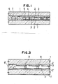
- the device such as a liquid crystal display, comprises a pair of substrates 1 and 1 ⁇ joined to each other with a suitable distance inbetween, a liquid crystal layer 5 disposed between the pair of substrates 1 and 1 ⁇ , opposed electrodes 2 and 2 ⁇ formed on the opposed inside surfaces of the substrates 1 and 1 ⁇ in the form of a matrix, and oriented coating 3 and 3 ⁇ on the opposed insides contiguous to the liquid crystal layer 5.
- a voltage to the electrodes 2 and 2 ⁇
- the optical characteristics of the liquid crystal 5 is changed under the electric field induced by the applied voltage.
- the device can be controlled by applying an voltage selectively to each pixel of the matrix to display an image or picture or storing information in terms of encoded signals.
- the distance between the opposed substrates 1 and 1 ⁇ is about 10 microns, while the device with the distance of 5 microns are now being developed. Although devices having twisted nematic liquid crystal can be constructed with the distances of this scale, the distance is demanded to be decreased to less than 3 microns, generally 2 ⁇ 0.5 microns, when making use of a ferroelectric liquid crystal for the device in place of a nematic liquid crystal.
- the distance has been kept by disposing spacers 7 and 4 between the paid of substrates 1 and 1 ⁇ .
- two kind of spacers are illustrated; one being mixed with a sealing member 6 and the other being disposed between the opposed electrodes 2 and 2 ⁇ .
- the spacers 4 are a plurality of spherical particles made of an organic resin such as Micro Pearl SP-210 having the average diameter of 10.0 ⁇ 0.5 microns made of a bridged polymer of divinyl benzene.
- the spacers of Micro Pearl SP-210 are perfect spheres.
- the spacers 4 prevent the substrates 1 and 1 ⁇ from contact due to unevenness of the substrates or due to external stress.
- the spacers 4 and the electrodes 2 and 2 ⁇ are in point contact so that the electrodes 2 and 2 ⁇ are subjected to concentrated stress.
- the concentrated stress may destroy the active devices or disconnect electrode curcuits, and therefore make the liquid device defective.
- it is very difficult to obtain a constant distance between the substrates because the spacers, when distributed between the substrates, tend to aggregate to local positions on the substrates and because the diameters of spacers are not constant. Even if uniform distribution of the spacers be obtained between the substrates, the distribution is disturbed during filling process of liquid crystal.
- the liquid crystal is charged into the distance by virtue of capillary action from an opening provided on a portion of sealed-off perimeter of the substrates in the manner that the entrance is dipped in an amount of liquid crystal in a vacuum condition and then the pressure is increased so that the liquid crystal is caused to enter the device through the opening by the differential pressure. So, the stream of the liquid crystal tends to move the distributed spacers. Because of this unevenness of the distance, color shade appears on a display with a ferroelectric liquid crystal which utilizes birefringence. The defect can appear only due to external stress, such as push with a finger.
- the liquid crystal device comprises a pair of transparent substrates 1 and 1 ⁇ which are mated with 3 microns, e.g., 2.2 ⁇ 0.5 microns, in distance, a plurality of first electrode strips 2 and a plurality of second electrode strips 2 ⁇ both made of conductive transparent oxide such as indium tin oxide SnO2 or the like and elongated in orthogonal directions to constitute a matrix, a plularity of pillars 9 as spacers and a sealing member 9 ⁇ , both being made of an adhesive, e.g.
- an epoxy resin such as "UV-307” distributed from Grace Japan Ltd.
- a liquid crystal layer disposed between the substrates 1 and 1 ⁇ .
- the inside surfaces of the substrates 1 and 1 ⁇ are coated with 500 ⁇ thick oriented thin films 3 made of a polyimide over the first and second electrode strips 2 and 2 ⁇ respectively.
- the oriented films are given rubbing treatment.
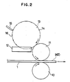
- the printing press machine comprises a container 12 filled with an epoxy resin adhesive, a cylinder 13 whose surface is scratched in accordance with a prescribed pattern 14, a squeegee 15, a printing roll 11 engaged with the cylinder 13 and an accompanying roll 10 provided just below the printing roll 11 with a suitable internal therebetween.
- the adhesive in the container 12 is diluted with a thinner to 200 centipoises - 100 poises.
- a substrate 1 having been provided with a first electrode strips and an oriented film is placed between the printing roll 10 and the accompanying roll 11 and caused to move to the right side as the two rolls are turning.
- the surface of the cylinder 13 passes through the adhesive in the container 12 and receive it thereon.
- the adhesive on the surface of the cylinder 13 is pushed off by the squeegee 15, remaining the portion in the scratched pattern 14.
- the printing roll 11 receives the adhesive in the pattern 14 as engaging with the cylinder 13.
- the surface of the substrate 1 is printed with the adhesive in accordance with the pattern 14.
- the printed adhesive becomes the pillars 9 and the sealing member 9 ⁇ shown in Fig.2.
- the height of the pillars 9 is about 20 microns, when printed on the substrate, which can be controlled depending on the diameter of pillar.
- the sealing member 9 ⁇ is formed with an opening for charging a liquid crystal into the liquid crystal device therethrough.
- the pillars 9 on the electrode strips 2 have a cross section of 20 microns x 20 microns respectively with intervals of 400 microns inbetween.
- the substrate provided with the sealing resin layer 9 ⁇ and the pillars 9 is mated in a vacuum with an opposed substrate 1 ⁇ which is provided with a plurality of second transparent electrode strips elengated in the direction perpendicular to the first electrode strips 2 on the substrate 1 as shown in Fig.2.
- the mated substates 1 and 1 ⁇ are fixed by baking at 150°C for an hour under a pressure applied from both external sides of the mated substrated.
- the thickness is reduced to less than 3 microns, e.g., 2 ⁇ 0.5 microns, which is suitable for a ferroelectric liquid crystal device.
- the distance between the substrates is kept constant even if the substrate is slightly warped because the pillars having a same height urge the substrates to compensate each other.
- a ferroelectric liquid crystal is disposed by an existing method.
- the distance between substrates of 200 mm x 300 mm joined in accordance with the present invention was measured.
- Nine measuring points were taken on the diagonal line of the substrates with an interval of 40 mm.
- 10 designates the results in Fig.3.
- 11 designates the corresponding distances of a device produced by a prior art process with spacers made of almina having 2.0 ⁇ 0.3 microns in diameter which are distributed with methyl alchol.
- the distance in accordance with the invention is largely constant while the distance in accordance with the prior art is substantially scattered, and particularly is wide at the center position.
- the distance is substantially not changed even when pushed with a finger. The fluctuation was only ⁇ 0.5 micron.
- the invention is applied to a liquid crystal panel of 20 cm x 30 cm formed with an active matrix structure having 400 x 1920 pixels, the distance between a pair of substrates was also kept constant.
- finely finishing of the surface of a substrate can be dispensed with by means of provision of pillars as explained above.
- the cost of such finishing is higher than the price of a substrate for liquid crystal device, so that the price can be lowered by a factor of 2 to 5.
- sealing process and spacer distributing process are implemented simultaneously.
- spacers are prepared with an interval of 400 microns, corresponding to the interval between adjacent pixels, so that the device constracted with the spacers has resistance against external impact.
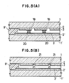
- Figs5(A) and 5(B) are cross sections showing second and third embodiments of the invention.
- pillars are formed with spheres 19 and adhesive 20 applied to the spheres for preventing the position of the spheres on the substrates 1 and 1 ⁇ .
- the adhesive 20 can be dispensed with.
- the spheres 19 are pressed between the substrates 1 and 1 ⁇ at a high temperature, and melt at their contact portions with the substrates. Namely, the spheres 19 and the substrates are fused by heating.
- Fig.5(B) are prepered merely to show the pillars 14 can be provided between adjacent pillars.
- the present invention should not limited to these particular embodiments but only limited to the appended cliams. Many modifications and variations may cause to those skilled in the art without departing the spirit of the invention.
- the pillars 9 can be provided in the form of stripes or blocks.
- the pillars and the sealing members can be formed by screen printing.
Landscapes
- Physics & Mathematics (AREA)
- Nonlinear Science (AREA)
- Mathematical Physics (AREA)
- Chemical & Material Sciences (AREA)
- Crystallography & Structural Chemistry (AREA)
- General Physics & Mathematics (AREA)
- Optics & Photonics (AREA)
- Liquid Crystal (AREA)
Applications Claiming Priority (2)
| Application Number | Priority Date | Filing Date | Title |
|---|---|---|---|
| JP61208617A JPS6363020A (ja) | 1986-09-04 | 1986-09-04 | 液晶電気光学装置作製方法 |
| JP208617/86 | 1986-09-04 |
Publications (3)
| Publication Number | Publication Date |
|---|---|
| EP0258848A2 true EP0258848A2 (de) | 1988-03-09 |
| EP0258848A3 EP0258848A3 (en) | 1988-09-21 |
| EP0258848B1 EP0258848B1 (de) | 1993-03-10 |
Family
ID=16559188
Family Applications (1)
| Application Number | Title | Priority Date | Filing Date |
|---|---|---|---|
| EP87112591A Expired - Lifetime EP0258848B1 (de) | 1986-09-04 | 1987-08-28 | Flüssigkristallvorrichtung und Verfahren zu ihrer Herstellung mit Hilfe von Abstandshaltern, die durch Aufdrucken geformt werden |
Country Status (4)
| Country | Link |
|---|---|
| US (1) | US4924243A (de) |
| EP (1) | EP0258848B1 (de) |
| JP (1) | JPS6363020A (de) |
| DE (1) | DE3784597T2 (de) |
Cited By (5)
| Publication number | Priority date | Publication date | Assignee | Title |
|---|---|---|---|---|
| US5005951A (en) * | 1987-06-10 | 1991-04-09 | U.S. Philips Corporation | Liquid crystal display device |
| US5054890A (en) * | 1988-06-23 | 1991-10-08 | Canon Kabushiki Kaisha | Liquid crystal device |
| US5089905A (en) * | 1987-06-02 | 1992-02-18 | Toppan Printing Co., Ltd. | Color liquid crystal display system with spacer-adhesive and separate rigid spacers across display surface |
| EP0288304B1 (de) * | 1987-04-22 | 1993-03-17 | Sharp Kabushiki Kaisha | Flüssigkristall-Anzeigevorrichtung |
| CN103529600A (zh) * | 2013-10-23 | 2014-01-22 | 京东方科技集团股份有限公司 | 一种隔垫物及其制作方法、显示器 |
Families Citing this family (41)
| Publication number | Priority date | Publication date | Assignee | Title |
|---|---|---|---|---|
| US5365357A (en) * | 1988-04-21 | 1994-11-15 | Asahi Glass Company Ltd. | Color liquid crystal display having color filters and light blocking layers in the periphery |
| US5276541A (en) * | 1989-05-19 | 1994-01-04 | International Business Machines Corporation | Method for forming a liquid crystal display with a sealing member |
| JP2873256B2 (ja) * | 1991-02-01 | 1999-03-24 | シャープ 株式会社 | 液晶表示装置 |
| US5177629A (en) * | 1991-06-13 | 1993-01-05 | Proxima Corporation | Liquid crystal display with an optical fluid layer |
| US5739882A (en) * | 1991-11-18 | 1998-04-14 | Semiconductor Energy Laboratory Co., Ltd. | LCD polymerized column spacer formed on a modified substrate, from an acrylic resin, on a surface having hydrophilic and hydrophobic portions, or at regular spacings |
| DE69417124T2 (de) * | 1993-01-26 | 1999-11-18 | Hughes Electronics Corp., El Segundo | Flüssigkristallzelle mit distanzelementen und verfahren zu ihrer herstellung |
| US5546208A (en) * | 1993-02-19 | 1996-08-13 | Semiconductor Energy Laboratory Co., Ltd. | Electrooptical device involving a mixture of liquid crystal, photo curable resins and reaction initiating material for forming resinous columns |
| JP3210126B2 (ja) * | 1993-03-15 | 2001-09-17 | 株式会社東芝 | 液晶表示装置の製造方法 |
| US5539545A (en) * | 1993-05-18 | 1996-07-23 | Semiconductor Energy Laboratory Co., Ltd. | Method of making LCD in which resin columns are cured and the liquid crystal is reoriented |
| DE19649761C2 (de) * | 1996-11-30 | 2003-04-03 | Univ Stuttgart | Verfahren zur Herstellung von Flüssigkristall-Displays auf Kunststoff-Folien unter Verwendung von bistabilen Flüssigkristallen |
| US6326067B1 (en) | 1999-05-03 | 2001-12-04 | Guardian Industries Corporation | Vacuum IG pillar with DLC coating |
| US6336984B1 (en) | 1999-09-24 | 2002-01-08 | Guardian Industries Corporation | Vacuum IG window unit with peripheral seal at least partially diffused at temper |
| US6291036B1 (en) | 1999-05-03 | 2001-09-18 | Guardian Industries Corporation | Vacuum IG window unit with spacers in seal |
| US6399169B1 (en) | 1999-07-07 | 2002-06-04 | Guardian Industries Corp. | Vacuum IG window unit with dual peripheral seal |
| US6365242B1 (en) | 1999-07-07 | 2002-04-02 | Guardian Industries Corp. | Peripheral seal for vacuum IG window unit |
| US6420002B1 (en) | 1999-08-18 | 2002-07-16 | Guardian Industries Corp. | Vacuum IG unit with spacer/pillar getter |
| US6946171B1 (en) | 1999-09-22 | 2005-09-20 | Guardian Industries Corp. | Vacuum IG pillar with lubricating and/or reflective coating |
| US6558494B1 (en) | 1999-09-24 | 2003-05-06 | Guardian Industries Corp. | Vacuum IG window unit with edge seal at least partially diffused at temper and completed via microwave curing, and corresponding method of making the same |
| US6444281B1 (en) | 1999-10-13 | 2002-09-03 | Guardian Industries Corp. | Vacuum IG window unit with spacers between first and second edge seals |
| US6383580B1 (en) | 1999-11-12 | 2002-05-07 | Guardian Industries Corp. | Vacuum IG window unit with edge mounted pump-out tube |
| US6436492B1 (en) | 1999-11-16 | 2002-08-20 | Guardian Industries Corp. | Vacuum IG window unit with fiber spacers |
| US6503583B2 (en) | 1999-11-16 | 2003-01-07 | Guardian Industries Corp. | Vacuum IG window unit with fiber inclusive edge seal |
| US6352749B1 (en) | 1999-12-10 | 2002-03-05 | Guardian Industries Corp. | Vacuum IG unit with transparent spacers |
| US6497931B1 (en) | 2000-01-11 | 2002-12-24 | Guardian Industries Corp. | Vacuum IG unit with colored spacers |
| US6541083B1 (en) | 2000-01-11 | 2003-04-01 | Guardian Industries Corp. | Vacuum IG unit with alkali silicate edge seal and/or spacers |
| US6372312B1 (en) | 2000-02-17 | 2002-04-16 | Guardian Industries Corp. | Vacuum IG unit with micro-sized spacers |
| US6506272B1 (en) | 2000-04-04 | 2003-01-14 | Guardian Industries Corp. | Vacuum IG unit with seal for pump-out aperture |
| US6701749B2 (en) | 2000-09-27 | 2004-03-09 | Guardian Industries Corp. | Vacuum IG window unit with edge seal at least partially diffused at temper and completed via microwave curing, and corresponding method of making the same |
| KR100416761B1 (ko) * | 2001-06-12 | 2004-01-31 | 삼성에스디아이 주식회사 | 평판 표시 소자의 스페이서 형성방법 |
| US20030232126A1 (en) * | 2002-06-14 | 2003-12-18 | Yang Michael W. | Method for dispersing spacer on the substrate of a liquid crystal display element and apparatus for dispersion therewith |
| KR101160833B1 (ko) * | 2005-07-11 | 2012-06-28 | 삼성전자주식회사 | 액정 표시 장치의 제조 장치 |
| KR20070087330A (ko) * | 2006-02-23 | 2007-08-28 | 삼성전자주식회사 | 액정 표시 장치의 제조 장치 및 제조 방법 |
| US20070203267A1 (en) * | 2006-02-28 | 2007-08-30 | 3M Innovative Properties Company | Optical display with fluted optical plate |
| US7766531B2 (en) * | 2006-03-29 | 2010-08-03 | 3M Innovative Properties Company | Edge-lit optical display with fluted optical plate |
| KR101316632B1 (ko) * | 2006-08-16 | 2013-10-15 | 삼성디스플레이 주식회사 | 인쇄장치 및 이를 이용한 스페이서의 인쇄방법 |
| JP4623043B2 (ja) * | 2007-04-11 | 2011-02-02 | 日立化成工業株式会社 | 液晶表示装置 |
| JP2009134274A (ja) * | 2007-10-30 | 2009-06-18 | Semiconductor Energy Lab Co Ltd | 液晶表示装置の作製方法 |
| US10280680B2 (en) | 2013-12-31 | 2019-05-07 | Guardian Glass, LLC | Vacuum insulating glass (VIG) unit with pump-out port sealed using metal solder seal, and/or method of making the same |
| US9784027B2 (en) | 2013-12-31 | 2017-10-10 | Guardian Glass, LLC | Vacuum insulating glass (VIG) unit with metallic peripheral edge seal and/or methods of making the same |
| US10012019B2 (en) | 2013-12-31 | 2018-07-03 | Guardian Glass, LLC | Vacuum insulating glass (VIG) unit with metallic peripheral edge seal and/or methods of making the same |
| US10145005B2 (en) | 2015-08-19 | 2018-12-04 | Guardian Glass, LLC | Techniques for low temperature direct graphene growth on glass |
Family Cites Families (13)
| Publication number | Priority date | Publication date | Assignee | Title |
|---|---|---|---|---|
| US3684614A (en) * | 1969-08-11 | 1972-08-15 | Jerome H Lemelson | Process for the manufacture of optical display devices |
| US3742600A (en) * | 1971-07-26 | 1973-07-03 | Research Frontiers Inc | Method for maintaining the separation of plates |
| US4187340A (en) * | 1973-05-14 | 1980-02-05 | Asahi Glass Company, Ltd. | Method of forming patterned transparent electro-conductive film on the substrate of liquid crystal display |
| DE2805970C3 (de) * | 1978-02-13 | 1980-09-25 | Siemens Ag, 1000 Berlin Und 8000 Muenchen | Flüssigkristall-Anzeigevorrichtung |
| JPS583212B2 (ja) * | 1978-06-02 | 1983-01-20 | 株式会社日立製作所 | 液晶表示素子の製造方法 |
| US4367924A (en) * | 1980-01-08 | 1983-01-11 | Clark Noel A | Chiral smectic C or H liquid crystal electro-optical device |
| JPS6027966A (ja) * | 1983-07-27 | 1985-02-13 | Hitachi Ltd | データ処理装置 |
| JPS6034848A (ja) * | 1983-08-06 | 1985-02-22 | Isowa Ind Co | フイルムベ−スへの印版貼付け方法およびこれを実施するための装置 |
| JPS60188925A (ja) * | 1984-03-09 | 1985-09-26 | Canon Inc | 光学変調素子の製造法 |
| JPS61147232A (ja) * | 1984-12-20 | 1986-07-04 | Canon Inc | 液晶素子 |
| JPS61173222A (ja) * | 1985-01-28 | 1986-08-04 | Semiconductor Energy Lab Co Ltd | 液晶表示装置 |
| EP0213184A1 (de) * | 1985-03-05 | 1987-03-11 | AT&T Corp. | Elektro-optische anzeigevorrichtung von gleichmässiger niedriger dicke |
| US4643532A (en) * | 1985-06-24 | 1987-02-17 | At&T Bell Laboratories | Field-assisted bonding method and articles produced thereby |
-
1986
- 1986-09-04 JP JP61208617A patent/JPS6363020A/ja active Pending
-
1987
- 1987-08-28 EP EP87112591A patent/EP0258848B1/de not_active Expired - Lifetime
- 1987-08-28 DE DE8787112591T patent/DE3784597T2/de not_active Expired - Fee Related
-
1988
- 1988-05-23 US US07/197,434 patent/US4924243A/en not_active Expired - Lifetime
Cited By (6)
| Publication number | Priority date | Publication date | Assignee | Title |
|---|---|---|---|---|
| EP0288304B1 (de) * | 1987-04-22 | 1993-03-17 | Sharp Kabushiki Kaisha | Flüssigkristall-Anzeigevorrichtung |
| US5089905A (en) * | 1987-06-02 | 1992-02-18 | Toppan Printing Co., Ltd. | Color liquid crystal display system with spacer-adhesive and separate rigid spacers across display surface |
| US5005951A (en) * | 1987-06-10 | 1991-04-09 | U.S. Philips Corporation | Liquid crystal display device |
| US5054890A (en) * | 1988-06-23 | 1991-10-08 | Canon Kabushiki Kaisha | Liquid crystal device |
| CN103529600A (zh) * | 2013-10-23 | 2014-01-22 | 京东方科技集团股份有限公司 | 一种隔垫物及其制作方法、显示器 |
| CN103529600B (zh) * | 2013-10-23 | 2016-01-06 | 京东方科技集团股份有限公司 | 一种隔垫物及其制作方法、显示器 |
Also Published As
| Publication number | Publication date |
|---|---|
| DE3784597T2 (de) | 1993-06-17 |
| JPS6363020A (ja) | 1988-03-19 |
| EP0258848A3 (en) | 1988-09-21 |
| US4924243A (en) | 1990-05-08 |
| EP0258848B1 (de) | 1993-03-10 |
| DE3784597D1 (de) | 1993-04-15 |
Similar Documents
| Publication | Publication Date | Title |
|---|---|---|
| EP0258848A2 (de) | Flüssigkristallvorrichtung und Verfahren zu ihrer Herstellung mit Hilfe von Abstandshaltern, die durch Aufdrucken geformt werden | |
| US4874461A (en) | Method for manufacturing liquid crystal device with spacers formed by photolithography | |
| US5963288A (en) | Liquid crystal device having sealant and spacers made from the same material | |
| US5379139A (en) | Liquid crystal device and method for manufacturing same with spacers formed by photolithography | |
| JP3122985B2 (ja) | 液晶表示素子及びその製造方法 | |
| CA2132751C (en) | Improved liquid crystal light valves using internal, fixed spacers and method of incorporating same | |
| US6018380A (en) | LCD having trench formed on the substrate(s) to stop sealing material flowing to display areas | |
| JPS63128315A (ja) | 液晶表示素子 | |
| US7796233B2 (en) | Liquid crystal display and manufacturing method thereof | |
| EP0788013B1 (de) | Elektrodensubstrat für Flüssigkristallvorrichtung und Verfahren zu seiner Herstellung | |
| US6873391B2 (en) | LCD panel and method for fabricating the same | |
| JPH0679122B2 (ja) | 電気光学装置 | |
| US5754263A (en) | Liquid crystal display apparatus with silicon or silicon-germanium thin films cover spaces between electrodes | |
| US5847793A (en) | Liquid crystal display apparatus and fabrication process thereof | |
| JPS61173221A (ja) | 液晶表示装置作成方法 | |
| US6881455B2 (en) | Liquid crystal display element | |
| JP2933790B2 (ja) | 液晶表示素子の製造方法 | |
| KR100502806B1 (ko) | 액정표시장치및그제조방법 | |
| JPH04256925A (ja) | 液晶表示装置におけるスペーサの形成方法 | |
| CN113985635A (zh) | 显示面板及其制造方法、显示装置 | |
| US20060187399A1 (en) | Method for forming spacer on substrate | |
| JPH10133205A (ja) | 液晶表示装置 | |
| JPH032832A (ja) | 液晶表示パネル | |
| JP2000214469A (ja) | 液晶表示素子 | |
| JPS6224229A (ja) | 液晶電気光学装置作製方法 |
Legal Events
| Date | Code | Title | Description |
|---|---|---|---|
| PUAI | Public reference made under article 153(3) epc to a published international application that has entered the european phase |
Free format text: ORIGINAL CODE: 0009012 |
|
| AK | Designated contracting states |
Kind code of ref document: A2 Designated state(s): DE FR GB |
|
| PUAL | Search report despatched |
Free format text: ORIGINAL CODE: 0009013 |
|
| AK | Designated contracting states |
Kind code of ref document: A3 Designated state(s): DE FR GB |
|
| 17P | Request for examination filed |
Effective date: 19890321 |
|
| 17Q | First examination report despatched |
Effective date: 19910405 |
|
| GRAA | (expected) grant |
Free format text: ORIGINAL CODE: 0009210 |
|
| AK | Designated contracting states |
Kind code of ref document: B1 Designated state(s): DE FR GB |
|
| ET | Fr: translation filed | ||
| REF | Corresponds to: |
Ref document number: 3784597 Country of ref document: DE Date of ref document: 19930415 |
|
| PLBE | No opposition filed within time limit |
Free format text: ORIGINAL CODE: 0009261 |
|
| STAA | Information on the status of an ep patent application or granted ep patent |
Free format text: STATUS: NO OPPOSITION FILED WITHIN TIME LIMIT |
|
| 26N | No opposition filed | ||
| PGFP | Annual fee paid to national office [announced via postgrant information from national office to epo] |
Ref country code: GB Payment date: 19950724 Year of fee payment: 9 |
|
| PGFP | Annual fee paid to national office [announced via postgrant information from national office to epo] |
Ref country code: FR Payment date: 19950803 Year of fee payment: 9 |
|
| PGFP | Annual fee paid to national office [announced via postgrant information from national office to epo] |
Ref country code: DE Payment date: 19950929 Year of fee payment: 9 |
|
| PG25 | Lapsed in a contracting state [announced via postgrant information from national office to epo] |
Ref country code: GB Effective date: 19960828 |
|
| GBPC | Gb: european patent ceased through non-payment of renewal fee |
Effective date: 19960828 |
|
| PG25 | Lapsed in a contracting state [announced via postgrant information from national office to epo] |
Ref country code: FR Effective date: 19970430 |
|
| PG25 | Lapsed in a contracting state [announced via postgrant information from national office to epo] |
Ref country code: DE Effective date: 19970501 |
|
| REG | Reference to a national code |
Ref country code: FR Ref legal event code: ST |