EP0260073B1 - Méthode pour l'obtention d'une modulation optique - Google Patents
Méthode pour l'obtention d'une modulation optique Download PDFInfo
- Publication number
- EP0260073B1 EP0260073B1 EP87307812A EP87307812A EP0260073B1 EP 0260073 B1 EP0260073 B1 EP 0260073B1 EP 87307812 A EP87307812 A EP 87307812A EP 87307812 A EP87307812 A EP 87307812A EP 0260073 B1 EP0260073 B1 EP 0260073B1
- Authority
- EP
- European Patent Office
- Prior art keywords
- liquid crystal
- etalon
- crystal material
- bias
- voltage
- Prior art date
- Legal status (The legal status is an assumption and is not a legal conclusion. Google has not performed a legal analysis and makes no representation as to the accuracy of the status listed.)
- Expired - Lifetime
Links
- 230000003287 optical effect Effects 0.000 title claims description 33
- 238000000034 method Methods 0.000 title claims description 16
- 239000000463 material Substances 0.000 claims description 77
- BJQHLKABXJIVAM-UHFFFAOYSA-N bis(2-ethylhexyl) phthalate Chemical compound CCCCC(CC)COC(=O)C1=CC=CC=C1C(=O)OCC(CC)CCCC BJQHLKABXJIVAM-UHFFFAOYSA-N 0.000 claims description 63
- 239000004973 liquid crystal related substance Substances 0.000 claims description 50
- 230000005540 biological transmission Effects 0.000 claims description 15
- 230000005684 electric field Effects 0.000 claims description 8
- 210000002421 cell wall Anatomy 0.000 claims description 6
- 239000004990 Smectic liquid crystal Substances 0.000 claims description 4
- 210000004027 cell Anatomy 0.000 description 15
- 230000007704 transition Effects 0.000 description 12
- 239000004988 Nematic liquid crystal Substances 0.000 description 7
- 230000003098 cholesteric effect Effects 0.000 description 5
- 210000002858 crystal cell Anatomy 0.000 description 4
- 239000000203 mixture Substances 0.000 description 4
- 230000035945 sensitivity Effects 0.000 description 4
- 239000002019 doping agent Substances 0.000 description 3
- 230000000694 effects Effects 0.000 description 3
- 239000011521 glass Substances 0.000 description 2
- 230000005855 radiation Effects 0.000 description 2
- 238000002310 reflectometry Methods 0.000 description 2
- 239000000126 substance Substances 0.000 description 2
- WLPATYNQCGVFFH-UHFFFAOYSA-N 2-phenylbenzonitrile Chemical group N#CC1=CC=CC=C1C1=CC=CC=C1 WLPATYNQCGVFFH-UHFFFAOYSA-N 0.000 description 1
- 239000004642 Polyimide Substances 0.000 description 1
- 238000010521 absorption reaction Methods 0.000 description 1
- 230000001427 coherent effect Effects 0.000 description 1
- 238000005090 crystal field Methods 0.000 description 1
- IGARGHRYKHJQSM-UHFFFAOYSA-N cyclohexylbenzene Chemical compound C1CCCCC1C1=CC=CC=C1 IGARGHRYKHJQSM-UHFFFAOYSA-N 0.000 description 1
- NLUNLVTVUDIHFE-UHFFFAOYSA-N cyclooctylcyclooctane Chemical class C1CCCCCCC1C1CCCCCCC1 NLUNLVTVUDIHFE-UHFFFAOYSA-N 0.000 description 1
- 230000008021 deposition Effects 0.000 description 1
- 238000006073 displacement reaction Methods 0.000 description 1
- 230000001747 exhibiting effect Effects 0.000 description 1
- 238000010348 incorporation Methods 0.000 description 1
- AMGQUBHHOARCQH-UHFFFAOYSA-N indium;oxotin Chemical compound [In].[Sn]=O AMGQUBHHOARCQH-UHFFFAOYSA-N 0.000 description 1
- 239000011344 liquid material Substances 0.000 description 1
- 229920001721 polyimide Polymers 0.000 description 1
- 238000004321 preservation Methods 0.000 description 1
- 230000035484 reaction time Effects 0.000 description 1
- 229910052709 silver Inorganic materials 0.000 description 1
- 239000004332 silver Substances 0.000 description 1
Images


Classifications
-
- G—PHYSICS
- G02—OPTICS
- G02F—OPTICAL DEVICES OR ARRANGEMENTS FOR THE CONTROL OF LIGHT BY MODIFICATION OF THE OPTICAL PROPERTIES OF THE MEDIA OF THE ELEMENTS INVOLVED THEREIN; NON-LINEAR OPTICS; FREQUENCY-CHANGING OF LIGHT; OPTICAL LOGIC ELEMENTS; OPTICAL ANALOGUE/DIGITAL CONVERTERS
- G02F1/00—Devices or arrangements for the control of the intensity, colour, phase, polarisation or direction of light arriving from an independent light source, e.g. switching, gating or modulating; Non-linear optics
- G02F1/01—Devices or arrangements for the control of the intensity, colour, phase, polarisation or direction of light arriving from an independent light source, e.g. switching, gating or modulating; Non-linear optics for the control of the intensity, phase, polarisation or colour
- G02F1/21—Devices or arrangements for the control of the intensity, colour, phase, polarisation or direction of light arriving from an independent light source, e.g. switching, gating or modulating; Non-linear optics for the control of the intensity, phase, polarisation or colour by interference
- G02F1/216—Devices or arrangements for the control of the intensity, colour, phase, polarisation or direction of light arriving from an independent light source, e.g. switching, gating or modulating; Non-linear optics for the control of the intensity, phase, polarisation or colour by interference using liquid crystals, e.g. liquid crystal Fabry-Perot filters
-
- G—PHYSICS
- G02—OPTICS
- G02F—OPTICAL DEVICES OR ARRANGEMENTS FOR THE CONTROL OF LIGHT BY MODIFICATION OF THE OPTICAL PROPERTIES OF THE MEDIA OF THE ELEMENTS INVOLVED THEREIN; NON-LINEAR OPTICS; FREQUENCY-CHANGING OF LIGHT; OPTICAL LOGIC ELEMENTS; OPTICAL ANALOGUE/DIGITAL CONVERTERS
- G02F1/00—Devices or arrangements for the control of the intensity, colour, phase, polarisation or direction of light arriving from an independent light source, e.g. switching, gating or modulating; Non-linear optics
- G02F1/01—Devices or arrangements for the control of the intensity, colour, phase, polarisation or direction of light arriving from an independent light source, e.g. switching, gating or modulating; Non-linear optics for the control of the intensity, phase, polarisation or colour
- G02F1/13—Devices or arrangements for the control of the intensity, colour, phase, polarisation or direction of light arriving from an independent light source, e.g. switching, gating or modulating; Non-linear optics for the control of the intensity, phase, polarisation or colour based on liquid crystals, e.g. single liquid crystal display cells
- G02F1/137—Devices or arrangements for the control of the intensity, colour, phase, polarisation or direction of light arriving from an independent light source, e.g. switching, gating or modulating; Non-linear optics for the control of the intensity, phase, polarisation or colour based on liquid crystals, e.g. single liquid crystal display cells characterised by the electro-optical or magneto-optical effect, e.g. field-induced phase transition, orientation effect, guest-host interaction or dynamic scattering
- G02F1/139—Devices or arrangements for the control of the intensity, colour, phase, polarisation or direction of light arriving from an independent light source, e.g. switching, gating or modulating; Non-linear optics for the control of the intensity, phase, polarisation or colour based on liquid crystals, e.g. single liquid crystal display cells characterised by the electro-optical or magneto-optical effect, e.g. field-induced phase transition, orientation effect, guest-host interaction or dynamic scattering based on orientation effects in which the liquid crystal remains transparent
- G02F1/1393—Devices or arrangements for the control of the intensity, colour, phase, polarisation or direction of light arriving from an independent light source, e.g. switching, gating or modulating; Non-linear optics for the control of the intensity, phase, polarisation or colour based on liquid crystals, e.g. single liquid crystal display cells characterised by the electro-optical or magneto-optical effect, e.g. field-induced phase transition, orientation effect, guest-host interaction or dynamic scattering based on orientation effects in which the liquid crystal remains transparent the birefringence of the liquid crystal being electrically controlled, e.g. ECB-, DAP-, HAN-, PI-LC cells
-
- G—PHYSICS
- G02—OPTICS
- G02F—OPTICAL DEVICES OR ARRANGEMENTS FOR THE CONTROL OF LIGHT BY MODIFICATION OF THE OPTICAL PROPERTIES OF THE MEDIA OF THE ELEMENTS INVOLVED THEREIN; NON-LINEAR OPTICS; FREQUENCY-CHANGING OF LIGHT; OPTICAL LOGIC ELEMENTS; OPTICAL ANALOGUE/DIGITAL CONVERTERS
- G02F1/00—Devices or arrangements for the control of the intensity, colour, phase, polarisation or direction of light arriving from an independent light source, e.g. switching, gating or modulating; Non-linear optics
- G02F1/01—Devices or arrangements for the control of the intensity, colour, phase, polarisation or direction of light arriving from an independent light source, e.g. switching, gating or modulating; Non-linear optics for the control of the intensity, phase, polarisation or colour
- G02F1/13—Devices or arrangements for the control of the intensity, colour, phase, polarisation or direction of light arriving from an independent light source, e.g. switching, gating or modulating; Non-linear optics for the control of the intensity, phase, polarisation or colour based on liquid crystals, e.g. single liquid crystal display cells
- G02F1/137—Devices or arrangements for the control of the intensity, colour, phase, polarisation or direction of light arriving from an independent light source, e.g. switching, gating or modulating; Non-linear optics for the control of the intensity, phase, polarisation or colour based on liquid crystals, e.g. single liquid crystal display cells characterised by the electro-optical or magneto-optical effect, e.g. field-induced phase transition, orientation effect, guest-host interaction or dynamic scattering
- G02F1/139—Devices or arrangements for the control of the intensity, colour, phase, polarisation or direction of light arriving from an independent light source, e.g. switching, gating or modulating; Non-linear optics for the control of the intensity, phase, polarisation or colour based on liquid crystals, e.g. single liquid crystal display cells characterised by the electro-optical or magneto-optical effect, e.g. field-induced phase transition, orientation effect, guest-host interaction or dynamic scattering based on orientation effects in which the liquid crystal remains transparent
- G02F1/1396—Devices or arrangements for the control of the intensity, colour, phase, polarisation or direction of light arriving from an independent light source, e.g. switching, gating or modulating; Non-linear optics for the control of the intensity, phase, polarisation or colour based on liquid crystals, e.g. single liquid crystal display cells characterised by the electro-optical or magneto-optical effect, e.g. field-induced phase transition, orientation effect, guest-host interaction or dynamic scattering based on orientation effects in which the liquid crystal remains transparent the liquid crystal being selectively controlled between a twisted state and a non-twisted state, e.g. TN-LC cell
-
- G—PHYSICS
- G02—OPTICS
- G02F—OPTICAL DEVICES OR ARRANGEMENTS FOR THE CONTROL OF LIGHT BY MODIFICATION OF THE OPTICAL PROPERTIES OF THE MEDIA OF THE ELEMENTS INVOLVED THEREIN; NON-LINEAR OPTICS; FREQUENCY-CHANGING OF LIGHT; OPTICAL LOGIC ELEMENTS; OPTICAL ANALOGUE/DIGITAL CONVERTERS
- G02F1/00—Devices or arrangements for the control of the intensity, colour, phase, polarisation or direction of light arriving from an independent light source, e.g. switching, gating or modulating; Non-linear optics
- G02F1/01—Devices or arrangements for the control of the intensity, colour, phase, polarisation or direction of light arriving from an independent light source, e.g. switching, gating or modulating; Non-linear optics for the control of the intensity, phase, polarisation or colour
- G02F1/13—Devices or arrangements for the control of the intensity, colour, phase, polarisation or direction of light arriving from an independent light source, e.g. switching, gating or modulating; Non-linear optics for the control of the intensity, phase, polarisation or colour based on liquid crystals, e.g. single liquid crystal display cells
- G02F1/137—Devices or arrangements for the control of the intensity, colour, phase, polarisation or direction of light arriving from an independent light source, e.g. switching, gating or modulating; Non-linear optics for the control of the intensity, phase, polarisation or colour based on liquid crystals, e.g. single liquid crystal display cells characterised by the electro-optical or magneto-optical effect, e.g. field-induced phase transition, orientation effect, guest-host interaction or dynamic scattering
- G02F1/139—Devices or arrangements for the control of the intensity, colour, phase, polarisation or direction of light arriving from an independent light source, e.g. switching, gating or modulating; Non-linear optics for the control of the intensity, phase, polarisation or colour based on liquid crystals, e.g. single liquid crystal display cells characterised by the electro-optical or magneto-optical effect, e.g. field-induced phase transition, orientation effect, guest-host interaction or dynamic scattering based on orientation effects in which the liquid crystal remains transparent
- G02F1/1396—Devices or arrangements for the control of the intensity, colour, phase, polarisation or direction of light arriving from an independent light source, e.g. switching, gating or modulating; Non-linear optics for the control of the intensity, phase, polarisation or colour based on liquid crystals, e.g. single liquid crystal display cells characterised by the electro-optical or magneto-optical effect, e.g. field-induced phase transition, orientation effect, guest-host interaction or dynamic scattering based on orientation effects in which the liquid crystal remains transparent the liquid crystal being selectively controlled between a twisted state and a non-twisted state, e.g. TN-LC cell
- G02F1/1397—Devices or arrangements for the control of the intensity, colour, phase, polarisation or direction of light arriving from an independent light source, e.g. switching, gating or modulating; Non-linear optics for the control of the intensity, phase, polarisation or colour based on liquid crystals, e.g. single liquid crystal display cells characterised by the electro-optical or magneto-optical effect, e.g. field-induced phase transition, orientation effect, guest-host interaction or dynamic scattering based on orientation effects in which the liquid crystal remains transparent the liquid crystal being selectively controlled between a twisted state and a non-twisted state, e.g. TN-LC cell the twist being substantially higher than 90°, e.g. STN-, SBE-, OMI-LC cells
-
- G—PHYSICS
- G02—OPTICS
- G02F—OPTICAL DEVICES OR ARRANGEMENTS FOR THE CONTROL OF LIGHT BY MODIFICATION OF THE OPTICAL PROPERTIES OF THE MEDIA OF THE ELEMENTS INVOLVED THEREIN; NON-LINEAR OPTICS; FREQUENCY-CHANGING OF LIGHT; OPTICAL LOGIC ELEMENTS; OPTICAL ANALOGUE/DIGITAL CONVERTERS
- G02F1/00—Devices or arrangements for the control of the intensity, colour, phase, polarisation or direction of light arriving from an independent light source, e.g. switching, gating or modulating; Non-linear optics
- G02F1/01—Devices or arrangements for the control of the intensity, colour, phase, polarisation or direction of light arriving from an independent light source, e.g. switching, gating or modulating; Non-linear optics for the control of the intensity, phase, polarisation or colour
- G02F1/13—Devices or arrangements for the control of the intensity, colour, phase, polarisation or direction of light arriving from an independent light source, e.g. switching, gating or modulating; Non-linear optics for the control of the intensity, phase, polarisation or colour based on liquid crystals, e.g. single liquid crystal display cells
- G02F1/137—Devices or arrangements for the control of the intensity, colour, phase, polarisation or direction of light arriving from an independent light source, e.g. switching, gating or modulating; Non-linear optics for the control of the intensity, phase, polarisation or colour based on liquid crystals, e.g. single liquid crystal display cells characterised by the electro-optical or magneto-optical effect, e.g. field-induced phase transition, orientation effect, guest-host interaction or dynamic scattering
- G02F1/139—Devices or arrangements for the control of the intensity, colour, phase, polarisation or direction of light arriving from an independent light source, e.g. switching, gating or modulating; Non-linear optics for the control of the intensity, phase, polarisation or colour based on liquid crystals, e.g. single liquid crystal display cells characterised by the electro-optical or magneto-optical effect, e.g. field-induced phase transition, orientation effect, guest-host interaction or dynamic scattering based on orientation effects in which the liquid crystal remains transparent
- G02F1/141—Devices or arrangements for the control of the intensity, colour, phase, polarisation or direction of light arriving from an independent light source, e.g. switching, gating or modulating; Non-linear optics for the control of the intensity, phase, polarisation or colour based on liquid crystals, e.g. single liquid crystal display cells characterised by the electro-optical or magneto-optical effect, e.g. field-induced phase transition, orientation effect, guest-host interaction or dynamic scattering based on orientation effects in which the liquid crystal remains transparent using ferroelectric liquid crystals
-
- G—PHYSICS
- G02—OPTICS
- G02F—OPTICAL DEVICES OR ARRANGEMENTS FOR THE CONTROL OF LIGHT BY MODIFICATION OF THE OPTICAL PROPERTIES OF THE MEDIA OF THE ELEMENTS INVOLVED THEREIN; NON-LINEAR OPTICS; FREQUENCY-CHANGING OF LIGHT; OPTICAL LOGIC ELEMENTS; OPTICAL ANALOGUE/DIGITAL CONVERTERS
- G02F2203/00—Function characteristic
- G02F2203/05—Function characteristic wavelength dependent
- G02F2203/055—Function characteristic wavelength dependent wavelength filtering
Definitions
- the invention relates to a method of obtaining optical modulation. More particularly, the invention relates to a method employing a Fabry-Perot interferometer or etalon having intra-cavity liquid crystal material.
- R1 describes a Fabry-Perot etalon comprising two spaced apart semireflective mirrors with a liquid crystal material sandwiched between them.
- the mirrors or electrode layers applied to them provide a means for applying a bias voltage across the liquid crystal material. Altering the applied bias changes the refractive index of the liquid crystal material, which in turn changes the optical path length in the Fabry-Perot etalon and alters the etalon transmission wavelength.
- R1 is however entirely silent regarding the type and chemical composition of the liquid crystal material to be employed, and also regarding the bias voltage to be applied to this material and its molecular alignment relative to the mirrors or cell walls.
- bias voltages are normally employed which switch the material from below to above its Freedricks transition. Below this transition, the refractive index of a nematic liquid crystal material is substantially independent of applied voltage. Immediately above the Freedricks transition voltage V F the refractive index is extremely sensitive to applied voltage, but the rate of change of refractive index as a function of applied voltage reduces with increasing voltage.
- a typical nematic material cell has a V F of 1 volt and is switched between 0 and 2 volts.
- R2 describes a liquid crystal cell in which the liquid crystal phase is the so-called blue phase (BP), of which there are two forms, BP1 and BP2.
- BP blue phase
- the blue phase exhibits practically no birefringence and produces selective reflection by virtue of the cholesteric phase; ie it behaves in an optically isotropic manner and reflects in a narrow wavelength range.
- R2 refers to earlier work on liquid crystal cells, in which the time required to switch the molecular orientation and hence change the cell's optical properties is about 10 milliseconds or more. This switching time is too great for the purposes of processing video information with associated high data rates.
- the invention disclosed in R2 relates to obtaining optical anisotropy in blue phase liquid crystal material, which is normally optically isotropic.
- R2 discloses a phase change from BP1 to a cholesteric phase at a temperature of 44°C and an applied voltage of over 50 volts. This is associated with a substantial change or discontinuity in the optical anisotropy ⁇ n/n from virtually zero to an appreciable positive value.
- the switching time associated with this preservation of blue phase optical anisotropy is at most 1 millisecond. This compares with 10 milliseconds for previous devices as has been said, and with 0.1 second for the reaction time of what R2 refers to as the known colour displacement effect.
- the operating temperature at which the change from BP1 to cholesteric occurs is fairly critical.
- R2 accordingly describes a liquid crystal device which requires temperature control above ambient temperature to a stability of less than 1°C.
- the specific embodiment of R2 incorporates a heater.
- R2 requires use of a voltage of about 50 volts, ten or more times that employed in conventional integrated circuit technology. The need for a heater increases power consumption requirements.
- R3 describes a Fabry-Perot etalon containing intra-cavity liquid crystal material such as cyanobiphenyl or phenylcyclohexane.
- the etalon is arranged between two pairs of parallel electrodes, one pair being perpendicular to the other.
- the optical path length in the etalon cavity is modulated by varying the electric field between the electrodes. In this way coherent radiation may be distinguished from incoherent radiation.
- R3 is however silent regarding the frequency of modulation, ie there is no information regarding the operating speed of the device.
- R4 discloses a liquid crystal-filled Fabry-Perot etalon in which optical bistability is demonstrated as a function of varying light intensity, the etalon being placed in a magnetic field.
- the etalon contains a liquid crystal film 83 microns thick. There is no disclosure of electric field bias being applied to the liquid crystal, nor of switching speed as a function of electric field.
- R5 discloses optical bistability in a liquid crystal cell comprising two glass plates with an intervening layer of liquid crystal material 50 microns thick. The cell is located between two semi-reflecting mirrors forming a Fabry-Perot etalon. As in R4, there is no disclosure of electric field bias applied to the liquid crystal.
- Fabry Perot etalons filled with liquid crystal material or containing cells filled with liquid material are known in the prior art. However, they are either employed in applications for which response speed as a function of electrical bias is not important (R1, R3, R4 and R5), or alternatively considerable difficulty is experienced in achieving rapid response.
- R2 in particular, temperature control of the liquid crystal material to less than 1°C is required, together with switching voltages of 50 V or more, for the purposes of achieving switching times in the order of one millisecond or less.
- nematic liquid crystal materials are too slow (10-200 milliseconds) for use in optical signal processing.
- Simple nematic devices such as the Freedricks cell or twisted nematic structure are not only comparatively slow, but are also somewhat insensitive to applied voltage. They require re-orientation of the nematic director by up to 90° to achieve full contrast switching.
- the Freedricks cell exhibits greatest optical sensitivity as a function of applied electrical bias at the Freedricks transition voltage, ie the bias voltage above which the refractive index becomes sensitive to electrical bias.
- Conventional nematic liquid crystal displays switch between first and second bias voltages above and below the Freedricks transition respectively. Displays are however far less critical as regards operating speed requirements than optical modulators.
- the present invention provides a method of obtaining optical modulation comprising the steps of:
- the bias voltage may be varied between two voltages both in the range 2V T to 20V T , preferably 5V T to 10V T , where V T is the said threshold voltage.
- the mirrors of the etalon are pre-treated to provide liquid crystal molecular orientation.
- the orientation with respect to the mirror surfaces may be homogeneous (parallel) for a nematic material having a positive dielectric anisotropy ( ⁇ > 0).
- a nematic material with ⁇ ⁇ 0 a tilted homeotropic alignment may be employed in which the molecules are aligned between 2° and 10° to the perpendicular to cell walls.
- nematic material with ⁇ > 0 may be arranged for hybrid alignment, ie homogeneous at one mirror and homeotropic at the other.
- Nematic material having ⁇ > 0 may also be employed in the known " ⁇ -cell" structure.
- Nematic material having low birefringence may be arranged in the known "twisted 2 ⁇ " structure.
- Ferroelectric chiral smectic material with homogeneous alignment may also be employed.
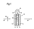
- an optical modulator of the invention comprising Fabry-Perot etalon 10 (not drawn to scale) containing intra-cavity liquid crystal material 12.
- the material 12 is that designated E43, which is nematic material and is commercially available from BDH Chemicals, a British company.
- the liquid crystal material is 10 microns in thickness, a thickness in the range 5-20 microns being suitable.
- the etalon 10 comprises two glass plates 14 each with a respective internal mirror layer 16.
- the mirror layers 16 have reflectivities in the range 85% to 90% and are formed by deposition of silver.
- Each mirror layer bears a respective rubbed polyimide layer 18, which aligns the long axes of the liquid crystal molecules parallel to the plates 14 as indicated by an arrow 20 (homogeneous alignment).
- the mirror layers 16 also act as electrodes for applying an electrical bias field to the liquid crystal material 12. They have electrical connections 22 linking them to an AC voltage source 24 having a frequency of 10 kHz. As is well known in the liquid crystal field, these materials respond to the rms value of an applied AC field, and a frequency in the range 10 Hz to 100 kHz is suitable.
- the etalon 10 is employed to modulate the intensity of an incident light beam 26.
- the etalon beam 26 is polarised as indicated by an arrow 28 parallel to the liquid crystal molecular alignment 20.
- Light transmitted by the etalon 10 is indicated at 30.
- the light beam 26 has an intensity of less than 100 Watt/cm2.
- optical transmission T of the etalon 10 ie the ratio of the transmitted light intensity to that incident, is given by the expression:
- n e is approximately 1.7.
- the voltage source 24 is arranged to provide a 10 kHz signal of magnitude greater than the Freedricks threshold (to be described later) in the liquid crystal material.
- the applied voltage changes the molecular orientation of the material 12, which in the present example (E43) has positive dielectric anisotropy.
- n the refractive index of the material 12 experienced by the incident light beam 26.
- the optical phase change ⁇ in the etalon 10 consequently alters, and so also the etalon transmission T given by Equation (1). T is accordingly tunable by varying the cell voltage.
- etalon transmission T is shown plotted against incident optical wavelength in three graphs 40, 42 and 44 for etalon bias voltages V E of 1.0 V, 0.96 V and 0 respectively.
- V E etalon bias voltage
- the Freedricks threshold occurs at 0.96 V approximately.
- Each of the graphs 40, 42, 44 consists of the well-known Fabry-Perot characteristic of maxima and minima which are regularly spaced as a function of wavelength. It can be seen that maxima of graph 44 are very close to minima of graph 40, and maxima of graph 42 are approximately midway between those of graphs 40 and 44.
- a change of etalon voltage of only 40 mV, 0.96 V to 1.0 V tunes the etalon 10 from a maximum on graph 42 to less than half maximum on graph 40.
- a similar change between graphs 42 and 44 (O V) requires 0.96 V, twenty-four times larger. This illustrates the considerable increase in sensitivity of refractive index to applied voltage produced by increasing the voltage above the Freedricks threshold.
- the refractive index of the liquid crystal material is very sensitive to etalon voltage immediately above the Freedricks threshold or transition, it has been found that the molecular re-orientation required is characterised by a time constant in the range 10-100 milliseconds for E43 and similar nematic materials. This is adequate for conventional liquid crystal displays, but it is unacceptably long for optical signal processing and other optical modulation applications.
- FIG. 3 there is shown a graph 50 of etalon transmission T against etalon rms voltage at an incident wavelength of 632.8 nm.
- the Freedricks voltage V F is shown, this being a little less than one volt in the present example.
- Increasing the etalon voltage above V F tunes T through a series of maxima and minima, which become broader as the voltage increases and the voltage sensitivity of the liquid crystal refractive index reduces. For an applied voltage change from 4 V to 6 V (both well above V F ), transmission changes monotonically from minimum to maximum.
- V A is in fact a square wave, and the rms value is half the peak value as illustrated. It alternates between 5 and 7 volts vms with a cycle time of a little under 12 milliseconds.
- Etalon transmission T responds to V A variation by changing from 0.06 to 0.46. Furthermore, T changes with a response time of 1.08 milliseconds measured between an initial value in switching and a value after switching which is (1-1/e) of its final value.
- a conventional nematic liquid crystal shutter lacking the Fabry-Perot structure would have a response time in the 10-100 millisecond region.
- the combination of a Fabry-Perot structure and a voltage source arranged to switch between voltages both above V F accordingly improves switching time by a factor of between 10 and 100 approximately. This is achieved using voltages compatible with integrated circuit technology, roughly an order of magnitude lower than the prior art of R2. Furthermore, unlike R2, accurate temperature control with power consuming heaters is not required.
- the Freedricks transition is a phenomenon observed in nematic liquid crystal cells. Such cells have a molecular alignment which is imposed by pretreating the surfaces in contact with the liquid crystal material. Thus simple nematic materials such as E43 with positive dielectric anisotropy are employed with so-called homogeneous alignment parallel to cell walls. Other configurations will be described later. By virtue of this alignment, mechanical work must be done on the molecules to reorientate them.
- the Freedricks transition occurs at that voltage at which control of molecular orientation switches from that due to cell wall boundary conditions to that due to applied voltage.
- the Freedricks voltage V F is independent of cell thickness for nematic materials, because the electric field in a cell and the energy required to induce the transition are both inversely proportional to cell thickness.
- the Freedricks transition is defined only for nematic materials and devices such as (a) to (d) above.
- materials such as (e)
- This threshold arises in an analogous fashion to the Freedricks threshold, in that molecular orientation changes from that controlled, by cell or etalon wall boundary conditions to that controlled by applied field.
- the threshold voltage in ferroelectric smectic devices is proportional to cell thickness, so strictly speaking there is a constant threshold electric field rather than a constant threshold voltage. The threshold voltage is however a constant for a given cell.
Landscapes
- Physics & Mathematics (AREA)
- Nonlinear Science (AREA)
- Chemical & Material Sciences (AREA)
- Crystallography & Structural Chemistry (AREA)
- General Physics & Mathematics (AREA)
- Optics & Photonics (AREA)
- Liquid Crystal (AREA)
Claims (10)
- Procédé d'obtention d'une modulation optique, comprenant les étapes suivantes :(a) la réalisation d'un étalon de Fabry-Perot (10) contenant une matière cristalline liquide (12) dans une cavité et des électrodes (16) de polarisation destinées à polariser la matière (12),(b) la circulation, dans l'étalon (10), de lumière (26) d'une intensité insuffisante pour provoquer une bistabilité optique dans la matière (12), et(c) l'application d'une tension de polarisation aux électrodes (16),caractérisé en ce que la matière cristalline liquide (12) qui est utilisée est du type qui possède une tension de seuil VT à laquelle le réglage de l'orientation moléculaire de la matière cristalline liquide (12) commute de celui qui est dû aux conditions aux limites des parois de la cellule à celui qui est dû au champ électrique appliqué et, au-dessus de cette tension de seuil, l'indice de réfraction de la matière (12) est sensible à la polarisation électrique, et en ce que la tension de polarisation est modifiée entre deux valeurs qui sont toutes deux comprises entre VT et 20VT.
- Procédé selon la revendication 1, caractérisé en ce que la tension de polarisation varie entre deux valeurs qui sont toutes deux comprises entre 2VT et 20VT, et entre lesquelles l'étalon (10) présente une transmission optique qui varie de façon monotone.
- Procédé selon la revendication 2, caractérisé en ce que la tension de polarisation est modifiée entre deux valeurs qui sont toutes deux comprises entre 5VT et 10VT.
- Procédé selon la revendication 2 ou 3, caractérisé en ce que l'étalon (10) a une largeur de cavité comprise entre 5 et 20 µm.
- Procédé selon la revendication 4, caractérisé en ce que la matière cristalline liquide (12) est nématique avec une anisotropie diélectrique positive et un alignement homogène par rapport aux parois internes (18) de l'étalon.
- Procédé selon la revendication 4, caractérisé en ce que la matière cristalline liquide (12) a une anisotropie diélectrique négative et un alignement homéotrope incliné par rapport à la perpendiculaire aux parois internes (18) de l'étalon suivant un angle compris entre 2 et 10°.
- Procédé selon la revendication 4, caractérisé en ce que la matière cristalline liquide (12) a une anisotropie diélectrique positive et un alignement moléculaire hybride par rapport aux parois internes (18) de l'étalon.
- Procédé selon la revendication 4, caractérisé en ce que la matière cristalline liquide (12) a une anisotropie diélectrique positive et une torsion d'alignement de cellule π.
- Procédé selon la revendication 4, caractérisé en ce que la matière cristalline liquide (12) a une faible biréfringence et une torsion d'alignement 2π.
- Procédé selon la revendication 2 ou 3, caractérisé en ce que l'étalon (10) a une largeur de cavité comprise entre 1 et 6 µm et la matière cristalline liquide (12) est une matière ferroélectrique smectique ayant un alignement homogène.
Applications Claiming Priority (2)
| Application Number | Priority Date | Filing Date | Title |
|---|---|---|---|
| GB8621438 | 1986-09-05 | ||
| GB868621438A GB8621438D0 (en) | 1986-09-05 | 1986-09-05 | Electro-optic device |
Publications (3)
| Publication Number | Publication Date |
|---|---|
| EP0260073A2 EP0260073A2 (fr) | 1988-03-16 |
| EP0260073A3 EP0260073A3 (en) | 1988-10-05 |
| EP0260073B1 true EP0260073B1 (fr) | 1992-11-11 |
Family
ID=10603736
Family Applications (1)
| Application Number | Title | Priority Date | Filing Date |
|---|---|---|---|
| EP87307812A Expired - Lifetime EP0260073B1 (fr) | 1986-09-05 | 1987-09-04 | Méthode pour l'obtention d'une modulation optique |
Country Status (5)
| Country | Link |
|---|---|
| US (1) | US4779959A (fr) |
| EP (1) | EP0260073B1 (fr) |
| CA (1) | CA1284373C (fr) |
| DE (1) | DE3782592T2 (fr) |
| GB (1) | GB8621438D0 (fr) |
Families Citing this family (103)
| Publication number | Priority date | Publication date | Assignee | Title |
|---|---|---|---|---|
| DE3812334A1 (de) * | 1988-04-14 | 1989-10-26 | Hartmann & Braun Ag | Interferometrische einrichtung |
| GB2219099A (en) * | 1988-05-27 | 1989-11-29 | Stc Plc | Tunable Fabry-Perot filter |
| GB2222464A (en) * | 1988-08-31 | 1990-03-07 | Marconi Gec Ltd | Fabry-perot interferometer |
| JPH02146526A (ja) * | 1988-11-29 | 1990-06-05 | Seiko Instr Inc | 液晶素子 |
| US5076699A (en) * | 1989-05-01 | 1991-12-31 | Rosemount Analytical Inc. | Method and apparatus for remotely and portably measuring a gas of interest |
| EP0494883B1 (fr) * | 1989-10-12 | 1994-07-13 | Hartmann & Braun Aktiengesellschaft | Procede et agencement pour la spectroscopie fabry-perot |
| US5469279A (en) * | 1989-10-30 | 1995-11-21 | The University Of Colorado Foundation, Inc. | Chiral smectic liquid crystal multipass optical filters including a variable retarder (and a variable isotropic spacer) |
| US5381253A (en) * | 1991-11-14 | 1995-01-10 | Board Of Regents Of University Of Colorado | Chiral smectic liquid crystal optical modulators having variable retardation |
| GB8926539D0 (en) * | 1989-11-24 | 1990-10-17 | Secr Defence | Variable frequency dye laser |
| US5111321A (en) * | 1990-10-16 | 1992-05-05 | Bell Communications Research, Inc. | Dual-polarization liquid-crystal etalon filter |
| US5068749A (en) * | 1990-08-31 | 1991-11-26 | Bell Communications Research, Inc. | Electronically tunable polarization-independent liquid crystal optical filter |
| US5132824A (en) * | 1990-08-31 | 1992-07-21 | Bell Communications Research, Inc. | Liquid-crystal modulator array |
| US5150236A (en) * | 1990-08-31 | 1992-09-22 | Bell Communications Research, Inc. | Tunable liquid crystal etalon filter |
| CA2088372C (fr) * | 1990-08-31 | 1999-10-05 | Jayantilal Shamjibhai Patel | Filtre etalon a cristal liquide accordable |
| US5245455A (en) * | 1990-09-10 | 1993-09-14 | Hughes Aircraft Company | Mos light valve with nematic liquid crystal operating in the surface mode |
| US5159481A (en) * | 1990-09-14 | 1992-10-27 | Bell Communications Research, Inc. | Polarization scrambler for polarization-sensitive optical devices |
| US5170271A (en) * | 1991-01-31 | 1992-12-08 | Hughes Aircraft Company | Shaped voltage pulse method for operating a polymer dispersed liquid crystal cell, and light valve employing the same |
| US5321539A (en) * | 1991-02-04 | 1994-06-14 | Nippon Telegraph And Telephone Corporation | Liquid crystal Fabry-Perot etalon with glass spacer |
| US5172257A (en) * | 1991-11-08 | 1992-12-15 | Bell Communications Research, Inc. | Twisted ferroelectric liquid crystal modulator for providing gray scale |
| US5493426A (en) * | 1991-11-14 | 1996-02-20 | University Of Colorado Foundation, Inc. | Lateral electrode smectic liquid crystal devices |
| US5552912A (en) * | 1991-11-14 | 1996-09-03 | Board Of Regents Of The University Of Colorado | Chiral smectic liquid crystal optical modulators |
| US5347377A (en) * | 1992-06-17 | 1994-09-13 | Eastman Kodak Company | Planar waveguide liquid crystal variable retarder |
| US7830587B2 (en) * | 1993-03-17 | 2010-11-09 | Qualcomm Mems Technologies, Inc. | Method and device for modulating light with semiconductor substrate |
| US6674562B1 (en) | 1994-05-05 | 2004-01-06 | Iridigm Display Corporation | Interferometric modulation of radiation |
| US8081369B2 (en) * | 1994-05-05 | 2011-12-20 | Qualcomm Mems Technologies, Inc. | System and method for a MEMS device |
| US5425115A (en) * | 1994-07-18 | 1995-06-13 | Martin Marietta Corporation | Polarization insensitive optical switch |
| US5627666A (en) * | 1994-07-27 | 1997-05-06 | Board Of Regents Of The University Of Colorado | Liquid crystal phase modulator using cholesteric circular polarizers |
| US7898722B2 (en) * | 1995-05-01 | 2011-03-01 | Qualcomm Mems Technologies, Inc. | Microelectromechanical device with restoring electrode |
| US5689314A (en) * | 1995-06-14 | 1997-11-18 | The United States Of America As Represented By The Administrator Of The National Aeronautics And Space Administration | Common path point diffraction interferometer using liquid crystal phase shifting |
| GB9608636D0 (en) * | 1996-04-25 | 1996-07-03 | Secr Defence | A tuneable filter |
| US6211993B1 (en) | 1996-05-20 | 2001-04-03 | Nz Applied Technologies Corporation | Thin film ferroelectric light modulators |
| US6205159B1 (en) | 1997-06-23 | 2001-03-20 | Newport Corporation | Discrete wavelength liquid crystal tuned external cavity diode laser |
| US8928967B2 (en) * | 1998-04-08 | 2015-01-06 | Qualcomm Mems Technologies, Inc. | Method and device for modulating light |
| WO1999052006A2 (fr) | 1998-04-08 | 1999-10-14 | Etalon, Inc. | Modulation interferometrique de rayonnement |
| US6198580B1 (en) | 1998-08-17 | 2001-03-06 | Newport Corporation | Gimballed optical mount |
| KR100284647B1 (ko) * | 1998-11-02 | 2001-03-15 | 김원대 | 네마틱 액정 파브리-페로 파장 가변 필터 장치 |
| US6516130B1 (en) | 1998-12-30 | 2003-02-04 | Newport Corporation | Clip that aligns a fiber optic cable with a laser diode within a fiber optic module |
| FR2790115B1 (fr) | 1999-02-23 | 2001-05-04 | Micro Controle | Procede et dispositif pour deplacer un mobile sur une base montee elastiquement par rapport au sol |
| US6996506B2 (en) | 1999-02-23 | 2006-02-07 | Newport Corporation | Process and device for displacing a moveable unit on a base |
| US6511035B1 (en) | 1999-08-03 | 2003-01-28 | Newport Corporation | Active vibration isolation systems with nonlinear compensation to account for actuator saturation |
| US6686984B1 (en) * | 2000-02-29 | 2004-02-03 | Agilent Technologies, Inc. | Polarization control device |
| DE60133002T2 (de) | 2000-06-27 | 2009-02-26 | Alberta Research Council, Edmonton | Spektrophotometer mit mehreren weglängen |
| US6954253B2 (en) * | 2000-07-25 | 2005-10-11 | Scientific Solutions, Inc. | Optical multiplexer and cross-switch using etched liquid crystal fabry-perot etalons |
| US6655840B2 (en) | 2001-02-13 | 2003-12-02 | Newport Corporation | Stiff cross roller bearing configuration |
| US6601524B2 (en) | 2001-03-28 | 2003-08-05 | Newport Corporation | Translation table with a spring biased dovetail bearing |
| US6791058B2 (en) | 2001-04-25 | 2004-09-14 | Newport Corporation | Automatic laser weld machine for assembling photonic components |
| US6568666B2 (en) | 2001-06-13 | 2003-05-27 | Newport Corporation | Method for providing high vertical damping to pneumatic isolators during large amplitude disturbances of isolated payload |
| US6619611B2 (en) | 2001-07-02 | 2003-09-16 | Newport Corporation | Pneumatic vibration isolator utilizing an elastomeric element for isolation and attenuation of horizontal vibration |
| US7035484B2 (en) * | 2002-04-12 | 2006-04-25 | Xtellus, Inc. | Tunable optical filter |
| US6966535B2 (en) | 2002-05-07 | 2005-11-22 | Newport Corporation | Snubber for pneumatically isolated platforms |
| US6888661B1 (en) | 2002-06-13 | 2005-05-03 | Cheetah Omni, Llc | Square filter function tunable optical devices |
| DE50306222D1 (de) * | 2002-11-15 | 2007-02-15 | Merck Patent Gmbh | Elektrooptisches lichtsteuerelement, elektrooptische anzeige und steuermedium |
| US7002646B2 (en) * | 2003-03-17 | 2006-02-21 | International Business Machines Corporation | Tunable thin film optical devices and fabrication methods for tunable thin film optical devices |
| JP4916647B2 (ja) * | 2003-05-23 | 2012-04-18 | サムスン エレクトロニクス カンパニー リミテッド | 外部共振器半導体レーザーおよびその製造方法 |
| US20050046914A1 (en) * | 2003-08-29 | 2005-03-03 | Gruhlke Russell W. | Wavelength tuning an external cavity laser without mechanical motion |
| US7320455B2 (en) | 2003-10-24 | 2008-01-22 | Newport Corporation | Instrumented platform for vibration-sensitive equipment |
| US7944599B2 (en) | 2004-09-27 | 2011-05-17 | Qualcomm Mems Technologies, Inc. | Electromechanical device with optical function separated from mechanical and electrical function |
| US7304784B2 (en) * | 2004-09-27 | 2007-12-04 | Idc, Llc | Reflective display device having viewable display on both sides |
| US7936497B2 (en) | 2004-09-27 | 2011-05-03 | Qualcomm Mems Technologies, Inc. | MEMS device having deformable membrane characterized by mechanical persistence |
| US7527995B2 (en) * | 2004-09-27 | 2009-05-05 | Qualcomm Mems Technologies, Inc. | Method of making prestructure for MEMS systems |
| US8008736B2 (en) | 2004-09-27 | 2011-08-30 | Qualcomm Mems Technologies, Inc. | Analog interferometric modulator device |
| US7564612B2 (en) | 2004-09-27 | 2009-07-21 | Idc, Llc | Photonic MEMS and structures |
| US7372613B2 (en) | 2004-09-27 | 2008-05-13 | Idc, Llc | Method and device for multistate interferometric light modulation |
| US7289259B2 (en) | 2004-09-27 | 2007-10-30 | Idc, Llc | Conductive bus structure for interferometric modulator array |
| US7420725B2 (en) | 2004-09-27 | 2008-09-02 | Idc, Llc | Device having a conductive light absorbing mask and method for fabricating same |
| US7630119B2 (en) | 2004-09-27 | 2009-12-08 | Qualcomm Mems Technologies, Inc. | Apparatus and method for reducing slippage between structures in an interferometric modulator |
| US8231098B2 (en) | 2004-12-07 | 2012-07-31 | Newport Corporation | Methods and devices for active vibration damping of an optical structure |
| US20060181479A1 (en) * | 2005-02-15 | 2006-08-17 | Mantese Joseph V | Filter assembly and method of filtering electromagnetic radiation |
| US7916980B2 (en) | 2006-01-13 | 2011-03-29 | Qualcomm Mems Technologies, Inc. | Interconnect structure for MEMS device |
| US7953326B2 (en) * | 2006-02-06 | 2011-05-31 | Woods Hole Oceanographic Institution | Systems and methods for underwater optical communication |
| US7649671B2 (en) | 2006-06-01 | 2010-01-19 | Qualcomm Mems Technologies, Inc. | Analog interferometric modulator device with electrostatic actuation and release |
| US7527998B2 (en) | 2006-06-30 | 2009-05-05 | Qualcomm Mems Technologies, Inc. | Method of manufacturing MEMS devices providing air gap control |
| US8115987B2 (en) * | 2007-02-01 | 2012-02-14 | Qualcomm Mems Technologies, Inc. | Modulating the intensity of light from an interferometric reflector |
| US7643202B2 (en) | 2007-05-09 | 2010-01-05 | Qualcomm Mems Technologies, Inc. | Microelectromechanical system having a dielectric movable membrane and a mirror |
| US7630121B2 (en) | 2007-07-02 | 2009-12-08 | Qualcomm Mems Technologies, Inc. | Electromechanical device with optical function separated from mechanical and electrical function |
| WO2009018287A1 (fr) | 2007-07-31 | 2009-02-05 | Qualcomm Mems Technologies, Inc. | Dispositifs pour accentuer la variation de couleur des modulateurs interférométriques |
| KR20100084518A (ko) * | 2007-09-17 | 2010-07-26 | 퀄컴 엠이엠스 테크놀로지스, 인크. | 반투명/반투과반사형 광 간섭계 변조기 장치 |
| US8058549B2 (en) | 2007-10-19 | 2011-11-15 | Qualcomm Mems Technologies, Inc. | Photovoltaic devices with integrated color interferometric film stacks |
| EP2210280A2 (fr) | 2007-10-19 | 2010-07-28 | QUALCOMM MEMS Technologies, Inc. | Dispositif d'affichage équipé d'un dispositif photovoltaïque intégré |
| JP2011504243A (ja) | 2007-10-23 | 2011-02-03 | クォルコム・メムズ・テクノロジーズ・インコーポレーテッド | 調節可能透過型memsベースの装置 |
| US8941631B2 (en) | 2007-11-16 | 2015-01-27 | Qualcomm Mems Technologies, Inc. | Simultaneous light collection and illumination on an active display |
| US8164821B2 (en) | 2008-02-22 | 2012-04-24 | Qualcomm Mems Technologies, Inc. | Microelectromechanical device with thermal expansion balancing layer or stiffening layer |
| US7944604B2 (en) | 2008-03-07 | 2011-05-17 | Qualcomm Mems Technologies, Inc. | Interferometric modulator in transmission mode |
| US7612933B2 (en) | 2008-03-27 | 2009-11-03 | Qualcomm Mems Technologies, Inc. | Microelectromechanical device with spacing layer |
| US8237910B2 (en) * | 2008-04-30 | 2012-08-07 | Kent State University | Polarization independent liquid crystal-based etalon and devices using same |
| US8023167B2 (en) | 2008-06-25 | 2011-09-20 | Qualcomm Mems Technologies, Inc. | Backlight displays |
| US8358266B2 (en) | 2008-09-02 | 2013-01-22 | Qualcomm Mems Technologies, Inc. | Light turning device with prismatic light turning features |
| US8270056B2 (en) | 2009-03-23 | 2012-09-18 | Qualcomm Mems Technologies, Inc. | Display device with openings between sub-pixels and method of making same |
| US8979349B2 (en) | 2009-05-29 | 2015-03-17 | Qualcomm Mems Technologies, Inc. | Illumination devices and methods of fabrication thereof |
| US8270062B2 (en) | 2009-09-17 | 2012-09-18 | Qualcomm Mems Technologies, Inc. | Display device with at least one movable stop element |
| US8488228B2 (en) | 2009-09-28 | 2013-07-16 | Qualcomm Mems Technologies, Inc. | Interferometric display with interferometric reflector |
| US20110169724A1 (en) * | 2010-01-08 | 2011-07-14 | Qualcomm Mems Technologies, Inc. | Interferometric pixel with patterned mechanical layer |
| US20110215344A1 (en) * | 2010-03-05 | 2011-09-08 | Dardy Henry D | LOW POWER GRADED BASE SiGe HBT LIGHT MODULATOR |
| US20110228375A1 (en) * | 2010-03-12 | 2011-09-22 | Mezmeriz, Inc. | Laser illumination module with integrated intensity modulator |
| JP2013524287A (ja) | 2010-04-09 | 2013-06-17 | クォルコム・メムズ・テクノロジーズ・インコーポレーテッド | 電気機械デバイスの機械層及びその形成方法 |
| KR20130091763A (ko) | 2010-08-17 | 2013-08-19 | 퀄컴 엠이엠에스 테크놀로지스, 인크. | 간섭 디스플레이 장치에서의 전하 중성 전극의 작동 및 교정 |
| US9057872B2 (en) | 2010-08-31 | 2015-06-16 | Qualcomm Mems Technologies, Inc. | Dielectric enhanced mirror for IMOD display |
| US8963159B2 (en) | 2011-04-04 | 2015-02-24 | Qualcomm Mems Technologies, Inc. | Pixel via and methods of forming the same |
| US9134527B2 (en) | 2011-04-04 | 2015-09-15 | Qualcomm Mems Technologies, Inc. | Pixel via and methods of forming the same |
| US8659816B2 (en) | 2011-04-25 | 2014-02-25 | Qualcomm Mems Technologies, Inc. | Mechanical layer and methods of making the same |
| US8736939B2 (en) | 2011-11-04 | 2014-05-27 | Qualcomm Mems Technologies, Inc. | Matching layer thin-films for an electromechanical systems reflective display device |
| CN103777381A (zh) * | 2012-10-28 | 2014-05-07 | 天津奇谱光电技术有限公司 | 一种使用液晶相位调制器的可调谐窄带光学滤波设备 |
| DE102015200488A1 (de) * | 2015-01-14 | 2016-07-14 | Fraunhofer-Gesellschaft zur Förderung der angewandten Forschung e.V. | Elektrisch steuerbarer Interferenzfarbfilter und dessen Verwendung |
Citations (1)
| Publication number | Priority date | Publication date | Assignee | Title |
|---|---|---|---|---|
| DE3425584A1 (de) * | 1984-07-11 | 1986-01-16 | Merck Patent Gmbh, 6100 Darmstadt | Optisches system mit einer fluessigkristallzelle, verfahren zu seinem betrieb und seine verwendung |
Family Cites Families (8)
| Publication number | Priority date | Publication date | Assignee | Title |
|---|---|---|---|---|
| US32521A (en) * | 1861-06-11 | W S Kirkham | Lock and knob-latch | |
| US3694053A (en) * | 1971-06-22 | 1972-09-26 | Bell Telephone Labor Inc | Nematic liquid crystal device |
| US3891307A (en) * | 1973-03-20 | 1975-06-24 | Matsushita Electric Industrial Co Ltd | Phase control of the voltages applied to opposite electrodes for a cholesteric to nematic phase transition display |
| USRE32521F1 (en) | 1978-06-08 | 1990-09-18 | James L Fergason | Light modulator demodulator and method of communication employing the same |
| US4444469A (en) * | 1979-06-05 | 1984-04-24 | Beckman Instruments, Inc. | Narrow band rejection filter utilizing a liquid crystal cell |
| US4272195A (en) * | 1979-06-05 | 1981-06-09 | Beckman Instruments, Inc. | Method and apparatus for determining the wavelength of light |
| US4566758A (en) * | 1983-05-09 | 1986-01-28 | Tektronix, Inc. | Rapid starting, high-speed liquid crystal variable optical retarder |
| US4595292A (en) * | 1983-07-29 | 1986-06-17 | The Perkin-Elmer Corporation | Apparatus for detecting coherent radiation and unequal path interferometers |
-
1986
- 1986-09-05 GB GB868621438A patent/GB8621438D0/en active Pending
-
1987
- 1987-09-01 CA CA000545821A patent/CA1284373C/fr not_active Expired - Lifetime
- 1987-09-04 DE DE8787307812T patent/DE3782592T2/de not_active Expired - Fee Related
- 1987-09-04 US US07/093,038 patent/US4779959A/en not_active Expired - Fee Related
- 1987-09-04 EP EP87307812A patent/EP0260073B1/fr not_active Expired - Lifetime
Patent Citations (1)
| Publication number | Priority date | Publication date | Assignee | Title |
|---|---|---|---|---|
| DE3425584A1 (de) * | 1984-07-11 | 1986-01-16 | Merck Patent Gmbh, 6100 Darmstadt | Optisches system mit einer fluessigkristallzelle, verfahren zu seinem betrieb und seine verwendung |
Also Published As
| Publication number | Publication date |
|---|---|
| US4779959A (en) | 1988-10-25 |
| CA1284373C (fr) | 1991-05-21 |
| DE3782592T2 (de) | 1993-05-19 |
| EP0260073A2 (fr) | 1988-03-16 |
| DE3782592D1 (de) | 1992-12-17 |
| GB8621438D0 (en) | 1986-10-15 |
| EP0260073A3 (en) | 1988-10-05 |
Similar Documents
| Publication | Publication Date | Title |
|---|---|---|
| US4779959A (en) | Liquid crystal electro-optic modulator in a fabry-perot interferometer | |
| EP0091661A1 (fr) | Corps de modulation optique à cristaux liquides | |
| US5384067A (en) | Grey scale liquid crystal material | |
| US3912369A (en) | Single polarizer reflective liquid crystal display | |
| US5726723A (en) | Sub-twisted nematic liquid crystal display | |
| KR900008064B1 (ko) | 액정 표시장치 | |
| EP0768562B1 (fr) | Dispositif à cristal liquide et méthode de fabrication d'un dispositif à cristal liquide | |
| EP0091637B1 (fr) | Dispositif d'affichage à cristal liquide | |
| US5453863A (en) | Multistable chiral nematic displays | |
| JPS63115137A (ja) | 液晶ディスプレイ装置 | |
| US4579425A (en) | Multiplexable liquid crystal display with reduced hysteresis | |
| Liang et al. | Dual-frequency addressed variable optical attenuator with submillisecond response time | |
| Matsumoto et al. | Tunable wavelength filter using nano-sized droplets of liquid crystal | |
| JP2005070729A (ja) | 双安定キラルスプレーネマチック液晶表示装置 | |
| US20070139586A1 (en) | Electronically-controllable polarization independent liquid crystal optical medium and devices using same | |
| US6469768B1 (en) | Bistable twisted nematic mode reflective liquid crystal display | |
| JP4942899B2 (ja) | 反射双安定性ディスプレイ装置 | |
| EP0539991A1 (fr) | Dispositif à cristal liquide et dispositif d'affichage | |
| US5604616A (en) | Dual function electro-optical display device exhibiting a bistable image or a fugitive image depending the applied voltage | |
| US5061045A (en) | Liquid crystal light modulation device and liquid crystal light modulation apparatus | |
| Xie et al. | New bistable twisted nematic liquid crystal displays | |
| JPH1195195A (ja) | 高分子分散型液晶表示装置およびその製造方法 | |
| JP3288697B2 (ja) | 電気光学系 | |
| Kim et al. | New configuration of a transflective liquid crystal display having a single cell gap and a single liquid crystal mode | |
| DATE et al. | Reflectivity improvement in holographic polymer dispersed liquid crystal (HPDLC) reflective display devices by controlling alignment |
Legal Events
| Date | Code | Title | Description |
|---|---|---|---|
| PUAI | Public reference made under article 153(3) epc to a published international application that has entered the european phase |
Free format text: ORIGINAL CODE: 0009012 |
|
| AK | Designated contracting states |
Kind code of ref document: A2 Designated state(s): DE FR GB NL |
|
| PUAL | Search report despatched |
Free format text: ORIGINAL CODE: 0009013 |
|
| AK | Designated contracting states |
Kind code of ref document: A3 Designated state(s): DE FR GB NL |
|
| 17P | Request for examination filed |
Effective date: 19890131 |
|
| 17Q | First examination report despatched |
Effective date: 19910306 |
|
| RTI1 | Title (correction) | ||
| GRAA | (expected) grant |
Free format text: ORIGINAL CODE: 0009210 |
|
| AK | Designated contracting states |
Kind code of ref document: B1 Designated state(s): DE FR GB NL |
|
| ET | Fr: translation filed | ||
| REF | Corresponds to: |
Ref document number: 3782592 Country of ref document: DE Date of ref document: 19921217 |
|
| PLBE | No opposition filed within time limit |
Free format text: ORIGINAL CODE: 0009261 |
|
| STAA | Information on the status of an ep patent application or granted ep patent |
Free format text: STATUS: NO OPPOSITION FILED WITHIN TIME LIMIT |
|
| 26N | No opposition filed | ||
| PGFP | Annual fee paid to national office [announced via postgrant information from national office to epo] |
Ref country code: FR Payment date: 19960808 Year of fee payment: 10 |
|
| PGFP | Annual fee paid to national office [announced via postgrant information from national office to epo] |
Ref country code: GB Payment date: 19960820 Year of fee payment: 10 |
|
| PGFP | Annual fee paid to national office [announced via postgrant information from national office to epo] |
Ref country code: DE Payment date: 19960826 Year of fee payment: 10 |
|
| PGFP | Annual fee paid to national office [announced via postgrant information from national office to epo] |
Ref country code: NL Payment date: 19960830 Year of fee payment: 10 |
|
| PG25 | Lapsed in a contracting state [announced via postgrant information from national office to epo] |
Ref country code: GB Free format text: LAPSE BECAUSE OF NON-PAYMENT OF DUE FEES Effective date: 19970904 |
|
| PG25 | Lapsed in a contracting state [announced via postgrant information from national office to epo] |
Ref country code: FR Free format text: THE PATENT HAS BEEN ANNULLED BY A DECISION OF A NATIONAL AUTHORITY Effective date: 19970930 |
|
| PG25 | Lapsed in a contracting state [announced via postgrant information from national office to epo] |
Ref country code: NL Free format text: LAPSE BECAUSE OF NON-PAYMENT OF DUE FEES Effective date: 19980401 |
|
| GBPC | Gb: european patent ceased through non-payment of renewal fee |
Effective date: 19970904 |
|
| NLV4 | Nl: lapsed or anulled due to non-payment of the annual fee |
Effective date: 19980401 |
|
| PG25 | Lapsed in a contracting state [announced via postgrant information from national office to epo] |
Ref country code: DE Free format text: LAPSE BECAUSE OF NON-PAYMENT OF DUE FEES Effective date: 19980603 |
|
| REG | Reference to a national code |
Ref country code: FR Ref legal event code: ST |