EP0260836A2 - Méthode et dispositif pour calibrer une souris électro-optique - Google Patents
Méthode et dispositif pour calibrer une souris électro-optique Download PDFInfo
- Publication number
- EP0260836A2 EP0260836A2 EP87307622A EP87307622A EP0260836A2 EP 0260836 A2 EP0260836 A2 EP 0260836A2 EP 87307622 A EP87307622 A EP 87307622A EP 87307622 A EP87307622 A EP 87307622A EP 0260836 A2 EP0260836 A2 EP 0260836A2
- Authority
- EP
- European Patent Office
- Prior art keywords
- light
- ramped
- predetermined limit
- intensity
- numeric
- Prior art date
- Legal status (The legal status is an assumption and is not a legal conclusion. Google has not performed a legal analysis and makes no representation as to the accuracy of the status listed.)
- Withdrawn
Links
Images




Classifications
-
- G—PHYSICS
- G06—COMPUTING OR CALCULATING; COUNTING
- G06F—ELECTRIC DIGITAL DATA PROCESSING
- G06F15/00—Digital computers in general; Data processing equipment in general
-
- G—PHYSICS
- G06—COMPUTING OR CALCULATING; COUNTING
- G06F—ELECTRIC DIGITAL DATA PROCESSING
- G06F3/00—Input arrangements for transferring data to be processed into a form capable of being handled by the computer; Output arrangements for transferring data from processing unit to output unit, e.g. interface arrangements
- G06F3/01—Input arrangements or combined input and output arrangements for interaction between user and computer
- G06F3/03—Arrangements for converting the position or the displacement of a member into a coded form
- G06F3/0304—Detection arrangements using opto-electronic means
- G06F3/0317—Detection arrangements using opto-electronic means in co-operation with a patterned surface, e.g. absolute position or relative movement detection for an optical mouse or pen positioned with respect to a coded surface
Definitions
- the present invention relates to the field of controlling the movement of a cursor on a cathode ray tube.
- it relates to a method and an apparatus for calibrating an electro-optical transducer, i.e. mouse.
- It is another object to provide a calibration method including the steps of taking a predetermined number of samples of the intensity level of light reflected from a grid to photodetecting means and processing these samples to determine the range of intensity levels.
- Another object of the invention is to provide a calibration routine whereby the time required for carrying out the calibration is reduced.
- a light source emits light at one of a plurality of light intensity levels, which emitted light is reflected from a reflective surface onto four photodetectors fixedly arranged in a square pattern inside the mouse.
- the light source and photodetectors are rigidly fixed inside the housing, which is movable over the reflective surface.
- the pattern on the reflective surface may be a grid of orthogonal or hexagonal lines or curvilinear segments (or a matrix of squares, hexagons, or circles, respectively).
- This pattern is optically imaged onto the four photodetectors by a lens such that the width of a line segment is optically magnified to substantially equal the distance between the centers of adjacent photodetectors.
- the magnified image of the illuminated pattern impinges on the four detectors.
- the photodetectors sense the intensity of light reflected from the grid and generate voltage signals proportional to the changing intensity levels.
- the voltage signals output by the photodetectors are input to four comparators. Each comparator also receives a threshold voltage from a digital-to-analog converter connected to the microprocessor. The threshold voltage is varied in accordance with a predetermined sequence of values during each sampling cycle. Each comparator outputs a predetermined binary digit if the voltage signal from the respective photodetector quadrant exceeds the threshold voltage being supplied.
- the preferred embodiment of the invention can determine whether the photodetector quadrant is receiving reflected light having an intensity level falling in one of four ranges. For each quadrant, the microprocessor receives a two-bit code indicating in which one of the four ranges the intensity level of the quadrant lies.
- the four two-bit codes form an eight-bit code which is hereinafter referred to as the intensity code.
- This eight-bit intensity code is then further processed to determine the position of the mouse relative to the grid pattern.
- the eight-bit intensity code is translated into a two-bit X code and a two-bit Y code representing the approximate location of the mouse relative to a single indicium of the respective grid pattern.
- These X and Y codes are then processed to obtain signals representing unit changes in mouse position in the X and/or Y directions.
- Distance information is obtained by counting signals representing unit changes as a function of direction.
- the X-Y distance and direction information is output to drive a cursor, the position of which is changed in response to the output information.
- the digital-to-analog converter is capable of outputting an analog voltage signal having one of 128 values.
- the microprocessor provides a digital output to the digital-to-analog converter which is ramped in a stepped manner from 0 to 127 (the ascending ramp) N times and then is ramped in a stepped manner from 127 to 0 (the descending ramp) N times for each channel.
- 8N samples are obtained, 2N for each channel.
- the microprocessor determines the maximum and minimum measured intensity values for each channel (i.e. I max and I min ). After each block of N samples, the corresponding stored I max and I min values are tested. If I max is greater than a pre-stored limiting value (i.e. I max.lim ), then the intensity level of the output of the light-emitting means is automatically decremented to the next lower level by the microprocessor. If I min is less than a pre-stored absolute minimum value (i.e. I min.lim then the intensity level of the output of the light-emitting means is automatically incremented to the next higher level. Then another sampling cycle of 8N samples is performed, 2N for each channel, which samples are respectively compared with the stored I max and I min values for each channel. The microprocessor then uses the final values for I max and I min to compute and store the threshold levels for each channel.
- Figure 1 shows the preferred embodiment of a position control system 1, movable over surface 3, in which the calibration arrangement of the invention is incorporated.
- the system 1 comprises a housing 5, a light source 7 and a detecting means 9.
- the light source 7 is powered through conductors 11 and 13.
- Detecting means 9 includes photodector array 15, which receives light reflected from surface 3 and transmitted through imaging lens 17.
- Conductors 19 feed the signal from array 15.
- Light source 7 and detecting means 9 are each rigidly fixed relative to housing 5 by fastening means affixed to internal shelves 21 and 23.
- Housing 5 is provided with low-friction spacers 25 and 27 which elevate the body of the housing, including lens 17 and detecting means 9, above surface 3 by the predetermined distance required to obtain proper focusing of reflected light on the photodetector array.
- Spacers 25 and 27 may be made of a material that will minimize wear of surface 3 and enable the housing 5 to slide easily over that surface.
- source 7 is a light-emitting diode (LED).
- LED light-emitting diode
- Light source 7 emits light that lies preferably in either the red or the infrared portions of the spectrum.
- Light shield 29 prevents light source 7 from illuminating detecting means 9 directly.
- source 7 is mounted so that it is positioned close to surface 3. This will ensure that light emitted by source 7 will impinge on surface 3 at a relatively narrow spot with a higher light intensity than if positioned further away.
- FIG. 2 An alternative preferred embodiment of the optical arrangement can be seen in Fig. 2. Similar elements have the same reference numerals in Figs. 1 and 2. The embodiment depicted in Fig. 2 differs from that of Fig. 1 in that after the light reflected from surface passes through lens 17, it is reflected toward the detecting means 9 by a mirror 8 attached to internal shelf 21.
- the photodetector array 15 comprises four photodetectors, hereinafter referred to as detectors A through D inclusive.
- Photodetector array 15 may be a standard four-quadrant photodetector. As clearly shown in Figs. 6, the detectors comprises the four quadrants of a square photodetector array. Each detector responds independently when radiant energy impinges on its surface area by outputting a voltage proportional to the intensity of the impinging radiant energy.
- Figures 3a and 3b show two possible embodiments of the optically contrasting areas of surface 3. These optically contrasting areas can be applied through conventional printing techniques.
- Both line segments 31 and surface areas 33 can be made of ordinary materials but of contrasting colors.
- white or light-colored paper having black line segments printed thereon is suitable.
- white or light-colored paper having black surfaces printed thereon could be used (see Fig. 3c).
- a sheet of transparent photographic film with black line segments spaced thereon can be placed on a reflective surface.
- a sheet of transparent photographic film with black surface areas spaced therein could alternatively be placed on such a reflective surface.
- each line segment has a width equal to one arbitrary unit and each square area has sides with a length equal to two arbitrary units.
- line segments 31 define hexagonal areas 33.
- surface areas 33 may be circular.
- the optically contrasting pattern of segments 31 and surface areas 33 is optically imaged onto the detectors A through D of the photodetector array 15.
- the imaging lens 17 magnifies the image of the surface so that the width of a segment 31 is magnified to approximately equal the distance between centers of detector quadrants when the image impinges on the detector array 15. For example, if segments 31 have a width of 0.01 inch and the spacing between quadrant centers is 0.05 inch, then a magnification of 5 ⁇ would be required.
- the photodetector 15 detects reflected radiant energy from the grid pattern 31, 33 of Fig. 3a
- the photodetector "views" the pattern shown in Fig. 3d due to the fact that the optical lens is non-ideal.
- the grid pattern of Fig. 3d represents the view as seen by the photodetector
- the grid pattern of Fig. 3a represents the view as seen by the human eye.
- the "view" of the grid pattern is distorted as the result of passage of the radiant energy through a non-ideal, i.e. degraded, lens.
- the optical mouse of the present invention is provided with tables of data which serve to compensate for this distortion, enabling accurate position determination.
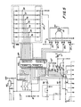
- the common cathode 35 of photodetector array 15 is connected to a +5-volt power supply (not shown).
- the anodes of detectors A through D are respectively electrically connected to the positive input ports of the corresponding comparators 37, 39, 41 and 43.
- These comparators could each be of the LM339N type.
- Each comparator has two input ports and an output port.
- the output ports of these comparators are respectively connected to pins 21 through 24 of microprocessor 45.
- the microprocessor is preferably of the 8051/8751 type.
- Resistors R21, R23, R25 and R27 are respectively connected to junctions lying between the positive input ports of the comparators and the anodes of the photodetector. These resistors are connected to ground and each have a resistance of 1.0 M ⁇ in the preferred embodiment.
- the negative input ports of comparators 37, 39, 41 and 43 are connected in common to the output of digital-to-analog converter 47.
- the digital-to-analog converter comprises an array of resistors R2-R8 and R10-R16 connected across a pair of junctions 49 and 51.
- the array comprises pairs of resistors connected in series (R2/R10,...R8/R16), with the seven pairs of resistors in turn being connected in parallel across the junctions 49, 51.
- the junctions 52-58 respectively arranged between the pairs of series-connected resistors are in turn respectively electrically connected to pins 33-39 of microprocessor 45.
- Junction 49 is connected to ground by way of resistor R17 (39 k ⁇ ) as well as to the negative input ports of comparators 37, 39, 41 and 43, and junction 51 is connected to a +5-volt power supply.
- Pin 31 of the microprocessor is connected to junction 51 by way of ferrite bead L1, as is pin 40.
- the microprocessor 45 is electrically connected to light source 7 by way of inverters 61, 63 and 65 and respective resistors R26, R24 and R22.
- the input ports of inverters 61, 63 and 65 are respectively connected to pins 15, 16 and 17 of the microprocessor.
- the light source 7 is preferably an infrared light-emitting diode (type DS1).
- Light source 7 and resistor R28 (150 ⁇ ) are series-connected across a +5-volt power supply.
- Inverters 61, 63 and 65 are respectively biased by resistors R33, R34, and R35.
- Light source 7 is controlled by microprocessor 45 through inverters 61, 63 and 65.
- the light-emitting diode 7 can emit any one of eight possible light intensities depending on the three-bit command output by microprocessor 45 at ports 15-17.
- the clock 67 is connected to pins 18 and 19 of microprocessor 45.
- the voltage regulator 62 is electrically connected to junction 60, which is in turn connected to pin 20 (GND) of microprocessor 45 and to junction 59 by way of capacitor C3.
- Junction 59 is electrically connected to pin 40 (VCC).
- the receive (RCV) and transmit (XMIT) terminals which are connected to the host, are operatively coupled to pins 10 and 11 respectively of microprocessor 45 by way of inverters 79 and 77 respectively.
- the reset terminal (i.e. pin 9) of microprocessor 45 is connected to junction 69.
- a capacitor C4 and resistor R9 are series-connected across a +5-volt source, with junction 69 situated between the capacitor and resistor.
- housing 5 is gripped by the operator's hand and moved in any direction by sliding over the surface 3.
- Source 7 is positioned so that the emitted light impinges on surface 3. The light is then reflected if it impinges on reflective areas 33 or is absorbed if it impinges on non-reflective line segments 31.
- Detecting means 9 is positioned so that light emitted by source 7 and reflected by areas 33 is then detected by photodetector array 15.
- Each detector of array 15 detects light independently, outputting a voltage signal proportional to the amount of light impinging on its surface.
- Detector A outputs a signal to comparator 37, detector B to comparator 39, detector C to comparator 41, and detector D to comparator 43.
- Each comparator switches when the output voltage of the corresponding photodetector crosses the respective threshold voltage being input from the digital-to-analog converter 47.
- the output ports of the comparators 37, 39, 41, 43 are connected to the microprocessor 45, which reads the output pattern at a regular rate.
- Each comparator output will either be a voltage signal representing that the respective detector output voltage is greater than or equal to the threshold voltage or a voltage signal representing that the respective detector output voltage is less than the threshold voltage.
- the output signal from each comparator has one of two voltage levels, which voltage levels the microprocessor treats as binary signals, e.g. "1" or "0". These binary signals are processed to obtain information regarding the movement of the mouse relative to the grid pattern as reflected in the varying outputs of the detector quadrants. For each sampling cycle, the microprocessor receives two bits from each comparator, thereby forming the eight-bit intensity code. The details of the thresholding procedure will be discussed further below.
- Figs. 6b-6d, 6f-6h and 6j-6l depict the so-called "movement legal" positions of the optical mouse relative to the grid pattern. There are a total of nine possible “movement legal" positions for each indicium.
- Figs. 6b, 6c and 6d show movement of the mouse from left to right.
- the movement of the mouse from the position in Fig. 6b to the position in Fig. 6c constitutes a boundary crossing, i.e. detector A crosses the boundary between a first non-reflective line segment 31 ⁇ and a first reflective surface area 33 ⁇ .
- the movement of the mouse from the position in Fig. 6c to the position in Fig. 6d constitutes another boundary crossing, i.e.
- detector D crosses the boundary between the first reflective surface area and a second non-reflective line segment.
- the movement of the mouse from the position in Fig. 6d to the position in Fig. 6b also constitutes a boundary crossing, i.e. detectors A and D both cross boundaries -- detector A crossing from the first reflective surface area to the second non-reflective line segment and detector D crossing from the second non-reflective line segment to a second reflective surface area.
- the movement of the mouse from the position in Fig. 6b to the position in Fig. 6f constitutes a boundary crossing, and so forth for each of the rows and columns depicted in Figs. 6b-6d, 6f-6h and 6j-6l.
- the movement between "movement legal” positions i.e. the boundary crossings, are indicated by changes in the photodetector output voltages. These output voltages are processed by the circuitry of Fig. 5 to determine the direction of each boundary crossing and then count up or down by unity for each boundary crossing.
- the running count represents the absolute position of the mouse relative to a starting position.
- Figs. 6 Each of the positions depicted in Figs. 6 is assigned a corresponding two-bit X code and a corresponding two-bit Y code.
- the X codes differ by only one bit for horizontally adjacent positions in Figs. 6, while the Y codes differ by only one bit for vertically adjacent positions.
- Figs. 6a, 6e, 6i and 6m show the sequence of positions during travel of the photodetector "view" along a vertical line.
- Figs. 6m-6q shown the sequence of positions during travel along a horizontal line.
- this travel of the photodetector "view" whereby at least two adjacent quadrants overlie a line during travel, will hereinafter be referred to as "riding”.
- the condition wherein the "view" of a quadrant overlies a boundary will hereinafter be referred to as "straddling.”
- the photodetector output voltages are ambiguous when the photodetector is sensing the square areas indicated by A-D in Figs. 6e and 6p.
- the output voltages are ambiguous in the sense that they are identical for the two straddle positions respectively shown in Figs. 6e and 6p. Therefore, it is not possible to determine which of the two positions is being occupied by the mouse without further processing of the photodetector output voltages.
- the microprocessor 45 can only determine that the mouse is in one of the two positions. Hence the photodetector output voltages are ambiguous.
- the mouse achieves a four-level resolution by utilizing a thresholding technique whereby the threshold voltage supplied to comparators 37, 39, 41 and 43 can take on three possible values for each quadrant. These values are unique for each quadrant and are determined in accordance with the calibration procedure described hereinafter.
- the variations in the exact threshold levels for respective quadrants reflect the fact that differences arise in the characteristics of each quadrant during the manufacturing process. In other words, no two quadrants are identical. Since each of the four quadrants will have three threshold levels associated therewith, there will be a total of 12 threshold levels stored in the internal random access memory of the microprocessor. These threshold levels are obtained as the result of the calibration.
- the threshold voltages for each quadrant are output to the comparators in accordance with the following pattern: (a) the microprocessor 45 outputs the digital value corresponding to the intermediate threshold level to the D/A converter 47; (b) if the corresponding comparator output indicates that the quadrant output voltage is less than the intermediate threshold voltage, then the microprocessor next outputs the digital value corresponding to the lowest threshold level; (c) if the corresponding comparator output indicates that the quadrant output voltage is equal to or greater than the intermediate threshold voltage, then the microprocessor next outputs the digital value corresponding to the highest threshold level.
- the intensity range of the quadrant output can be determined by a two-stage three-level thresholding technique, wherein the threshold voltage which is applied during the second thresholding step for each quadrant will depend on the results of the first thresholding step.
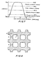
- the threshold voltages output by digital-to-analog converter 47 correspond to the threshold intensity levels shown in the graph of Fig. 7.
- each quadrant of the photodetector outputs a voltage substantially proportional to the amount, i.e. intensity, of reflected light impinging on the quadrant.
- the graph in Fig. 7 shows the magnitude of the impinging light intensity for a single quadrant of the photodetector as the mouse translates (without "riding" a line) across three consecutive grid units in either the X or Y direction (recall that a grid unit equals the width of a line segment 31).
- the solid curve represents the theoretical intensity under ideal conditions, whereas the dashed portions represent the actual intensity, which diverges from the theoretical.
- the intensity of impinging light is given as a percentage of an intensity I cal , which is the range of intensity measured during the calibration procedure.
- the quantity I cal represents the difference between the maximum and minimum intensities detected during sampling in accordance with the calibration routine, i.e. I cal I max - I min .
- the minimum intensity I min is due to leakage light impinging on the photodetector quadrant and a voltage produced by the hardware itself as the result of bias current in the photodectector.
- the light intensity detected by a photodetector quadrant theoretically varies from a value substantially equal to zero when the view of the quadrant entirely overlies a non-reflective line segment to a peak value when the view of the same quadrant entirely overlies a reflective surface area.
- the light intensity when a single quadrant totally overlies a line will be about I min + .10I cal due to the aforementioned leakage light and bias current (I min ) and optical phenomena such as diffraction (.1OI cal ).
- the mouse of the invention is able to detect within which of four intensity ranges the quadrant voltage output, proportional to light intensity, lies.
- the microprocessor performs the calibration procedure as part of an initialization routine. First, the microprocessor takes a predetermined number of samples for each channel (i.e. for each quadrant and corresponding comparator) while the mouse is moved randomly over the grid surface. The sample photodetector outputs are processed by the microprocessor to obtain I min and I max for each channel. Then the microprocesor calculates the threshold values I min + .16(I max - I min ), I min + .46(I max - I min ) and I min + .74(I max - I min ) for each channel. Each of these threshold values is stored as a seven-bit code in the internal random access memory of the microprocessor.
- the digitization routine is begun.
- the photodetector outputs are sampled to form an eight-bit intensity code representing the intensity values of the light being detected by the four quadrants of the detector at a particular position.
- an eight-bit intensity code could correspond to one of 256 possible values.
- the microprocessor forms this eight-bit intensity code by processing the eight bits of information received from the comparators during one thresholding cycle.
- the eight bits correspond to the two separate outputs obtained from each of the four comparators when the respective intermediate and either highest or lowest threshold voltages are successively output by the digital-to-analog converter. These analog threshold voltages are output in response to the output of the respective digital threshold values by the microprocessor.
- the resulting eight-bit intensity code comprises four two-bit codes, each two-bit code (hereinafter referred to as "quadrant intensity code") representing the intensity range in which the light impinging on the corresponding photodetector quadrant falls. For example, if the intensity of light impinging on a quadrant lies in the first intensity range (see Fig. 7), then the corresponding comparator output will be low for both samples and the microprocessor will store the two-bit binary code 00 at the appropriate address in internal RAM. If the intensity is in the second intensity range, then the binary code 01 is stored. If the intensity is in the third intensity range, then the binary code 10 is stored. And lastly, if the intensity is in the fourth intensity range, then the binary code 11 is stored.
- quadrant intensity code each two-bit code representing the intensity range in which the light impinging on the corresponding photodetector quadrant falls. For example, if the intensity of light impinging on a quadrant lies in the first intensity range (see Fig. 7), then the corresponding comparat
- a two-bit intensity code is stored for each quadrant of the photodetector, thereby forming an eight-bit word (i.e. intensity code) representing the amounts of light impinging on the respective photodetector quadrants.
- This eight-bit intensity code then undergoes further processing by the microprocessor to determine the direction of incremental (i.e. one grid unit) movements of the mouse along the X and Y axes, as described in detail in the aforementioned co-pending U.S. patent application Ser. No. 860,231.
- Fig. 8 generally illustrates a small portion of a sampling cycle.
- the microprocessor 45 repeatedly outputs ramped digital signals to the digital-to-analog converter (DAC) 47.
- the ramps of digital signals take two forms: ascending ramps and descending ramps.
- the microprocessor For the ascending ramps, the microprocessor begins by outputting a digital value of zero and then successively incrementing the output digital value by unity until the comparator being sampled switches to output a "0", indicating that the corresponding quadrant output voltage has become less than the DAC output voltage in response to the most recent increment by unity.
- the digital values are successively stored in an internal register and output therefrom by the microprocessor to the digital-to-analog converter.
- the ramped values are generated by sending signals to the register which increment the count in the register by unity at a predetermined clocking rate.
- a typical stepped ascending ramped DAC output voltage is shown in Fig. 8, beginning at time t a1 and ending at time t a2 .
- the microprocessor stores the intensity value I1 in response to the voltage ramp crossing the curve representing the quadrant output voltage, as described in detail below.
- the microprocessor then repeats this ramping operation to obtain I2 by again outputting a digital value of zero at time t a2 and thereafter successively incrementing the output digital value by unity until the comparator being sampled again switches to output a "0".
- This ascending ramping operation is repeated N times for each channel to obtain a block of measured intensity values I1 to I N .
- the ramps are supplied at a frequency such that the mouse can be moved only incrementally in the time interval between successive ramps.
- the microprocessor For the descending ramp, the microprocessor begins by outputting a digital value 127 from an internal register and then successively decrementing the digital value stored in the register by unity until the comparator being sampled switches to output a "1" when the register contents are output, indicating that the corresponding quadrant output voltage has become greater than the DAC output voltage in response to the most recent decrement by unity.
- a typical stepped descending ramped DAC output voltage is shown in Fig. 8, beginning at time t d1 and ending at time t d2 .
- the ascending ramps the descending ramping operation is repeated N times for each channel to obtain a series of measured intensity values I N+1 to I 2N .
- the microprocessor determines the values I max and I min , as previously described. This is accomplished by storing the measured intensity value I1 (see Fig. 8) in a register IMAX and in a register IMIN after the first ascending ramp and then comparing the measured intensity value I2 with the stored value I1 after the second ascending ramp. If I2 > I1, then I2 is stored in register IMAX in place of I1 and the value stored in register IMIN remains unchanged. If I2 ⁇ I1 , then I2 is stored in register IMIN in place of I1 and the value stored in register IMAX remains unchanged. Next the measured intensity value I3 is compared with the values stored in the IMAX and IMIN registers after the third ascending ramp has been halted.
- the values stored in registers IMAX and IMIN are respectively compared with the values of I max.lim and I min.lim , which in the preferred embodiment are respectively equal to intensity values of 121 and 12 on a scale from 0 to 127. If I max > I max.lim , then the LED intensity level is adjusted to the next lower level and the sampling cycle is begun anew. If I min ⁇ I min.lim , then the LED intensity level is adjusted to the next higher level and the sampling cycle is begun anew. If I max ⁇ I max.lim and I min ⁇ I min.lim , then no adjustment of the LED intensity level is necessary.
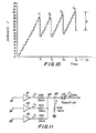
- FIG. 9 Sample waveform A for one of the channels is shown as falling below I min.lim .
- the microprocessor 45 compares I min with I min.lim and I max with I max.lim . Because I min is less than I min.lim (i.e. 12).
- the intensity level of the LED 7 is adjusted to the next higher level, following which another block of N samples are acquired for the same channel. This adjustment of the LED intensity level is reflected in a shifting of the waveform upward. If the waveform is shifted upward into the acceptable range, i.e. between I min.lim and I max.lim (see waveform B in Fig. 9, which is shifted upward with respect to waveform A), then no further adjustment of the LED intensity is necessary.
- the intensity of LED 7 is dependent on the current I total which flows therethrough.
- the current I total in turn depends on whether currents are flowing through the inverters 61, 63 and 65 which are arranged in parallel between junction 87 and the microprocessor 45.
- Junction 87 is connected to the negative terminal of LED 7 by way of junction 89, which is connected to ground by way of resistor R28 (150 ⁇ ).
- a current I1 flows through resistor R28.
- the inverters 61, 63 and 65 are respectively connected to junction 87 by way of resistors R26 (820 ⁇ ), R24 (390 ⁇ ), and R22 (200 ⁇ ), and are respectively connected to pins 15, 16 and 17 of microprocessor by way of junctions 81, 83 and 85. Junctions 81, 83 and 85 are in turn connected to a +5 voltage source by way of resistors R33, R34 and R35 of resistor array 91.
- the amount of current I total is determined by a three-bit code output from pins 15-17 of microprocessor 45. Each bit of this three-bit code switches on the corresponding inverter. For example, if the microprocessor outputs a "1" at pin 15, the microprocessor acts as a source of bias current for switching on the transistor inside inverter 61. However, because the current supplied by the microprocessor is barely sufficient to bias the transistor, an additional current is provided to inverter 61 from resistor R33. In response to sufficient bias current, inverter 61 acts as a current sink, resulting in a flow of current I2 through resistor R26 and toward inverter 61. When the microprocessor outputs a "0" at pin 15, the microprocessor acts as a current sink. Therefore, all of the current from resistor R33 flows toward the microprocessor and accordingly inverter 61 is not biased, i.e. receives no bias current.
- a "1" output at pin 16 of microprocessor 45 produces a current I3 flowing through resistor R24 and toward inverter 63 and a "1" output at pin 17 produces a current I4 flowing through resistor R22 and toward inverter 65.
- the following table shows the dependence of I total on the three-bit code output by microprocessor 45 via pins 15, 16 and 17.
- I1 23.3 mA
- I2 4.27 mA
- I3 8.97 mA
- I4 17.5 mA
- the object of adjusting the LED intensity in the foregoing manner is to obtain I max and I min values for each of the channels A-D which fall within the acceptable range, i.e. between I max.lim and I min.lim .
- I ref2 I min + .46I cal
- I ref3 I min + .74I cal
- I cal I max - I min .
- the foregoing calibration sub-routine is carried out as part of the mouse initialization routine.
- the LED intensity can be adjusted as necessary to compensate for any change in the LED performance due to aging.
- the microprocessor will output a signal for activating a warning light (not shown) to indicate a failure condition.
- FIG. 10 A second preferred embodiment of the method in accordance with the invention is partially depicted in Fig. 10.
- the ramping can be modified such that the microprocessor 45 outputs successive digital values to digital-to-analog convertor 47 which are incremented by a value of two each step.
- I max is actually 113 at a given sampled instant, and if the ascending ramps comprise even digital values (i.e. 0, 2, 4, 6...), then at the instant when I max is being sampled the corresponding comparator will be triggered only after the output of the microprocessor has gone from 112 to 114.
- the microprocessor will store a value of 114 when in actuality the intensity level was 113.
- the descending ramps comprise only odd digital values (i.e., 127, 125, 123, 121). Therefore, although the microprocessor has stored a value of I max equal to 114 as a result of the block of ascending ramp samples, the descending ramps will trigger the comparator at a value of 113 when the I max value is being sampled.
- the error inherent in ramping in steps of two is eliminated by using ascending ramps with even digital values and descending ramps with odd digital values. Alternatively, one could use ascending ramps with odd digital values and descending ramps with even digital values.
- the current ramp value stored in a register in internal memory must be transferred to the arithmetic unit inside the microprocessor.
- the arithmetic unit adds 2 to the digital ramp value received and then transfers the incremented value back to the same register, from where it is output to the DAC 47.
- an ascending ramp can be output having step values of 2.
- the arithmetic unit must subtract 2 from the register contents.
- the ramping operation can be speeded up even further by increasing the stepping value to 3 or more, at the cost of decreased accuracy however.
- the ramping operation can be speeded up further by starting the first ascending ramp of each block at 2 and starting subsequent ascending ramps at values which are less than the measured intensity values by a predetermined amount ⁇ .
- the subsequent ascending ramps require less time to trigger the comparator whose output is being sampled since the steps from 0 to I n - ⁇ are eliminated, with corresponding time savings.
- ⁇ 12.
- the microprocessor tests the acquired I max and I min values for each channel to determine whether I max > I max.lim (i.e. 121) and whether I min ⁇ I min.lim (i.e. 120). In addition, the microprocessor also calculates and tests the value I max - I min in accordance with stored program instructions. It should be pointed out that the range I max - I min increases as I min increases. The microprocessor is programmed to maintain I max - I min within a predetermined range. On the one hand, if I max - I min > 105, then the LED intensity will be automatically adjusted to the next lower level. On the other hand, if I max - I min ⁇ 35, the LED intensity will be adjusted to the next higher level. These checks ensure a signal that can be processed with acceptable margins of error.
Landscapes
- Engineering & Computer Science (AREA)
- Theoretical Computer Science (AREA)
- General Engineering & Computer Science (AREA)
- Physics & Mathematics (AREA)
- General Physics & Mathematics (AREA)
- Human Computer Interaction (AREA)
- Computer Hardware Design (AREA)
- Position Input By Displaying (AREA)
Applications Claiming Priority (2)
| Application Number | Priority Date | Filing Date | Title |
|---|---|---|---|
| US06/909,829 US4807166A (en) | 1986-09-19 | 1986-09-19 | Method and apparatus for calibrating an electro-optical mouse |
| US909829 | 1986-09-19 |
Publications (2)
| Publication Number | Publication Date |
|---|---|
| EP0260836A2 true EP0260836A2 (fr) | 1988-03-23 |
| EP0260836A3 EP0260836A3 (fr) | 1989-07-26 |
Family
ID=25427895
Family Applications (1)
| Application Number | Title | Priority Date | Filing Date |
|---|---|---|---|
| EP87307622A Withdrawn EP0260836A3 (fr) | 1986-09-19 | 1987-08-27 | Méthode et dispositif pour calibrer une souris électro-optique |
Country Status (5)
| Country | Link |
|---|---|
| US (1) | US4807166A (fr) |
| EP (1) | EP0260836A3 (fr) |
| JP (1) | JPS63163919A (fr) |
| KR (1) | KR880004386A (fr) |
| BR (1) | BR8704821A (fr) |
Cited By (2)
| Publication number | Priority date | Publication date | Assignee | Title |
|---|---|---|---|---|
| CN1086236C (zh) * | 1997-10-06 | 2002-06-12 | 盛群半导体股份有限公司 | 电脑鼠标光藕合输入讯号自动检测装置 |
| EP1339011A1 (fr) * | 2002-02-14 | 2003-08-27 | Unity Opto Technology Co., Ltd. | Souris optique pour un ordinateur personnel |
Families Citing this family (20)
| Publication number | Priority date | Publication date | Assignee | Title |
|---|---|---|---|---|
| US4912672A (en) * | 1988-01-15 | 1990-03-27 | Giorgio Paul J | Computer peripheral rate aided sensing system |
| US4908791A (en) * | 1988-01-15 | 1990-03-13 | Giorgio Paul J | Switch display encoder apparatus |
| US4979135A (en) * | 1988-01-27 | 1990-12-18 | Storage Technology Corporation | Vision system illumination calibration apparatus |
| US5086404A (en) * | 1988-09-02 | 1992-02-04 | Claussen Claus Frenz | Device for simultaneous continuous and separate recording and measurement of head and body movements during standing, walking and stepping |
| US5083288A (en) * | 1989-02-24 | 1992-01-21 | Arpad Somlyody | Apparatus for configuring a remote process sensor and signal transmitter |
| WO1991020022A1 (fr) * | 1990-06-14 | 1991-12-26 | Multicoin Australia Pty. Ltd. | Ameliorations relatives a des ensembles manettes de jeu |
| GB9119092D0 (en) * | 1991-09-06 | 1991-10-23 | Sarnoff David Res Center | Optomechanical keyboard |
| US5541623A (en) * | 1993-06-02 | 1996-07-30 | Alps Electric (U.S.A.) Inc. | Temperature compensated opto-electronic circuit and mouse using same |
| US6727887B1 (en) * | 1995-01-05 | 2004-04-27 | International Business Machines Corporation | Wireless pointing device for remote cursor control |
| US5623284A (en) * | 1995-04-18 | 1997-04-22 | Elan Microelectronics Corporation | Input device controller |
| US6950094B2 (en) | 1998-03-30 | 2005-09-27 | Agilent Technologies, Inc | Seeing eye mouse for a computer system |
| US6396005B2 (en) | 1998-06-15 | 2002-05-28 | Rodgers Technology Center, Inc. | Method and apparatus for diminishing grid complexity in a tablet |
| US6225621B1 (en) * | 1999-05-07 | 2001-05-01 | Automatic Timing & Controls, Inc. | Laser photoelectric sensor |
| US6455840B1 (en) * | 1999-10-28 | 2002-09-24 | Hewlett-Packard Company | Predictive and pulsed illumination of a surface in a micro-texture navigation technique |
| US6552713B1 (en) | 1999-12-16 | 2003-04-22 | Hewlett-Packard Company | Optical pointing device |
| US6774351B2 (en) * | 2001-05-25 | 2004-08-10 | Agilent Technologies, Inc. | Low-power surface for an optical sensor |
| TW576534U (en) * | 2003-04-23 | 2004-02-11 | Sunplus Technology Co Ltd | Light-guiding apparatus of optical mouse |
| US7399953B2 (en) * | 2005-05-06 | 2008-07-15 | Avago Technologies Ecbu Ip Pte Ltd | Light source control in optical pointing device |
| TW201816557A (zh) * | 2016-10-26 | 2018-05-01 | 原相科技股份有限公司 | 可施行光學移動品質判斷方法的電腦可讀取記錄媒體以及使用此光學移動品質判斷方法的光學移動偵測裝置 |
| CN108021244A (zh) * | 2016-11-03 | 2018-05-11 | 原相科技股份有限公司 | 一种光学移动品质判断方法以及光学移动品质判断系统 |
Family Cites Families (16)
| Publication number | Priority date | Publication date | Assignee | Title |
|---|---|---|---|---|
| DE2214658C3 (de) * | 1972-03-25 | 1974-12-19 | Licentia Patent-Verwaltungs-Gmbh, 6000 Frankfurt | Schaltung zur Schwellenwertbüdung |
| US4157533A (en) * | 1977-11-25 | 1979-06-05 | Recognition Equipment Incorporated | Independent channel automatic gain control for self-scanning photocell array |
| US4364035A (en) * | 1981-05-18 | 1982-12-14 | Kirsch Steven T | Electro-optical mouse |
| US4390873A (en) * | 1981-05-18 | 1983-06-28 | Kirsch Steven T | Electronic mouse |
| US4521772A (en) * | 1981-08-28 | 1985-06-04 | Xerox Corporation | Cursor control device |
| JPS5886670A (ja) * | 1981-08-29 | 1983-05-24 | Pentel Kk | タブレツト入力装置 |
| US4409479A (en) * | 1981-12-03 | 1983-10-11 | Xerox Corporation | Optical cursor control device |
| US4550250A (en) * | 1983-11-14 | 1985-10-29 | Hei, Inc. | Cordless digital graphics input device |
| US4710759A (en) * | 1984-02-22 | 1987-12-01 | Zenith Electronics Corporation | Interactive CRT with touch level set |
| DE3506309A1 (de) * | 1984-02-22 | 1985-08-22 | Summagraphics Corp | Elektro-optische maus |
| JPS60251479A (ja) * | 1984-05-28 | 1985-12-12 | Brother Ind Ltd | 光学マ−ク読み取り装置 |
| JP2683699B2 (ja) * | 1984-06-18 | 1997-12-03 | アンプ インコーポレーテッド | タッチ入力装置 |
| US4631675A (en) * | 1984-07-20 | 1986-12-23 | Honeywell Inc. | Automatic light-intensity control |
| US4707689A (en) * | 1985-03-25 | 1987-11-17 | AT&T Information Systems Inc. American Telephone & Telegraph Company | Adaptive thresholding scheme for optically-based touch screens |
| US4710758A (en) * | 1985-04-26 | 1987-12-01 | Westinghouse Electric Corp. | Automatic touch screen calibration method |
| US4857903A (en) * | 1986-05-06 | 1989-08-15 | Summagraphics Corporation | Electro-optical mouse with improved resolution for compensation of optical distortion |
-
1986
- 1986-09-19 US US06/909,829 patent/US4807166A/en not_active Expired - Fee Related
-
1987
- 1987-08-26 KR KR870009340A patent/KR880004386A/ko not_active Withdrawn
- 1987-08-27 EP EP87307622A patent/EP0260836A3/fr not_active Withdrawn
- 1987-09-18 BR BR8704821A patent/BR8704821A/pt unknown
- 1987-09-19 JP JP62233757A patent/JPS63163919A/ja active Pending
Cited By (2)
| Publication number | Priority date | Publication date | Assignee | Title |
|---|---|---|---|---|
| CN1086236C (zh) * | 1997-10-06 | 2002-06-12 | 盛群半导体股份有限公司 | 电脑鼠标光藕合输入讯号自动检测装置 |
| EP1339011A1 (fr) * | 2002-02-14 | 2003-08-27 | Unity Opto Technology Co., Ltd. | Souris optique pour un ordinateur personnel |
Also Published As
| Publication number | Publication date |
|---|---|
| KR880004386A (ko) | 1988-06-03 |
| JPS63163919A (ja) | 1988-07-07 |
| EP0260836A3 (fr) | 1989-07-26 |
| US4807166A (en) | 1989-02-21 |
| BR8704821A (pt) | 1988-05-17 |
Similar Documents
| Publication | Publication Date | Title |
|---|---|---|
| US4807166A (en) | Method and apparatus for calibrating an electro-optical mouse | |
| US4403859A (en) | Photoelectric incremental measuring apparatus | |
| US4110610A (en) | Digital electrical position transducer | |
| US5266810A (en) | Package height detector having a first group of light sensors selectively enabled by the detector outputs of a second group of light sensors | |
| US5235181A (en) | Absolute position detector for an apparatus for measuring linear angular values | |
| US4857903A (en) | Electro-optical mouse with improved resolution for compensation of optical distortion | |
| JP3400485B2 (ja) | 光学式位置検出装置および光学式座標入力装置 | |
| EP0042179B1 (fr) | Codeur | |
| EP0503716B1 (fr) | Dispositif de mesure pour déterminer une position absolue d'un élément mobile et élément d'échelle convenant dans un tel instrument de mesure | |
| US4712100A (en) | Coordinate inputting apparatus using multiple sensors | |
| US4668862A (en) | Method and apparatus for determining measured quantities with a centroid detecting encoder | |
| US4421980A (en) | Position encoder with closed-ring diode array | |
| EP0290140B1 (fr) | Equipement pour mesurer des différences de niveau | |
| JPS6019441B2 (ja) | フオトセルパタ−ン感知装置の検出回路 | |
| WO1990002347A1 (fr) | Systeme de detection ameliore pour souris optique | |
| EP3736543B1 (fr) | Lecteurs optiques | |
| US6438860B1 (en) | Device and process for determining position between two parts which are movable relative to one another | |
| US4122438A (en) | Position encoding arrangements | |
| JPH01501098A (ja) | 絶対測定スケール装置 | |
| US5061073A (en) | Photoelectric position measuring arrangement | |
| JP2006528343A (ja) | スケールマーキング用の読取り機 | |
| JP3262842B2 (ja) | 光エンコーダ | |
| US5101487A (en) | Method for retrieving compressed data from a memory storing a look-up table | |
| JPS58204314A (ja) | エンコ−ダ装置 | |
| US4867568A (en) | Optoelectronic measuring system |
Legal Events
| Date | Code | Title | Description |
|---|---|---|---|
| PUAI | Public reference made under article 153(3) epc to a published international application that has entered the european phase |
Free format text: ORIGINAL CODE: 0009012 |
|
| AK | Designated contracting states |
Kind code of ref document: A2 Designated state(s): AT BE CH DE ES FR GB GR IT LI LU NL SE |
|
| PUAL | Search report despatched |
Free format text: ORIGINAL CODE: 0009013 |
|
| AK | Designated contracting states |
Kind code of ref document: A3 Designated state(s): AT BE CH DE ES FR GB GR IT LI LU NL SE |
|
| STAA | Information on the status of an ep patent application or granted ep patent |
Free format text: STATUS: THE APPLICATION IS DEEMED TO BE WITHDRAWN |
|
| 18D | Application deemed to be withdrawn |
Effective date: 19900127 |
|
| RIN1 | Information on inventor provided before grant (corrected) |
Inventor name: ZALENSKI, THOMAS |