EP0260857A2 - Substrat ayant des conducteurs électriques multicouches - Google Patents
Substrat ayant des conducteurs électriques multicouches Download PDFInfo
- Publication number
- EP0260857A2 EP0260857A2 EP87307886A EP87307886A EP0260857A2 EP 0260857 A2 EP0260857 A2 EP 0260857A2 EP 87307886 A EP87307886 A EP 87307886A EP 87307886 A EP87307886 A EP 87307886A EP 0260857 A2 EP0260857 A2 EP 0260857A2
- Authority
- EP
- European Patent Office
- Prior art keywords
- layers
- substrate
- holes
- section
- substrate section
- Prior art date
- Legal status (The legal status is an assumption and is not a legal conclusion. Google has not performed a legal analysis and makes no representation as to the accuracy of the status listed.)
- Granted
Links
Images
Classifications
-
- H—ELECTRICITY
- H05—ELECTRIC TECHNIQUES NOT OTHERWISE PROVIDED FOR
- H05K—PRINTED CIRCUITS; CASINGS OR CONSTRUCTIONAL DETAILS OF ELECTRIC APPARATUS; MANUFACTURE OF ASSEMBLAGES OF ELECTRICAL COMPONENTS
- H05K1/00—Printed circuits
- H05K1/02—Details
- H05K1/11—Printed elements for providing electric connections to or between printed circuits
- H05K1/115—Via connections; Lands around holes or via connections
-
- H—ELECTRICITY
- H10—SEMICONDUCTOR DEVICES; ELECTRIC SOLID-STATE DEVICES NOT OTHERWISE PROVIDED FOR
- H10W—GENERIC PACKAGES, INTERCONNECTIONS, CONNECTORS OR OTHER CONSTRUCTIONAL DETAILS OF DEVICES COVERED BY CLASS H10
- H10W70/00—Package substrates; Interposers; Redistribution layers [RDL]
- H10W70/01—Manufacture or treatment
- H10W70/05—Manufacture or treatment of insulating or insulated package substrates, or of interposers, or of redistribution layers
- H10W70/095—Manufacture or treatment of insulating or insulated package substrates, or of interposers, or of redistribution layers of vias therein
-
- H—ELECTRICITY
- H10—SEMICONDUCTOR DEVICES; ELECTRIC SOLID-STATE DEVICES NOT OTHERWISE PROVIDED FOR
- H10W—GENERIC PACKAGES, INTERCONNECTIONS, CONNECTORS OR OTHER CONSTRUCTIONAL DETAILS OF DEVICES COVERED BY CLASS H10
- H10W70/00—Package substrates; Interposers; Redistribution layers [RDL]
- H10W70/60—Insulating or insulated package substrates; Interposers; Redistribution layers
- H10W70/611—Insulating or insulated package substrates; Interposers; Redistribution layers for connecting multiple chips together
-
- H—ELECTRICITY
- H10—SEMICONDUCTOR DEVICES; ELECTRIC SOLID-STATE DEVICES NOT OTHERWISE PROVIDED FOR
- H10W—GENERIC PACKAGES, INTERCONNECTIONS, CONNECTORS OR OTHER CONSTRUCTIONAL DETAILS OF DEVICES COVERED BY CLASS H10
- H10W70/00—Package substrates; Interposers; Redistribution layers [RDL]
- H10W70/60—Insulating or insulated package substrates; Interposers; Redistribution layers
- H10W70/67—Insulating or insulated package substrates; Interposers; Redistribution layers characterised by their insulating layers or insulating parts
- H10W70/68—Shapes or dispositions thereof
- H10W70/685—Shapes or dispositions thereof comprising multiple insulating layers
-
- H—ELECTRICITY
- H05—ELECTRIC TECHNIQUES NOT OTHERWISE PROVIDED FOR
- H05K—PRINTED CIRCUITS; CASINGS OR CONSTRUCTIONAL DETAILS OF ELECTRIC APPARATUS; MANUFACTURE OF ASSEMBLAGES OF ELECTRICAL COMPONENTS
- H05K1/00—Printed circuits
- H05K1/02—Details
- H05K1/0213—Electrical arrangements not otherwise provided for
- H05K1/0237—High frequency adaptations
- H05K1/024—Dielectric details, e.g. changing the dielectric material around a transmission line
-
- H—ELECTRICITY
- H05—ELECTRIC TECHNIQUES NOT OTHERWISE PROVIDED FOR
- H05K—PRINTED CIRCUITS; CASINGS OR CONSTRUCTIONAL DETAILS OF ELECTRIC APPARATUS; MANUFACTURE OF ASSEMBLAGES OF ELECTRICAL COMPONENTS
- H05K1/00—Printed circuits
- H05K1/02—Details
- H05K1/03—Use of materials for the substrate
- H05K1/0306—Inorganic insulating substrates, e.g. ceramic, glass
-
- H—ELECTRICITY
- H05—ELECTRIC TECHNIQUES NOT OTHERWISE PROVIDED FOR
- H05K—PRINTED CIRCUITS; CASINGS OR CONSTRUCTIONAL DETAILS OF ELECTRIC APPARATUS; MANUFACTURE OF ASSEMBLAGES OF ELECTRICAL COMPONENTS
- H05K2201/00—Indexing scheme relating to printed circuits covered by H05K1/00
- H05K2201/01—Dielectrics
- H05K2201/0137—Materials
- H05K2201/015—Fluoropolymer, e.g. polytetrafluoroethylene [PTFE]
-
- H—ELECTRICITY
- H05—ELECTRIC TECHNIQUES NOT OTHERWISE PROVIDED FOR
- H05K—PRINTED CIRCUITS; CASINGS OR CONSTRUCTIONAL DETAILS OF ELECTRIC APPARATUS; MANUFACTURE OF ASSEMBLAGES OF ELECTRICAL COMPONENTS
- H05K2201/00—Indexing scheme relating to printed circuits covered by H05K1/00
- H05K2201/01—Dielectrics
- H05K2201/0137—Materials
- H05K2201/0154—Polyimide
-
- H—ELECTRICITY
- H05—ELECTRIC TECHNIQUES NOT OTHERWISE PROVIDED FOR
- H05K—PRINTED CIRCUITS; CASINGS OR CONSTRUCTIONAL DETAILS OF ELECTRIC APPARATUS; MANUFACTURE OF ASSEMBLAGES OF ELECTRICAL COMPONENTS
- H05K2201/00—Indexing scheme relating to printed circuits covered by H05K1/00
- H05K2201/09—Shape and layout
- H05K2201/09209—Shape and layout details of conductors
- H05K2201/095—Conductive through-holes or vias
- H05K2201/09581—Applying an insulating coating on the walls of holes
-
- H—ELECTRICITY
- H05—ELECTRIC TECHNIQUES NOT OTHERWISE PROVIDED FOR
- H05K—PRINTED CIRCUITS; CASINGS OR CONSTRUCTIONAL DETAILS OF ELECTRIC APPARATUS; MANUFACTURE OF ASSEMBLAGES OF ELECTRICAL COMPONENTS
- H05K3/00—Apparatus or processes for manufacturing printed circuits
- H05K3/46—Manufacturing multilayer circuits
- H05K3/4602—Manufacturing multilayer circuits characterized by a special circuit board as base or central core whereon additional circuit layers are built or additional circuit boards are laminated
- H05K3/4605—Manufacturing multilayer circuits characterized by a special circuit board as base or central core whereon additional circuit layers are built or additional circuit boards are laminated made from inorganic insulating material
-
- H—ELECTRICITY
- H05—ELECTRIC TECHNIQUES NOT OTHERWISE PROVIDED FOR
- H05K—PRINTED CIRCUITS; CASINGS OR CONSTRUCTIONAL DETAILS OF ELECTRIC APPARATUS; MANUFACTURE OF ASSEMBLAGES OF ELECTRICAL COMPONENTS
- H05K3/00—Apparatus or processes for manufacturing printed circuits
- H05K3/46—Manufacturing multilayer circuits
- H05K3/4644—Manufacturing multilayer circuits by building the multilayer layer by layer, i.e. build-up multilayer circuits
- H05K3/467—Adding a circuit layer by thin film methods
-
- Y—GENERAL TAGGING OF NEW TECHNOLOGICAL DEVELOPMENTS; GENERAL TAGGING OF CROSS-SECTIONAL TECHNOLOGIES SPANNING OVER SEVERAL SECTIONS OF THE IPC; TECHNICAL SUBJECTS COVERED BY FORMER USPC CROSS-REFERENCE ART COLLECTIONS [XRACs] AND DIGESTS
- Y10—TECHNICAL SUBJECTS COVERED BY FORMER USPC
- Y10S—TECHNICAL SUBJECTS COVERED BY FORMER USPC CROSS-REFERENCE ART COLLECTIONS [XRACs] AND DIGESTS
- Y10S428/00—Stock material or miscellaneous articles
- Y10S428/901—Printed circuit
-
- Y—GENERAL TAGGING OF NEW TECHNOLOGICAL DEVELOPMENTS; GENERAL TAGGING OF CROSS-SECTIONAL TECHNOLOGIES SPANNING OVER SEVERAL SECTIONS OF THE IPC; TECHNICAL SUBJECTS COVERED BY FORMER USPC CROSS-REFERENCE ART COLLECTIONS [XRACs] AND DIGESTS
- Y10—TECHNICAL SUBJECTS COVERED BY FORMER USPC
- Y10T—TECHNICAL SUBJECTS COVERED BY FORMER US CLASSIFICATION
- Y10T428/00—Stock material or miscellaneous articles
- Y10T428/24—Structurally defined web or sheet [e.g., overall dimension, etc.]
- Y10T428/24273—Structurally defined web or sheet [e.g., overall dimension, etc.] including aperture
- Y10T428/24322—Composite web or sheet
-
- Y—GENERAL TAGGING OF NEW TECHNOLOGICAL DEVELOPMENTS; GENERAL TAGGING OF CROSS-SECTIONAL TECHNOLOGIES SPANNING OVER SEVERAL SECTIONS OF THE IPC; TECHNICAL SUBJECTS COVERED BY FORMER USPC CROSS-REFERENCE ART COLLECTIONS [XRACs] AND DIGESTS
- Y10—TECHNICAL SUBJECTS COVERED BY FORMER USPC
- Y10T—TECHNICAL SUBJECTS COVERED BY FORMER US CLASSIFICATION
- Y10T428/00—Stock material or miscellaneous articles
- Y10T428/24—Structurally defined web or sheet [e.g., overall dimension, etc.]
- Y10T428/24802—Discontinuous or differential coating, impregnation or bond [e.g., artwork, printing, retouched photograph, etc.]
- Y10T428/24917—Discontinuous or differential coating, impregnation or bond [e.g., artwork, printing, retouched photograph, etc.] including metal layer
-
- Y—GENERAL TAGGING OF NEW TECHNOLOGICAL DEVELOPMENTS; GENERAL TAGGING OF CROSS-SECTIONAL TECHNOLOGIES SPANNING OVER SEVERAL SECTIONS OF THE IPC; TECHNICAL SUBJECTS COVERED BY FORMER USPC CROSS-REFERENCE ART COLLECTIONS [XRACs] AND DIGESTS
- Y10—TECHNICAL SUBJECTS COVERED BY FORMER USPC
- Y10T—TECHNICAL SUBJECTS COVERED BY FORMER US CLASSIFICATION
- Y10T428/00—Stock material or miscellaneous articles
- Y10T428/24—Structurally defined web or sheet [e.g., overall dimension, etc.]
- Y10T428/24802—Discontinuous or differential coating, impregnation or bond [e.g., artwork, printing, retouched photograph, etc.]
- Y10T428/24926—Discontinuous or differential coating, impregnation or bond [e.g., artwork, printing, retouched photograph, etc.] including ceramic, glass, porcelain or quartz layer
Definitions
- the invention relates to a multilayer wiring substrate for packaging a plurality of electronic elements.
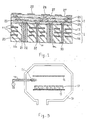
- the disclosed substrate includes an alumina ceramic substrate 1, wiring layers 2 made of an organic material, through-holes 12 penetrating the substrate 1, a power supply wiring layer 13 and a ground wiring layer 14. Since the layer 13 and 14, and the through-holes 12, each of which is connected to either the layer 13 or 14, are formed within the substrate 1 of a high relative dielectric constant, the voltage reduction over the layers 13 and 14 and across the through-holes 12 can be kept low. However, because the through-holes 12 are formed within the substrate 1 having the high relative dielectric constant, a signal-propagation delay time through some of the through-holes 12, which are used for signal transmission, increases inevitably.
- An object of the invention is, therefore, to provide a substrate free from the above-mentioned disadvantage in the prior art substrate.
- a substrate which comprises: a substrate section made of a ceramic material; a plurality of power supply wiring layers formed within said substrate section; a plurality of first and second through-holes penetrating said substrate section; first electrically conductive metal layers, each of which is formed on a wall surface of said substrate section to define each of said first through-holes and is connected electrically to at least one of said power supply wiring layers; coating layers of a fluoride resin dielectric, each of which is formed on a wall surface of said substrate section to define each of said second through-holes; second electrically conductive metal layers formed on said coating layers, respectively; and a circuit supplied with power via said first electrically conductive metal layers and with signals via said second electrically conductive metal layers.
- an embodiment of the invention comprises a power supply wiring layer section 1 and a signal wiring layer section 2.
- the section 1 comprises interlayer insulating layers 11 made by adding silicon oxide, calcium oxide, titanium oxide and magnesium oxide to aluminum oxide, which serves as a principal component of the layers 11, to achieve a relative dielectric constant of 10, and power supply wiring layers 12, 13 and 14 made of tungsten and interposed between the layers 11, respectively.
- Through-holes 20 of a diameter of 0.3 mm (milimeters) are bored at an interval of 1.5 mm in a grid pattern to penetrate through the substrate 1 from its upper surface to its lower surface.
- Wall surfaces 20a of the section 1 to define the respective through-holes 20 are coated with respective polytetrafluoroethylene film 21.
- Through-hole wirings 22 made of copper and having a diameter of 0.1 mm are formed within spaces surrounded by the films 21.
- the layers 12 and 13 are connected to power supply through-hole wirings 32 and 33, respectively.
- the wirings 32 and 33 are not surrounded with a polytetra fluoroethylene film.
- Pads 23 made of gold are provided on the upper surface of the section 1, and connected to the wirings 22, 32 and 33.
- the signal wiring layer section 2 comprising thin-film wiring layers 25 interposed between interlayer insulating layers 24 made of polyimide resin.
- the layers 25 are formed by gold-plating. Some of the layers 25 are connected to the wirings 22 via the pads 23.
- Each of via-holes 27 is bored through a corresponding one of the layers 24.
- Pads 28 made of copper are formed on the upper surface of the section 2 to be electrically connected to circuit elements such as large scale integrated circuits (not shown).
- the layers 25 are formed by gold-plating in the embodiment, they may be formed by copper-plating.
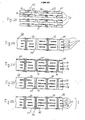
- a plurality of separate ceramic green sheets 50 are bored to form through-holes 20 for signals and through-holes 40 for power, and then are printed with a conductive paste containing tungsten, molybdenum or a palladium-silver alloy to form power supply pattern wirings 51 and through-hole wirings 52 and 53.
- these green sheets 50 are positionally adjusted each other, laminated, pressed, and fired.
- a laminated body 60 comprising a plurality of power supply wiring layers 12 to 14 laminated via interlayer insulating layers 11 made of ceramic is formed.
- the laminated body 60 is next placed in a plasma polymerization device 7 shown in FIG. 3.
- the device is depressurized to 5 x 10 ⁇ 3 Pa (Pascal), and is then placed in a atmosphere of a argon gas of 1 Pa.
- a tetrafluoroethylene gas 71 is being introduced from an inlet pipe 74 until the pressure inside the device 70 reaches 1 to 50 Pa.
- electric power of a high frequency of 13.56 megahertz is supplied between electrodes 72 and 73 to generate plasma. This forms polytetrafluoroethylene films on the upper surface of the laminated body 60 and the wall surfaces of the through-holes 20.
- the production rate of the polytetrafluoroethylene film becomes 1000 ⁇ (angstrom) per minute. At this rate, it takes three hours to form about 18 ⁇ (microns) of film. Then, the laminated body 60 is turned upside down to make the lower surface thereof face the electrode 72 so that a polytetrafluoroethylene film is formed under the same conditions as used for the upper surface. In this manner, as shown in FIG. 2C, both the upper and lower surfaces of the laminated body 60 and the wall surfaces of the through-holes 20 are coated with the polytetrafluoroethylene films 21, respectively.
- the upper and lower surfaces of the laminated body 60 are subsequently polished to remove the films 21 from the surfaces as shown in FIG. 2D.
- the films 21 on the wall surfaces of the through-holes 20 remain unremoved.
- the laminated body 60 is next placed in a cylindrical plasma etching device.
- the device is depressurized to a vacuum, fed with a reactive gas consisting of a mixture of 40 percent (%) by volume of oxygen and 60% by volume of nitrogen until the pressure inside the device becomes 50 Pa., and is supplied with a high frequency power of 13.56 megahertzs and 500 watts to perform plasma-etching for 5 minutes.
- a direct current magnetron sputtering device a chromium film of a thickness of 500 ⁇ and a palladium film of a thickness of 1000 ⁇ are sequentially formed on each of the upper and lower surfaces of the body 60 and the films 21 to form a two-film layer.
- the plasma etching is a pre-treatment of the direct current magnetron sputtering to activate the surfaces of the polytetrafluoroethylene films 21 so as to increase the adhesion to the two-film layers formed on the films, and is effective especially when conducted under a nitrogen gas including an oxygen gas of 40% by volume or more.
- the similar effect can be achieved by performing ion-milling with an argon gas mixed with an oxygen gas of 5 to 20% by volume, instead of the plasma etching. Since the ion-milling, however, is an anisotropic etching, some contrivances such as the rotating of the laminated body 60 should be made to uniformly process the through-holes as a whole.
- the two-film layers which have been formed by the spluttering device as mentioned above, may be formed by a vacuum deposition device, instead. Further, one film of the two-film layer may be made of titanium or copper instead of chromium, and the other film may be made of platinum, gold, or nickel instead of palladium.
- the surfaces of the two-film layers are coated with photosensitive resist of diazo group, only the resist within the through-holes 20 and on both ends of each of the through-hole wirings 32 and 33 is removed by exposure processing and development processing to form a resist pattern. Then, a copper film of a thickness of 1.5 ⁇ is formed by plating on each of the parts of the resist pattern from which the resist has been removed. The resist pattern is next removed by an organic solvent such as butanone, and the two-film layers are etched off by an ion-milling device. In this manner, as shown in FIG.
- the section 1 formed with the pads 23 each made of the palladium film, the chromium film and copper film and with the through-hole wirings 22 is completed.
- the copper plating has been used for the through-hole wirings 22 in the embodiment, the copper-plating may be replaced by gold-plating.
- the tetrafluoroethylene gas used to form the films 21 may be replaced by a chlorofluoroethylene gas to form films of polychlorofluoroethylene as the films 21 by a method similar to the above.
- the relative dielectric constant of 2.5 can be attained in the polychlorofluoroethylene films.
- the signal through-hole wirings 22 are coated with the fluoride resin films 21 having an extremely low relative dielectric constant, the signal propagation delay time over the through-hole wirings 22 can be minimized.
Landscapes
- Engineering & Computer Science (AREA)
- Microelectronics & Electronic Packaging (AREA)
- Production Of Multi-Layered Print Wiring Board (AREA)
Applications Claiming Priority (2)
| Application Number | Priority Date | Filing Date | Title |
|---|---|---|---|
| JP61209644A JPS6366993A (ja) | 1986-09-08 | 1986-09-08 | 多層配線基板 |
| JP209644/86 | 1986-09-08 |
Publications (3)
| Publication Number | Publication Date |
|---|---|
| EP0260857A2 true EP0260857A2 (fr) | 1988-03-23 |
| EP0260857A3 EP0260857A3 (en) | 1988-09-07 |
| EP0260857B1 EP0260857B1 (fr) | 1992-04-15 |
Family
ID=16576206
Family Applications (1)
| Application Number | Title | Priority Date | Filing Date |
|---|---|---|---|
| EP87307886A Expired - Lifetime EP0260857B1 (fr) | 1986-09-08 | 1987-09-07 | Substrat ayant des conducteurs électriques multicouches |
Country Status (4)
| Country | Link |
|---|---|
| US (1) | US4816323A (fr) |
| EP (1) | EP0260857B1 (fr) |
| JP (1) | JPS6366993A (fr) |
| DE (1) | DE3778261D1 (fr) |
Cited By (11)
| Publication number | Priority date | Publication date | Assignee | Title |
|---|---|---|---|---|
| GB2225670A (en) * | 1988-11-30 | 1990-06-06 | Hitachi Ltd | Carrier substrate for electrical circuit element |
| WO1991008588A1 (fr) * | 1989-12-01 | 1991-06-13 | Cray Research, Inc. | Procede et appareil d'interconnexions de puissance et densite elevees pour circuits integres |
| WO1991011025A1 (fr) * | 1990-01-16 | 1991-07-25 | A.S Micro Electronics | Procede de fabrication de systemes d'interconnexion miniaturises a impedances adaptees |
| EP0481472A1 (fr) * | 1990-10-17 | 1992-04-22 | Nec Corporation | Circuit imprimé multicouche et son procédé de fabrication |
| US5130229A (en) * | 1990-04-26 | 1992-07-14 | International Business Machines Corporation | Multi layer thin film wiring process featuring self-alignment of vias |
| US5219669A (en) * | 1990-04-26 | 1993-06-15 | International Business Machines Corporation | Layer thin film wiring process featuring self-alignment of vias |
| WO1993012539A1 (fr) * | 1991-12-19 | 1993-06-24 | Raychem Corporation | Bornes de transfert thermique pour substrats multipuces a haute densite et procede de formation |
| WO2000007233A1 (fr) * | 1998-07-31 | 2000-02-10 | Kulicke & Soffa Holdings, Inc. | Procede ameliore d'aplanissement de minces couches de film deposees sur une base commune de circuits |
| US6299053B1 (en) | 1998-08-19 | 2001-10-09 | Kulicke & Soffa Holdings, Inc. | Isolated flip chip or BGA to minimize interconnect stress due to thermal mismatch |
| US6317331B1 (en) | 1998-08-19 | 2001-11-13 | Kulicke & Soffa Holdings, Inc. | Wiring substrate with thermal insert |
| EP1473979A4 (fr) * | 2003-01-14 | 2006-04-26 | Matsushita Electric Industrial Co Ltd | Element haute frequence a structure stratifiee et procede permettant de produire cet element |
Families Citing this family (38)
| Publication number | Priority date | Publication date | Assignee | Title |
|---|---|---|---|---|
| US4931144A (en) * | 1987-07-31 | 1990-06-05 | Texas Instruments Incorporated | Self-aligned nonnested sloped via |
| JP3033972B2 (ja) * | 1989-06-15 | 2000-04-17 | 日本特殊陶業株式会社 | アルミナ多層配線基板及びその製造方法 |
| US5072075A (en) * | 1989-06-28 | 1991-12-10 | Digital Equipment Corporation | Double-sided hybrid high density circuit board and method of making same |
| JP3090453B2 (ja) * | 1989-07-10 | 2000-09-18 | 株式会社日立製作所 | 厚膜薄膜積層基板およびそれを用いた電子回路装置 |
| US5185502A (en) * | 1989-12-01 | 1993-02-09 | Cray Research, Inc. | High power, high density interconnect apparatus for integrated circuits |
| US5948533A (en) * | 1990-02-09 | 1999-09-07 | Ormet Corporation | Vertically interconnected electronic assemblies and compositions useful therefor |
| US5245751A (en) | 1990-04-27 | 1993-09-21 | Circuit Components, Incorporated | Array connector |
| US5071359A (en) | 1990-04-27 | 1991-12-10 | Rogers Corporation | Array connector |
| US5183972A (en) * | 1991-02-04 | 1993-02-02 | Microelectronics And Computer Technology Corporation | Copper/epoxy structures |
| US5227013A (en) * | 1991-07-25 | 1993-07-13 | Microelectronics And Computer Technology Corporation | Forming via holes in a multilevel substrate in a single step |
| US5440805A (en) * | 1992-03-09 | 1995-08-15 | Rogers Corporation | Method of manufacturing a multilayer circuit |
| US5287619A (en) * | 1992-03-09 | 1994-02-22 | Rogers Corporation | Method of manufacture multichip module substrate |
| US5521332A (en) * | 1992-08-31 | 1996-05-28 | Kyocera Corporation | High dielectric layer-containing alumina-based wiring substrate and package for semiconductor device |
| US5272600A (en) * | 1992-09-02 | 1993-12-21 | Microelectronics And Computer Technology Corporation | Electrical interconnect device with interwoven power and ground lines and capacitive vias |
| WO1994007348A1 (fr) * | 1992-09-24 | 1994-03-31 | Hughes Aircraft Company | Interconnexions entre couches dielectriques dans des structures/substrats tridimensionnels multicouches |
| US5868884A (en) * | 1994-03-25 | 1999-02-09 | Sumitomo Metal Industries, Ltd. | Method for producing ceramic dielectrics |
| US5712192A (en) * | 1994-04-26 | 1998-01-27 | International Business Machines Corporation | Process for connecting an electrical device to a circuit substrate |
| US6429113B1 (en) | 1994-04-26 | 2002-08-06 | International Business Machines Corporation | Method for connecting an electrical device to a circuit substrate |
| JPH08264956A (ja) * | 1995-03-23 | 1996-10-11 | Internatl Business Mach Corp <Ibm> | 電気的接続構造 |
| US5763059A (en) * | 1995-03-31 | 1998-06-09 | Kyocera Corporation | Circuit board |
| JP2833521B2 (ja) * | 1995-05-18 | 1998-12-09 | 日本電気株式会社 | 配線基板 |
| US5779836A (en) * | 1996-07-11 | 1998-07-14 | Advance Circuits Inc | Method for making a printed wiring board |
| US5763060A (en) * | 1996-07-11 | 1998-06-09 | Advance Circuits, Inc. | Printed wiring board |
| USRE40947E1 (en) | 1997-10-14 | 2009-10-27 | Ibiden Co., Ltd. | Multilayer printed wiring board and its manufacturing method, and resin composition for filling through-hole |
| US6085415A (en) * | 1998-07-27 | 2000-07-11 | Ormet Corporation | Methods to produce insulated conductive through-features in core materials for electric packaging |
| JP4442832B2 (ja) * | 1999-04-13 | 2010-03-31 | イビデン株式会社 | 多層プリント配線板 |
| CN1199536C (zh) * | 1999-10-26 | 2005-04-27 | 伊比登株式会社 | 多层印刷配线板及多层印刷配线板的制造方法 |
| JP3865989B2 (ja) * | 2000-01-13 | 2007-01-10 | 新光電気工業株式会社 | 多層配線基板、配線基板、多層配線基板の製造方法、配線基板の製造方法、及び半導体装置 |
| US6586682B2 (en) * | 2000-02-23 | 2003-07-01 | Kulicke & Soffa Holdings, Inc. | Printed wiring board with controlled line impedance |
| JP4459406B2 (ja) * | 2000-07-27 | 2010-04-28 | ソニーケミカル&インフォメーションデバイス株式会社 | フレキシブル配線板製造方法 |
| JP3527694B2 (ja) * | 2000-08-11 | 2004-05-17 | 新光電気工業株式会社 | 配線基板の製造方法 |
| JP4680410B2 (ja) * | 2001-04-24 | 2011-05-11 | 日本特殊陶業株式会社 | 配線基板 |
| JP2003101184A (ja) * | 2001-09-27 | 2003-04-04 | Kyocera Corp | セラミック回路基板およびその製造方法 |
| US6770822B2 (en) * | 2002-02-22 | 2004-08-03 | Bridgewave Communications, Inc. | High frequency device packages and methods |
| TW573444B (en) * | 2003-04-22 | 2004-01-21 | Ind Tech Res Inst | Substrate having organic and inorganic functional package |
| US7470863B2 (en) * | 2006-01-24 | 2008-12-30 | International Business Machines Corporation | Microelectronic device with mixed dielectric |
| US8581113B2 (en) | 2007-12-19 | 2013-11-12 | Bridgewave Communications, Inc. | Low cost high frequency device package and methods |
| JPWO2015151809A1 (ja) * | 2014-03-31 | 2017-04-13 | 株式会社村田製作所 | 積層配線基板およびこれを備えるプローブカード |
Family Cites Families (3)
| Publication number | Priority date | Publication date | Assignee | Title |
|---|---|---|---|---|
| US3698082A (en) * | 1966-04-25 | 1972-10-17 | Texas Instruments Inc | Complex circuit array method |
| CA1229155A (fr) * | 1983-03-29 | 1987-11-10 | Toshihiko Watari | Progiciel lsi a grande densite pour circuite logiques |
| JPS6156493A (ja) * | 1984-08-28 | 1986-03-22 | 日本電気株式会社 | 多層回路基板の電源配線構造 |
-
1986
- 1986-09-08 JP JP61209644A patent/JPS6366993A/ja active Pending
-
1987
- 1987-09-07 DE DE8787307886T patent/DE3778261D1/de not_active Expired - Lifetime
- 1987-09-07 EP EP87307886A patent/EP0260857B1/fr not_active Expired - Lifetime
- 1987-09-08 US US07/093,602 patent/US4816323A/en not_active Expired - Lifetime
Cited By (16)
| Publication number | Priority date | Publication date | Assignee | Title |
|---|---|---|---|---|
| GB2225670A (en) * | 1988-11-30 | 1990-06-06 | Hitachi Ltd | Carrier substrate for electrical circuit element |
| GB2225670B (en) * | 1988-11-30 | 1992-08-19 | Hitachi Ltd | Carrier substrate and method for preparing the same |
| WO1991008588A1 (fr) * | 1989-12-01 | 1991-06-13 | Cray Research, Inc. | Procede et appareil d'interconnexions de puissance et densite elevees pour circuits integres |
| US5127986A (en) * | 1989-12-01 | 1992-07-07 | Cray Research, Inc. | High power, high density interconnect method and apparatus for integrated circuits |
| WO1991011025A1 (fr) * | 1990-01-16 | 1991-07-25 | A.S Micro Electronics | Procede de fabrication de systemes d'interconnexion miniaturises a impedances adaptees |
| US5130229A (en) * | 1990-04-26 | 1992-07-14 | International Business Machines Corporation | Multi layer thin film wiring process featuring self-alignment of vias |
| US5219669A (en) * | 1990-04-26 | 1993-06-15 | International Business Machines Corporation | Layer thin film wiring process featuring self-alignment of vias |
| EP0481472A1 (fr) * | 1990-10-17 | 1992-04-22 | Nec Corporation | Circuit imprimé multicouche et son procédé de fabrication |
| WO1993012539A1 (fr) * | 1991-12-19 | 1993-06-24 | Raychem Corporation | Bornes de transfert thermique pour substrats multipuces a haute densite et procede de formation |
| WO2000007233A1 (fr) * | 1998-07-31 | 2000-02-10 | Kulicke & Soffa Holdings, Inc. | Procede ameliore d'aplanissement de minces couches de film deposees sur une base commune de circuits |
| US6165892A (en) * | 1998-07-31 | 2000-12-26 | Kulicke & Soffa Holdings, Inc. | Method of planarizing thin film layers deposited over a common circuit base |
| US6299053B1 (en) | 1998-08-19 | 2001-10-09 | Kulicke & Soffa Holdings, Inc. | Isolated flip chip or BGA to minimize interconnect stress due to thermal mismatch |
| US6317331B1 (en) | 1998-08-19 | 2001-11-13 | Kulicke & Soffa Holdings, Inc. | Wiring substrate with thermal insert |
| US6509529B2 (en) | 1998-08-19 | 2003-01-21 | Kulicke & Soffa Holdings, Inc. | Isolated flip chip of BGA to minimize interconnect stress due to thermal mismatch |
| EP1473979A4 (fr) * | 2003-01-14 | 2006-04-26 | Matsushita Electric Industrial Co Ltd | Element haute frequence a structure stratifiee et procede permettant de produire cet element |
| US7297878B2 (en) | 2003-01-14 | 2007-11-20 | Matsushita Electric Industrial Co., Ltd. | High frequency laminated component and its manufacturing method |
Also Published As
| Publication number | Publication date |
|---|---|
| JPS6366993A (ja) | 1988-03-25 |
| US4816323A (en) | 1989-03-28 |
| EP0260857B1 (fr) | 1992-04-15 |
| DE3778261D1 (de) | 1992-05-21 |
| EP0260857A3 (en) | 1988-09-07 |
Similar Documents
| Publication | Publication Date | Title |
|---|---|---|
| EP0260857A2 (fr) | Substrat ayant des conducteurs électriques multicouches | |
| JP3484306B2 (ja) | 薄膜コンデンサおよびその製造方法 | |
| EP1376686B1 (fr) | Méthode pour boucher des trous traversants dans un substrat de silicium | |
| EP0099544A1 (fr) | Procédé de fabrication de lignes conductrices et conducteurs de traversée sur substrats LSI | |
| US6423907B1 (en) | Components with releasable leads | |
| US3617373A (en) | Methods of making thin film patterns | |
| EP0905763A2 (fr) | Substrat à circuit multicouches et sa méthode de fabrication | |
| CN1123514A (zh) | 可层叠的电路板结构及制造方法 | |
| JPS639376B2 (fr) | ||
| US6323435B1 (en) | Low-impedance high-density deposited-on-laminate structures having reduced stress | |
| US5414224A (en) | Multilayer printed circuit board and method of manufacturing same | |
| EP1670297A2 (fr) | Plaquette à circuit imprimé et son procédé de fabrication | |
| US6495462B1 (en) | Components with releasable leads | |
| GB1591264A (en) | Electrical connection to semiconductor integrated circuits | |
| EP0982741B1 (fr) | Procédé de production d'une résistance à film mince sur un substrat céramique-polymère | |
| JP3360415B2 (ja) | 回路パターン形成方法 | |
| JPH055399B2 (fr) | ||
| JP3452677B2 (ja) | ファインパターン回路の形成方法 | |
| JP2565351B2 (ja) | 電子回路部品 | |
| JPH02303086A (ja) | プリント配線板の製造方法及びそれに用いるスパッタデポジション装置及び銅張積層板 | |
| WO1988005990A1 (fr) | Revetement de substrats avec des motifs metalliques epais formant des circuits | |
| JPH0240232B2 (fr) | ||
| Hanabusa et al. | High Density Multilayer Printed Wiring Boards Using UTC as the Surface Layer | |
| JPH0239589A (ja) | 回路基板の配線パターン形成法 | |
| EP1114439A2 (fr) | Procede de production de structures haute densite et basse impedance par depot sur stratifie |
Legal Events
| Date | Code | Title | Description |
|---|---|---|---|
| PUAI | Public reference made under article 153(3) epc to a published international application that has entered the european phase |
Free format text: ORIGINAL CODE: 0009012 |
|
| 17P | Request for examination filed |
Effective date: 19870922 |
|
| AK | Designated contracting states |
Kind code of ref document: A2 Designated state(s): DE FR GB |
|
| PUAL | Search report despatched |
Free format text: ORIGINAL CODE: 0009013 |
|
| AK | Designated contracting states |
Kind code of ref document: A3 Designated state(s): DE FR GB |
|
| 17Q | First examination report despatched |
Effective date: 19900730 |
|
| GRAA | (expected) grant |
Free format text: ORIGINAL CODE: 0009210 |
|
| AK | Designated contracting states |
Kind code of ref document: B1 Designated state(s): DE FR GB |
|
| REF | Corresponds to: |
Ref document number: 3778261 Country of ref document: DE Date of ref document: 19920521 |
|
| ET | Fr: translation filed | ||
| PLBE | No opposition filed within time limit |
Free format text: ORIGINAL CODE: 0009261 |
|
| STAA | Information on the status of an ep patent application or granted ep patent |
Free format text: STATUS: NO OPPOSITION FILED WITHIN TIME LIMIT |
|
| 26N | No opposition filed | ||
| REG | Reference to a national code |
Ref country code: GB Ref legal event code: IF02 |
|
| PGFP | Annual fee paid to national office [announced via postgrant information from national office to epo] |
Ref country code: GB Payment date: 20030903 Year of fee payment: 17 |
|
| PGFP | Annual fee paid to national office [announced via postgrant information from national office to epo] |
Ref country code: FR Payment date: 20030909 Year of fee payment: 17 |
|
| PGFP | Annual fee paid to national office [announced via postgrant information from national office to epo] |
Ref country code: DE Payment date: 20030918 Year of fee payment: 17 |
|
| PG25 | Lapsed in a contracting state [announced via postgrant information from national office to epo] |
Ref country code: GB Free format text: LAPSE BECAUSE OF NON-PAYMENT OF DUE FEES Effective date: 20040907 |
|
| PG25 | Lapsed in a contracting state [announced via postgrant information from national office to epo] |
Ref country code: DE Free format text: LAPSE BECAUSE OF NON-PAYMENT OF DUE FEES Effective date: 20050401 |
|
| GBPC | Gb: european patent ceased through non-payment of renewal fee |
Effective date: 20040907 |
|
| PG25 | Lapsed in a contracting state [announced via postgrant information from national office to epo] |
Ref country code: FR Free format text: LAPSE BECAUSE OF NON-PAYMENT OF DUE FEES Effective date: 20050531 |
|
| REG | Reference to a national code |
Ref country code: FR Ref legal event code: ST |