EP0261043A1 - Prüfgerät für elektronische Schaltungen - Google Patents
Prüfgerät für elektronische Schaltungen Download PDFInfo
- Publication number
- EP0261043A1 EP0261043A1 EP87420241A EP87420241A EP0261043A1 EP 0261043 A1 EP0261043 A1 EP 0261043A1 EP 87420241 A EP87420241 A EP 87420241A EP 87420241 A EP87420241 A EP 87420241A EP 0261043 A1 EP0261043 A1 EP 0261043A1
- Authority
- EP
- European Patent Office
- Prior art keywords
- circuit
- electronic
- tester
- circuits
- test
- Prior art date
- Legal status (The legal status is an assumption and is not a legal conclusion. Google has not performed a legal analysis and makes no representation as to the accuracy of the status listed.)
- Withdrawn
Links
- 238000012360 testing method Methods 0.000 claims abstract description 37
- 230000015654 memory Effects 0.000 claims abstract description 34
- 239000013598 vector Substances 0.000 claims abstract description 34
- 238000007493 shaping process Methods 0.000 abstract description 2
- 238000005259 measurement Methods 0.000 description 6
- 230000006870 function Effects 0.000 description 4
- 230000008901 benefit Effects 0.000 description 3
- 230000005540 biological transmission Effects 0.000 description 3
- 238000012795 verification Methods 0.000 description 3
- 238000004891 communication Methods 0.000 description 2
- 230000001934 delay Effects 0.000 description 2
- 230000000694 effects Effects 0.000 description 2
- 238000004519 manufacturing process Methods 0.000 description 2
- 230000004044 response Effects 0.000 description 2
- 230000006978 adaptation Effects 0.000 description 1
- 230000000712 assembly Effects 0.000 description 1
- 238000000429 assembly Methods 0.000 description 1
- 230000002457 bidirectional effect Effects 0.000 description 1
- 230000008859 change Effects 0.000 description 1
- 230000007547 defect Effects 0.000 description 1
- 230000007717 exclusion Effects 0.000 description 1
- 238000011990 functional testing Methods 0.000 description 1
- 230000004048 modification Effects 0.000 description 1
- 238000012986 modification Methods 0.000 description 1
- 230000008520 organization Effects 0.000 description 1
- 230000003071 parasitic effect Effects 0.000 description 1
- 239000011435 rock Substances 0.000 description 1
- 230000009897 systematic effect Effects 0.000 description 1
- 238000012546 transfer Methods 0.000 description 1
- 230000001131 transforming effect Effects 0.000 description 1
- 238000011282 treatment Methods 0.000 description 1
Images



Classifications
-
- G—PHYSICS
- G01—MEASURING; TESTING
- G01R—MEASURING ELECTRIC VARIABLES; MEASURING MAGNETIC VARIABLES
- G01R31/00—Arrangements for testing electric properties; Arrangements for locating electric faults; Arrangements for electrical testing characterised by what is being tested not provided for elsewhere
- G01R31/28—Testing of electronic circuits, e.g. by signal tracer
- G01R31/317—Testing of digital circuits
- G01R31/3181—Functional testing
- G01R31/319—Tester hardware, i.e. output processing circuits
- G01R31/31917—Stimuli generation or application of test patterns to the device under test [DUT]
- G01R31/31919—Storing and outputting test patterns
-
- G—PHYSICS
- G01—MEASURING; TESTING
- G01R—MEASURING ELECTRIC VARIABLES; MEASURING MAGNETIC VARIABLES
- G01R31/00—Arrangements for testing electric properties; Arrangements for locating electric faults; Arrangements for electrical testing characterised by what is being tested not provided for elsewhere
- G01R31/28—Testing of electronic circuits, e.g. by signal tracer
- G01R31/317—Testing of digital circuits
- G01R31/3181—Functional testing
- G01R31/319—Tester hardware, i.e. output processing circuits
- G01R31/31917—Stimuli generation or application of test patterns to the device under test [DUT]
- G01R31/31926—Routing signals to or from the device under test [DUT], e.g. switch matrix, pin multiplexing
Definitions
- the present invention relates to an electronic circuit tester.
- An integrated circuit for example, being generally intended to serve as a core for extremely complex assemblies, it is necessary initially to ensure that this circuit functions in all the possible configurations and in all the possible logical cases. Indeed, in use, a defect could only appear very late in a specific situation. Such a fault could then be catastrophic if, for example, this integrated circuit serves as the heart of a military, medical or industrial system.
- testers have been provided for verifying the proper functioning of electronic circuits
- integrated circuits often include structures which are not used in their normal operation but which are only intended to facilitate verifications of the proper functioning of the circuit.
- testers are devices used on the one hand by manufacturers of integrated circuits or complex electronic circuits, on the other hand by users who re-perform tests on each of the circuits they have acquired whereas, often, the manufacturer does in-depth verification only on a sample of the circuits he manufactures and validates a batch as soon as a certain percentage of circuits in the batch proves to be completely good.
- a tester has the following qualities: - high speed and precision of operation; indeed, many tests must be carried out on complex components and it is desirable that the elementary time occupied by each of the verifications be as short as possible; - simplicity of programming and flexibility of use; - great modularity, to allow the same tester to test different circuits while minimizing the changes to be made to the tester.
- test vectors are distributed bit by bit in the memories of the different channels and therefore difficult of access for the operator.
- a tester generally and successively performs three types of checks.
- a plausibility check that is to say a fairly coarse check in which one simply checks whether the various power supplies and the various input / output ports are not short-circuited or open circuit.
- a functional check which checks whether the circuit is working properly. For this, we send on one or more pins of the circuit to test suites of signals, called test vectors, formatted in duration and in amplitude and it is checked at the level of one or more other pins whether the signals received in response correspond well to the function expected from the circuit. At the functional control level, we also check whether the logic circuit has the speed that we expect. Typically, a basic functional test lasts around 100 ns and 4000 tests are carried out for a 256-pin integrated circuit.
- FIG. 1 An example of a conventional test machine is shown diagrammatically in FIG. 1. It is based on a large capacity central computer 10 connected on the one hand to external elements such as a terminal 11, a printer 12, and an access 13 intended to make the connection with other devices, for example a communication line to a host computer. On the other hand, the central unit 10 is connected to a bus 14 intended for transmitting and receiving data from the various elements of the tester.
- the circuit to be tested is connected to the tester via a not shown plug-in card, then a load card 15 whose input / output connections correspond to the number of pins of the element to be tested.
- Each of these connections is connected to a particular card, called an electronic pin, 16 of which only one is shown in FIG. 1 and which in fact constitutes a stack of cards, generally arranged geometrically in a ring.
- These cards 16 comprise, on the one hand, a bidirectional link to a memory of test vectors 17 and a personalized connection to a terminal of the load card 15 and, on the other hand, accesses to common circuits for supplying reference voltages, 19, and for supplying delay times, 19 ⁇ , and to the general bus 14.
- Each electronic pin 16 includes time shaping and leveling circuits to adjust the signals received from memory 17 to references supplied by circuits 19 and 19 ⁇ .
- the load card 15 includes adaptation impedances and switches for connecting the pins to be tested either to an electronic pin or to a measurement unit 18 which applies currents and measures voltages or vice versa.
- Each of the elements 15, 16, 17, 18, 19, 19 ⁇ must be programmed to ensure satisfactory operation and is connected to the common bus 14; each of these elements, or each of the sub-elements constituting each of these elements, is assigned a specific address making it possible to recognize the signals of the bus which are addressed to it and can conversely return on the bus characteristic signals which are detected by the computer 10.
- This description of a tester of the prior art is very schematic but is essentially intended to represent the overall architecture of a conventional tester based on a central computer and a common interconnection bus with modules which are connected in parallel on different addresses and which each provide one of the elementary functions of the tester.
- the operation of the modules 15, 16, 18, 19, 19 ⁇ and the operations to be carried out on these modules are inherently relatively slow, for example of the order of a millisecond or a tenth of a millisecond.
- the memory 17, which contains the test vectors which one wants to send to the circuit to be tested and those which one receives from it must be able to empty and fill up at a very rapid rate, usually of the order of ten nanoseconds. In fact, it must be possible to reach speeds corresponding to the maximum speeds for which the circuit to be tested has been designed in order to verify its operation at high frequency.
- the central computer 10 must manage the memory of test vectors 17 via the bus 14 extremely quickly.
- This memory 17 is a memory of very high capacity, for example several Mbytes. Consequently, in the testers of the prior art, various sophisticated means have been used to increase this management speed as much as possible, but this leads to relatively complex technical solutions because the bus 14 is extremely loaded due to its multiple connections to several modules and consequently its transmission speed is a priori limited.
- phase references are inevitably marred by systematic errors, different for the different pins, owing to the delays brought by the lengths of wires which cannot be negligible in such complex circuits.
- an object of the present invention is to provide a tester whose general architecture allows an increase in the speed of management of the memory of test vectors.
- Another object of the present invention is to provide a tester in which the connection between the circuit to be tested and the logic parts of the tester is improved to allow greater modularity.
- Another object of the present invention is to provide a tester making it possible to obtain well-determined time phase references.
- an electronic circuit tester comprising: a connection card for connection to each of the terminals of the circuit to be tested; n so-called electronic pin cards comprising means for formatting signals, each of which is connected to an input of the connection card; a single test vector memory module containing all the test vectors intended for and expected from the circuit, these vectors passing through said electronic pins; a central computer to manage the system and provide external links; wherein the management of the vector memory is performed concurrently by a memory management unit connected independently of the other modules of the tester to the central computer and an address processor operating asynchronously with respect to the central computer.
- this tester also comprises an analog measurement center, in which each electronic pin comprises on the same card: a programmable flip-flop circuit for synchronizing and imparting a predetermined delay to the test vectors transmitted by this electronic pin, a circuit providing said delay, leveling circuits programmable, and a multiplexing circuit for connecting the circuit to be tested either to the aforementioned circuits or to the analog measurement center.
- test vector memory is coupled to its own address processor and to its own memory management circuit allows very fast operation independently of the general bus of the central computer.
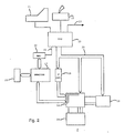
- FIG. 2 represents the general architecture of a tester according to the present invention presented as analogously as possible to the illustration of FIG. 1 in order to better highlight the differences between the architecture according to the present invention and the conventional architectures of prior art.
- FIG. 2 We find in FIG. 2 the central computer 10, the terminal 11, the printer 12 and the communication bus 13. However, the link between the central computer 10 and the various modules of the tester is different. Initially, in this figure, these modules have been represented in a similar manner to the case of FIG. 1 to facilitate comparison, but it will be seen below that the organization itself of these modules can be distinct. Thus, we find in FIG. 2 the memory of test vectors 17, the electronic pins 16 and the measurement unit 18. A common bus 20 is always used, but to perform the only “slow” operations, called configuration, at the exclusion of direct management of test vector memory.
- the computer 10 no longer communicates directly with the memory 17 but, via a link 21 such as a RS 232C serial link, with a particular memory management module 22 (commonly designated in the art by the acronym MMU after the Anglo-Saxon name Memory Management Unit).
- a specialized address processor 23 is provided, making it possible to carry out specific addressing sequences programmable in the memory. All these circuits are commercially available.
- MMU 22 we can choose a Motorola M6809 circuit and for the address processor a circuit from the AMD Company known as AM 2910 which enables very high addressing rates, which can exceed 10 MHz.
- This processor is associated with a variable frequency clock to allow, in some of these, to modify the cadence of the test sequences.
- the memory plane in which the test vectors are stored can therefore be shared between the MMU 22 which makes it possible to read and write conventionally in the memory for the purposes of observation or loading and the processor 23 which allows addressing of the memory for issue the test vectors at a rapid rate chosen according to the requirements of the test.
- the present invention provides a particular configuration and grouping of the various functions on the cards constituting the system.
- the block 19 ⁇ providing the time delay values for each pin no longer appears. In fact, it is incorporated into the electronic pin 16.
- the electronic pin is no longer associated with a charge card 15 but with a personalization card 24.
- This personalization card 24 no longer includes active programmable switches which are now reported in the electronic spindle, but only connection elements making it possible to electro-mechanically connect the pins of the circuit to be tested to the electronic spindle 16. Consequently, the measurement unit 18 is directly connected to the electronic pins.
- FIG. 3 shows functionally the association of the modules of the system.
- the central computer CPU 10 the bus 20 called configuration bus
- the link 21 with the MMU 22 the address processor 23
- the vector memory is organized into channels, each of which is connected to a particular electronic rock 16.
- Each electronic pin 16 comprises in particular: means 30 for ensuring synchronization and late adjustment, means 31 for ensuring level adjustment of the test vectors transmitted and received, and a multiplexer 36.
- the link between the vector memory of test 17 and the card 16 is done in one direction to transmit test vector signals (TEST) and, in the other direction, to receive in return analysis test vectors (ANAL) which are taken from the circuit to be checked and transmitted to the vector memory in order to be compared there with an expected response or to be stored there.
- TEST test vector signals
- ANL return analysis test vectors
- the delay adjustment circuits 30 essentially comprise a pair of flip-flops, 40, 41 on the TEST channel, and 42, 43 on the ANAL channel (FIG. 4).
- the first flip-flops 40, 42 ensure synchronization with the clock C1 of the address processor 23.
- the second flip-flops, 41, 43 receive an input from a delay circuit 19 ⁇ programmable under the effect of a command 32 from of the configuration bus 20. They make it possible to impose a given delay on the signals transmitted by the vector memory and those re-emitted by the electronic pin with respect to the clocking clock C1 of the address processor 23.
- the level adjustment circuit 31 includes impedance networks, conventionally produced using transistors, and receives its power supplies from the level reference module 19 programmable under the effect of a command 33 from the bus. configuration 20.
- This circuit 31 makes it possible to transform the logic signals coming from the test memory into voltage slots varying between high and low levels determined in accordance with the reference circuit of level 19. Conversely this circuit 31 comprises a return channel transforming into logic signals the voltages received from the spindle tested by comparison with reference values programmed by circuit 19.
- the multiplexer 36 makes it possible to switch the spindle of the circuit to be tested either to the circuits of the electronic spindle or to the measurement unit 18.
- each electronic pin 16 is directly coupled to the personalization card 24.
- the personalization card 24 according to the invention comprises a connector making it possible to connect to a circuit to be tested .
- the multiplexer 36 returns the outputs of the personalization card to the measurement center 18.
- These current and voltage measurement treatments being done in analog fashion, digital / analog and analog / digital converters should be provided in the measurement center 18 to communicate with the bus 20.
- FIG. 4 shows in a slightly more detailed form the main elements of the electronic pin 16, separating the directions of transmission.
- the synchronization and delay adjustment block 30 has been described previously.
- Block 31 comprises in the TEST direction an operational amplifier 44 fixing the high and low input levels V IH and V IL according to the values transmitted by block 19 which also provides high and low comparison levels V OH and V OL at comparators 45 and 46 analyzing the signals returned by the circuit to be tested.
- the mulitplexer 36 can be symbolized by two-way switches 47 and 48 connecting the personalization card to the other circuits of the electronic pin or to the central measurement unit 18.
- An additional advantage of the invention is that it makes it possible to manufacture a tester with a low operating cost for the user. This is in particular due to the fact that the multiplexer 36 is distributed over the electronic pins whereas it was conventionally provided on a charge card 15. The charge card was therefore an expensive card, these multiplexers incorporating numerous relays, and the user had to use a specific charge card for each family of circuits to be tested. According to the invention, it only has to change the personalization cards which do not include any expensive elements except connectors. In addition, due to their simplicity and their specialization, the personalization cards associated with the tester architecture according to the invention can be adapted to numerous circuits provided that they are mechanically compatible from the point of view of their pinout.
Landscapes
- Engineering & Computer Science (AREA)
- General Engineering & Computer Science (AREA)
- Physics & Mathematics (AREA)
- General Physics & Mathematics (AREA)
- Tests Of Electronic Circuits (AREA)
Applications Claiming Priority (2)
| Application Number | Priority Date | Filing Date | Title |
|---|---|---|---|
| FR8613304 | 1986-09-19 | ||
| FR8613304A FR2604260B1 (fr) | 1986-09-19 | 1986-09-19 | Testeur de circuits electroniques |
Publications (1)
| Publication Number | Publication Date |
|---|---|
| EP0261043A1 true EP0261043A1 (de) | 1988-03-23 |
Family
ID=9339209
Family Applications (1)
| Application Number | Title | Priority Date | Filing Date |
|---|---|---|---|
| EP87420241A Withdrawn EP0261043A1 (de) | 1986-09-19 | 1987-09-18 | Prüfgerät für elektronische Schaltungen |
Country Status (5)
| Country | Link |
|---|---|
| US (1) | US5111459A (de) |
| EP (1) | EP0261043A1 (de) |
| JP (1) | JPS63172436A (de) |
| CA (1) | CA1296062C (de) |
| FR (1) | FR2604260B1 (de) |
Cited By (1)
| Publication number | Priority date | Publication date | Assignee | Title |
|---|---|---|---|---|
| FR2684207A1 (fr) * | 1990-10-30 | 1993-05-28 | Teradyne Inc | Circuit interpolateur. |
Families Citing this family (8)
| Publication number | Priority date | Publication date | Assignee | Title |
|---|---|---|---|---|
| US5345393A (en) * | 1990-08-22 | 1994-09-06 | Matsushita Electric Industrial Co., Ltd. | Logic circuit generator |
| US5311448A (en) * | 1991-06-19 | 1994-05-10 | Compaq Computer Corporation | Programmable load board with programmable simulation of thermal dissipation characteristics |
| US5243274A (en) * | 1992-08-07 | 1993-09-07 | Westinghouse Electric Corp. | Asic tester |
| US5761214A (en) * | 1992-10-16 | 1998-06-02 | International Business Machines Corporation | Method for testing integrated circuit devices |
| KR100317727B1 (ko) * | 1993-01-19 | 2002-04-06 | 이데이 노부유끼 | 디바이스의 자동 측정방법 및 측정장치 |
| US5596587A (en) * | 1993-03-29 | 1997-01-21 | Teradyne, Inc. | Method and apparatus for preparing in-circuit test vectors |
| US5682392A (en) * | 1994-09-28 | 1997-10-28 | Teradyne, Inc. | Method and apparatus for the automatic generation of boundary scan description language files |
| US6275962B1 (en) * | 1998-10-23 | 2001-08-14 | Teradyne, Inc. | Remote test module for automatic test equipment |
Citations (1)
| Publication number | Priority date | Publication date | Assignee | Title |
|---|---|---|---|---|
| FR2543709A1 (fr) * | 1983-03-30 | 1984-10-05 | Centre Nat Rech Scient | Appareil programmable pour la generation de sequences numeriques en vue du test de circuits digitaux |
Family Cites Families (4)
| Publication number | Priority date | Publication date | Assignee | Title |
|---|---|---|---|---|
| US4092589A (en) * | 1977-03-23 | 1978-05-30 | Fairchild Camera And Instrument Corp. | High-speed testing circuit |
| US4517661A (en) * | 1981-07-16 | 1985-05-14 | International Business Machines Corporation | Programmable chip tester having plural pin unit buffers which each store sufficient test data for independent operations by each pin unit |
| US4517512A (en) * | 1982-05-24 | 1985-05-14 | Micro Component Technology, Inc. | Integrated circuit test apparatus test head |
| US4724378A (en) * | 1986-07-22 | 1988-02-09 | Tektronix, Inc. | Calibrated automatic test system |
-
1986
- 1986-09-19 FR FR8613304A patent/FR2604260B1/fr not_active Expired
-
1987
- 1987-09-16 CA CA000547008A patent/CA1296062C/en not_active Expired - Lifetime
- 1987-09-17 US US07/098,033 patent/US5111459A/en not_active Expired - Fee Related
- 1987-09-18 JP JP62234707A patent/JPS63172436A/ja active Pending
- 1987-09-18 EP EP87420241A patent/EP0261043A1/de not_active Withdrawn
Patent Citations (1)
| Publication number | Priority date | Publication date | Assignee | Title |
|---|---|---|---|---|
| FR2543709A1 (fr) * | 1983-03-30 | 1984-10-05 | Centre Nat Rech Scient | Appareil programmable pour la generation de sequences numeriques en vue du test de circuits digitaux |
Non-Patent Citations (3)
| Title |
|---|
| ELECTRONIC ENGINEERING, vol. 57, no. 707, novembre 1985, pages 153,156,157,159,161,162,165, Londres, GB; M. HAY: "A second generation performance tester" * |
| IBM TECHNICAL DISCLOSURE BULLETIN, vol. 25, no. 9, février 1983, pages 4872-4876, New York, US; T.V. LANDON et al.: "High speed hardware-based diagnostic system for high speed digital subsystems" * |
| WESCON TECHNICAL PAPERS, vol. 19, 16-19 septembre 1975, pages 27/2(1)-27/2(4), San Francisco, US; J.F. CAMPBELL, Jr.: "A new real-time funtion test generation system for complex LSI testing" * |
Cited By (1)
| Publication number | Priority date | Publication date | Assignee | Title |
|---|---|---|---|---|
| FR2684207A1 (fr) * | 1990-10-30 | 1993-05-28 | Teradyne Inc | Circuit interpolateur. |
Also Published As
| Publication number | Publication date |
|---|---|
| US5111459A (en) | 1992-05-05 |
| FR2604260A1 (fr) | 1988-03-25 |
| CA1296062C (en) | 1992-02-18 |
| JPS63172436A (ja) | 1988-07-16 |
| FR2604260B1 (fr) | 1988-12-30 |
Similar Documents
| Publication | Publication Date | Title |
|---|---|---|
| EP0407787B1 (de) | Testvorrichtung für gedruckte Schaltungskarten und ihre Anwendung für das Testen von gedruckten Schaltungskarten, in Form einer Multiplex-Demultiplexeinrichtung für numerische Signale | |
| FR2476851A1 (fr) | Procedes et appareils de controle automatique de circuits electriques | |
| EP0578540B1 (de) | Verfahren zur Prüfung der Funktionsfähigkeit einer ASIC-Schaltung und darauf bezogene ASIC-Schaltung | |
| EP1114377B1 (de) | Modulares datenerfassungssystem | |
| FR2604260A1 (fr) | Testeur de circuits electroniques | |
| FR2846491A1 (fr) | Architecture comprenant des cellules de remplacement pour reparer des erreurs de conception dans des circuits integres apres fabrication | |
| EP0504063B1 (de) | Sender-Empfänger für gleichzeitige, bidirektionelle Datenübertragung im Basisband | |
| EP0656591B1 (de) | Automatisches Testsystem mit integrierter Bussimulierung | |
| FR2733599A1 (fr) | Sonde de tension a concordance d'impedance | |
| FR2526957A1 (fr) | Memoire pour systeme de test | |
| EP0809255B1 (de) | Schieberegisterzelle | |
| EP1159628B1 (de) | Verfahren zur prüfung von integrierten schaltungen mit speicherelement-zugriff | |
| EP0729584B1 (de) | Vorrichtung zum elektrischen prüfen eines elements einer elektrichen verbindung | |
| EP0729672B1 (de) | Elektronische schalteranordnung | |
| EP0762285A1 (de) | Prüfbares elektronisches System | |
| CA2004924C (fr) | Systeme electronique a plusieurs unites amovibles | |
| FR2531791A1 (fr) | Circuit d'adressage pour equipement de test automatique | |
| EP0823088A1 (de) | Verfahren und vorrichtung zur parallelen automatischen prüfung von elektronischen schaltungen | |
| EP0453758B1 (de) | Mit integrierten Schaltungen versehene Prüfvorrichtung für eine gedruckte Schaltung und Anwendung dieser Vorrichtung zum Prüfen einer solchen gedruckten Schaltung | |
| EP0505541B1 (de) | Ausgabeverwaltungskreis für speicherprogrammierbare steuerung | |
| FR2730364A1 (fr) | Amplificateur programmable d'instrumentation | |
| EP0828163A1 (de) | Schaltung mit Einrichtung zur Strukturprüfung ohne besonderen speziell zugeordneten Prüfanschlussstift | |
| EP0594478B1 (de) | Anwendungsspezifische Integrierte Schaltung mit einem Mikroprozessor und Prüfmitteln | |
| EP0831408A1 (de) | Verfahren zur Entwicklung einer anwendungsspezifischen integrierten Schaltung (ASIC) und Emulator dafür | |
| EP3213214B1 (de) | Prüfstand und software für die prüfung einer elektrischen vorrichtung, insbesondere eines computers |
Legal Events
| Date | Code | Title | Description |
|---|---|---|---|
| PUAI | Public reference made under article 153(3) epc to a published international application that has entered the european phase |
Free format text: ORIGINAL CODE: 0009012 |
|
| AK | Designated contracting states |
Kind code of ref document: A1 Designated state(s): AT BE CH DE ES FR GB GR IT LI LU NL SE |
|
| 17P | Request for examination filed |
Effective date: 19880914 |
|
| 17Q | First examination report despatched |
Effective date: 19910531 |
|
| STAA | Information on the status of an ep patent application or granted ep patent |
Free format text: STATUS: THE APPLICATION IS DEEMED TO BE WITHDRAWN |
|
| 18D | Application deemed to be withdrawn |
Effective date: 19930401 |
|
| RIN1 | Information on inventor provided before grant (corrected) |
Inventor name: DEVIGNE, YVES |