EP0261689A2 - Geschwindigkeits-Regelsystem für einen Gleichstrommotor - Google Patents
Geschwindigkeits-Regelsystem für einen Gleichstrommotor Download PDFInfo
- Publication number
- EP0261689A2 EP0261689A2 EP87114032A EP87114032A EP0261689A2 EP 0261689 A2 EP0261689 A2 EP 0261689A2 EP 87114032 A EP87114032 A EP 87114032A EP 87114032 A EP87114032 A EP 87114032A EP 0261689 A2 EP0261689 A2 EP 0261689A2
- Authority
- EP
- European Patent Office
- Prior art keywords
- terminal
- transistor
- collector
- terminals
- resistor
- Prior art date
- Legal status (The legal status is an assumption and is not a legal conclusion. Google has not performed a legal analysis and makes no representation as to the accuracy of the status listed.)
- Granted
Links
Images




Classifications
-
- H—ELECTRICITY
- H02—GENERATION; CONVERSION OR DISTRIBUTION OF ELECTRIC POWER
- H02P—CONTROL OR REGULATION OF ELECTRIC MOTORS, ELECTRIC GENERATORS OR DYNAMO-ELECTRIC CONVERTERS; CONTROLLING TRANSFORMERS, REACTORS OR CHOKE COILS
- H02P7/00—Arrangements for regulating or controlling the speed or torque of electric DC motors
- H02P7/06—Arrangements for regulating or controlling the speed or torque of electric DC motors for regulating or controlling an individual DC dynamo-electric motor by varying field or armature current
- H02P7/18—Arrangements for regulating or controlling the speed or torque of electric DC motors for regulating or controlling an individual DC dynamo-electric motor by varying field or armature current by master control with auxiliary power
- H02P7/24—Arrangements for regulating or controlling the speed or torque of electric DC motors for regulating or controlling an individual DC dynamo-electric motor by varying field or armature current by master control with auxiliary power using discharge tubes or semiconductor devices
- H02P7/28—Arrangements for regulating or controlling the speed or torque of electric DC motors for regulating or controlling an individual DC dynamo-electric motor by varying field or armature current by master control with auxiliary power using discharge tubes or semiconductor devices using semiconductor devices
- H02P7/2805—Arrangements for regulating or controlling the speed or torque of electric DC motors for regulating or controlling an individual DC dynamo-electric motor by varying field or armature current by master control with auxiliary power using discharge tubes or semiconductor devices using semiconductor devices whereby the speed is regulated by measuring the motor speed and comparing it with a given physical value
-
- H—ELECTRICITY
- H02—GENERATION; CONVERSION OR DISTRIBUTION OF ELECTRIC POWER
- H02P—CONTROL OR REGULATION OF ELECTRIC MOTORS, ELECTRIC GENERATORS OR DYNAMO-ELECTRIC CONVERTERS; CONTROLLING TRANSFORMERS, REACTORS OR CHOKE COILS
- H02P7/00—Arrangements for regulating or controlling the speed or torque of electric DC motors
- H02P7/06—Arrangements for regulating or controlling the speed or torque of electric DC motors for regulating or controlling an individual DC dynamo-electric motor by varying field or armature current
- H02P7/18—Arrangements for regulating or controlling the speed or torque of electric DC motors for regulating or controlling an individual DC dynamo-electric motor by varying field or armature current by master control with auxiliary power
- H02P7/24—Arrangements for regulating or controlling the speed or torque of electric DC motors for regulating or controlling an individual DC dynamo-electric motor by varying field or armature current by master control with auxiliary power using discharge tubes or semiconductor devices
- H02P7/28—Arrangements for regulating or controlling the speed or torque of electric DC motors for regulating or controlling an individual DC dynamo-electric motor by varying field or armature current by master control with auxiliary power using discharge tubes or semiconductor devices using semiconductor devices
- H02P7/285—Arrangements for regulating or controlling the speed or torque of electric DC motors for regulating or controlling an individual DC dynamo-electric motor by varying field or armature current by master control with auxiliary power using discharge tubes or semiconductor devices using semiconductor devices controlling armature supply only
- H02P7/288—Arrangements for regulating or controlling the speed or torque of electric DC motors for regulating or controlling an individual DC dynamo-electric motor by varying field or armature current by master control with auxiliary power using discharge tubes or semiconductor devices using semiconductor devices controlling armature supply only using variable impedance
- H02P7/2885—Arrangements for regulating or controlling the speed or torque of electric DC motors for regulating or controlling an individual DC dynamo-electric motor by varying field or armature current by master control with auxiliary power using discharge tubes or semiconductor devices using semiconductor devices controlling armature supply only using variable impedance whereby the speed is regulated by measuring the motor speed and comparing it with a given physical value
-
- Y—GENERAL TAGGING OF NEW TECHNOLOGICAL DEVELOPMENTS; GENERAL TAGGING OF CROSS-SECTIONAL TECHNOLOGIES SPANNING OVER SEVERAL SECTIONS OF THE IPC; TECHNICAL SUBJECTS COVERED BY FORMER USPC CROSS-REFERENCE ART COLLECTIONS [XRACs] AND DIGESTS
- Y10—TECHNICAL SUBJECTS COVERED BY FORMER USPC
- Y10S—TECHNICAL SUBJECTS COVERED BY FORMER USPC CROSS-REFERENCE ART COLLECTIONS [XRACs] AND DIGESTS
- Y10S388/00—Electricity: motor control systems
- Y10S388/907—Specific control circuit element or device
- Y10S388/91—Operational/differential amplifier
-
- Y—GENERAL TAGGING OF NEW TECHNOLOGICAL DEVELOPMENTS; GENERAL TAGGING OF CROSS-SECTIONAL TECHNOLOGIES SPANNING OVER SEVERAL SECTIONS OF THE IPC; TECHNICAL SUBJECTS COVERED BY FORMER USPC CROSS-REFERENCE ART COLLECTIONS [XRACs] AND DIGESTS
- Y10—TECHNICAL SUBJECTS COVERED BY FORMER USPC
- Y10S—TECHNICAL SUBJECTS COVERED BY FORMER USPC CROSS-REFERENCE ART COLLECTIONS [XRACs] AND DIGESTS
- Y10S388/00—Electricity: motor control systems
- Y10S388/907—Specific control circuit element or device
- Y10S388/917—Thyristor or scr
Definitions
- the present invention relates to a motor control system, and more particularly to a circuit for controlling the rotational speed of a DC motor.
- the rotational speed of a DC motor is proportional to the counterelectromotive voltage. Accordingly, the principle for a speed control of a motor is to change a motor driving current in accordance with variation of a motor load and to counteract, by controlling a voltage between terminals of the motor, the variation of a voltage drop across an internal resistance of the motor caused by the change of the motor driving current. Thus,the counterelectromotive voltage of the motor becomes constant, and the rotational speed thereof is stabilized against the load variation.
- a speed control circuit of a DC motor is based upon the above-mentioned operating principle.
- the control circuit according to prior art has a drawback that the variation of a bias current due to the changes of a power source voltage and/or an operating temperature causes the counterelectromotive voltage of the motor to vary with the result of change in a rotational speed.
- an object of the present invention is to provide an improved motor speed control circuit.
- Another object of the present invention is to provide a control system for stabilizing a speed of a motor against not only variation in a motor load but also variations in a power source voltage and an operating temperature.
- a motor speed control system comprises a DC motor connected between a power source terminal and a first terminal, a resistor connected between the power source terminal and a second terminal, a resistance divider connected between the first and second terminals, a third terminal connected to a dividing point of the divider, a first transistor having a collector-emitter path connected between the first terminal and a reference terminal, a second transistor having a collector-emitter path connected between the second terminal and reference terminal, an error amplifier having first and second input terminals and an output terminal which is connected to the bases of the first and second transistors, means coupled between the first input terminal of the error amplifier and the first terminal for generating a reference voltage thereacross, and means for connecting the second input terminal of the error amplifier circuit to the third terminal.
- the reference voltage circuit is provided on the side of the first terminal and is thus disconnected from the second terminal. Accordingly, the counterelectromotive voltage of the motor is stabilized against the variation in a bias current flowing into the reference voltage generating means, so that the rotational speed of the motor is kept constant.
- a first transistor 6 for motor driving has its collector-emitter path connected between a first terminal 1 and a reference terminal 4 which is grounded, and a second transistor 7 has its collector-emitter path connected between a second terminal 2 and the reference terminal 4.
- the second terminal 2 is connected to one input termihal of an error amplifier 9 through a reference voltage circuit 8, and the other input terminal of the error amplifier circuit 9 to a third terminal 3.
- An output from the error amplifier circuit 9 is applied in common to the bases of the transistors 6 and 7.
- a DC motor 10 is connected between a power source 15 and the first terminal 1, and a resistor 13 between the power source 15 and second terminal 2.
- a resistor 11 is connected between the second and third terminals 2 and 3, and a resistor 12 between the first and third terminals 1 and 3. These resistors 11 and 12 constitute a voltage divider.
- a bias current I B is applied from an current source 16 to the reference voltage circuit 8 which hence generates a reference voltage thereacross.
- V M R M ⁇ I M + E a (1)
- R M the internal resistance of the DC motor 10
- I M a current flowing through the DC motor 10 (i.e., a motor driving current)
- E a a counterelectromotive voltage of the DC motor 10.
- V13 R3 x (I1 + I B + I7) (4) wherein R3 is the resistance value of the resistor 13.
- the collector current I7 of the transistor 7 is not supplied to the motor 10, the collector current I7 is designed to be 1/K (K positive value) of the collector current I6 of the transistor 6, as expressed by the following equation (6), for purpose of reducing power consumption.
- I6 K ⁇ I7 (6)
- the counterelectromotive voltage Ea is made constant against the variation in the motor current I M . Namely, even when a load of the motor 10 varies, the rotation speed thereof is kept constant.
- the change in the bias current I B can be made small, but it is amplified with K times, as is apparent from the equation (9). Since the collector current I7 of the transistor 7 is not used for driving the motor 10, the value of K is considerably increased to reduce the power consumption. Consequently, a large variation occurs in the counterelectromotive voltage Ea due to the change of the bias current I B , and the rotation speed of the motor cannot be kept constant.
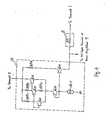
- a first embodiment of the present invention in which the same constituents as those shown in Fig. 1 are denoted by the same reference numerals to omit their further description.
- the reference voltage circuit 8 is connected between the first terminal 1 and the non-inverting input terminal (+) of the error or differential amplifier circuit 9, and a terminal 5 connected to the power source 15 is provided as a fifth terminal to disconnect the bias current source 16 from the second terminal 2.
- the bias current source 16 is connected between the terminal 5 and the reference voltage circuit 8. Accordingly, the bias current I B is supplied from the power source 15 without flowing through the resistor 13, and then flows into the transistor 6 through the reference voltage circuit 8.
- the equations (2) to (5) shown previously are rewritten to the following equations (10) to (13), respectively.
- a voltage V M between the terminals of the DC motor 10 is expressed by the following equation (14): >
- the counterelectromotive voltage Ea is represented as follows: This voltage Ea is constant irrespective of the variation of the motor current I M . Namely, a stabilized rotational speed of the motor against the load variation is obtained.
- the first member on the right side of the equation (15) does not contain the proportional constant K. Accordingly, even when the bias current I B varies slightly due to the variation of the voltage of the power source 15 and/or operating temperature, such slight variations are not amplified with K times. As a result, the rotation speed of the motor is also stabilized against the variations in the power source voltage and the operating temperature.
- Fig. 3 shows a detailed circuit construction of the embodiment of Fig. 1, wherein the transistors 6 and 7, the reference voltage circuit 8, the error amplifier 9 and the bias current source 16 are fabricated as a monolithic semiconductor integrated circuit device 100.
- the transistor 6 is formed of a plurality of unit transistors 6-1 to 6-N, and their collector-emitter paths are coupled in parallel, their bases being connected in common.
- the size of each of unit transistors is equal to the size of the transistor 7.
- the transistors 6-1 to 6-N and 7 have emitter resistors 6R-1 to 6R-N and 7R, respectively.
- the reference voltage circuit 8 consists of three NPN transistors Q5 to Q7 and three resistors 8R1 to 8R3 which are connected as shown in the drawing. This structure is known as a so-called “band gap regulator", which generates a reference voltage of about 1.2 V thereacross. This reference voltage does not change substantially irrespective of the variation in the voltage of the power source 15 and the operating temperature.
- the error amplifier 9 has two PNP transistors Q1 and Q2 connected in a differential form, the emitters of which are connected to a constant current source 9-1 through the respective emitter resistors 9R1 and 9R2.
- the base of the transistor Q1 is connected to the terminal 3 as an inverting input terminal (-), and the base of the transistor Q2 is connected as a non-inverting input terminal (+) to the node between the bias current source 16 and the reference voltage circuit 8.
- the collector of the transistor Q2 is connected to the reference terminal 4 through a diode D1 and a resistor 9R3, and further to the base of an NPN transistor Q3.
- the emitter of the transistor Q3 is connected to the reference terminal 4 through a resistor 9R4, and the collector thereof is connected to a constant current source 9-2 and the base of an NPN transistor Q4.
- the collector of the transistor Q4 is connected to the terminal 5, and the emitter thereof is connected to the reference terminal 4 through a resistor 9R5.
- the emitter of the transistor Q4 is led out as an output terminal of the error amplifier 9 and is connected in common to the bases of the transistors 7 and 6-1 to 6-N.
- the bias current source 16 has a band gap regulator consisting of transistors Q10 to Q12 and resistors 16R1 to 16R3, and the regulator is connected in series between the terminals 5 and 4 via a diode-connected transistor Q13 and a constant current source 16-1.
- transistor Q14 and a resistor 16R4 are further provided as shown in the drawing.
- the bias current I B takes a value of V B /R164 (R164 being a resistance value of the resistor 16R4), so that the change of the bias current I B with respect to the variation in the power source voltage and the operating temperature is reduced to an extremely low level.
- the transistor Q13 may be omitted.
- a diode is provided to be connected in series to the resistor 8R in the reference voltage circuit 8.
- Fig. 5 shows a second embodiment of the present invention, in which the same constituents as those shown in Fig. 2 are denoted by the same reference numerals to omit their explanation.
- an NPN transistor 17 is additionally provided.
- the collector-emitter path of this transistor 17 is inserted between the terminal 2 and the collector of the transistor 7, and the base of the transistor 17 is connected to the node between the reference voltage circuit 8 and the bias current source 14.
- the collector potential of the transistor 7 differs from the collector potential of the transistor 6 by a level that is equal to a voltage difference between the reference voltage V REF and a base-emitter forward voltage of the transistor 17.
- the collector-emitter voltage of the transistor 7 is rendered close to the collector-emitter voltage of the transistor 6, so that the transistor 7 is matched with the transistor 6 to obtain an accurate value of the proportional constant K.
- Fig. 6 shows a third embodiment of the present invention.
- the error amplifier 9 has a substantially identical construction as that shown in Fig. 3, and therefore includes the constant current source 9-1 between the terminal 5 and a node to which the emitters of the transistors Q1 and Q2 are connected in common through resistors 9R1 and 9R2.
- resistors 9R1 and 9R2 In order to expand the input dynamic range of the error amplifier 9, therefore, it is preferable to supply a lowered level of the voltage at the terminal 3 to the inverting input terminal (-) of the error amplifier 9.
- a transistor 60 and a constant current source 50 are provided as a level-shift circuit.
- the terminal 3 is connected via the base-emitter path of the transistor 60 to the inverting input terminal (-) of the error amplifier 9.
- the constant current source 50 maintains the voltage between the base and emitter of the transistor 60 at a constant level.
- the bias current source 16 has a band gap regulator consisting of transistors Q40 to Q42 and resistors R40 to R42 and connected in series between the terminals 4 and 5 via a constant current source 40.
- the band gap voltage V B is supplied to a series circuit consisting of the base-emitter path of a transistor Q43 and a resistor R43.
- the transistors Q44 and Q45 constitute a current mirror circuit in which the ratio of input current to output current is set to 1, and a collector current of the transistor Q43 is supplied as an input current for the current mirror circuit. Accordingly, the bias current I B from the bias current source 16 takes a value of (V B - V BE43 )/R43, wherein V BE43 is the voltage between the base and emitter of the transistor Q43.
- the reference voltage circuit 8 is formed of a single resistor R50, the resistance value of which is set to the same level as that of the resistor R43. Therefore, a voltage drop (V B - V BE43 ) occurs across the resistor R50.
- the voltage between the base and emitter of the transistor Q43 and that between the base and emitter of the transistor Q60 are substantially equal, the voltage between the terminals 3 and 1 is maintained at the level of the band gap voltage V B . This voltage is stabilized against the variations of the power source voltage and operating temperature. Moreover, the change of the bias current I B become very small.
- Fig. 7 shows an application of the present invention, which can change the rotation speed of the motor 10.
- a control circuit 300 can employ any one of the structures shown in Figs. 1, 3, 5 and 6. It is understood from the equation (15) that the counterelectromotive voltage Ea of the motor 10, i.e. the rotational speed thereof, can be switched from one value to another value by changing the resistance value of at least one of the resistors 11 and 12. In the circuit shown in Fig. 7, the resistance value of the resistor 12 is changed. To this end, a series circuit of a resistor 201 and the collector-emitter path of a transistor 200 is connected in parallel to the resistor 12. The base of the transistor 200 is connected to the power source 15 through a resistor 202 and a switch 203.
- the transistor 200 When the switch 203 is off, the transistor 200 is in a cut-off state, so that only the resistor 11 is connected between the terminals 1 and 3.
- the switch 203 When the switch 203 is turned on to energize the transistor 200, the resistor 201 is connected in parallel to the resistor 11, so that the resistance value between the terminals 1 and 3 becomes small. This causes the rotation speed of the motor to become low.
- the internal resistance R M of the motor 10 may become large as the rotational speed of the motor increases. If the resistance value of the resistor 13 as a torque control resistor is set constant nevertheless the internal resistance R M has become large, the variation of the rotational speed of the motor increases. Therefore, when the rotation speed of the motor is increased by changing the resistance value of at least one of the resistors 12 and 11, it is preferable to increase the resistance value of the resistor 13.
Landscapes
- Engineering & Computer Science (AREA)
- Power Engineering (AREA)
- Control Of Direct Current Motors (AREA)
Applications Claiming Priority (2)
| Application Number | Priority Date | Filing Date | Title |
|---|---|---|---|
| JP228595/86 | 1986-09-26 | ||
| JP22859586 | 1986-09-26 |
Publications (3)
| Publication Number | Publication Date |
|---|---|
| EP0261689A2 true EP0261689A2 (de) | 1988-03-30 |
| EP0261689A3 EP0261689A3 (en) | 1989-02-22 |
| EP0261689B1 EP0261689B1 (de) | 1993-03-17 |
Family
ID=16878817
Family Applications (1)
| Application Number | Title | Priority Date | Filing Date |
|---|---|---|---|
| EP87114032A Expired - Lifetime EP0261689B1 (de) | 1986-09-26 | 1987-09-25 | Geschwindigkeits-Regelsystem für einen Gleichstrommotor |
Country Status (5)
| Country | Link |
|---|---|
| US (1) | US4788478A (de) |
| EP (1) | EP0261689B1 (de) |
| JP (1) | JPS63186576A (de) |
| KR (1) | KR900007414B1 (de) |
| DE (1) | DE3784823T2 (de) |
Families Citing this family (5)
| Publication number | Priority date | Publication date | Assignee | Title |
|---|---|---|---|---|
| US5680037A (en) * | 1994-10-27 | 1997-10-21 | Sgs-Thomson Microelectronics, Inc. | High accuracy current mirror |
| US5610486A (en) * | 1995-02-28 | 1997-03-11 | Sgs-Thomson Microelectronics, Inc. | Current mirror circuit used in a coil driver circuit of a brushless DC motor |
| US6043623A (en) * | 1998-09-26 | 2000-03-28 | Bausch & Lomb Surgical, Inc. | Current compensation system for driving electric motor |
| FR2901927B1 (fr) * | 2006-06-01 | 2014-07-04 | Valeo Equip Electr Moteur | Machine tournante electrique triphasee |
| CN102248701A (zh) * | 2011-06-08 | 2011-11-23 | 天津市天锻压力机有限公司 | 移动回转压头框式液压机的变频器速度调节系统 |
Family Cites Families (6)
| Publication number | Priority date | Publication date | Assignee | Title |
|---|---|---|---|---|
| JPS5940000B2 (ja) * | 1977-11-14 | 1984-09-27 | 松下電器産業株式会社 | 直流モ−タの速度制御装置 |
| JPS5612886A (en) * | 1979-07-12 | 1981-02-07 | Fuji Electric Co Ltd | Speed control device for dc motor |
| US4350937A (en) * | 1979-08-04 | 1982-09-21 | Kabushiki Kaisha Sankyo Seiki Seisakusho | Motor speed control device for DC motor |
| FR2502419A1 (fr) * | 1981-03-20 | 1982-09-24 | Radiotechnique Compelec | Regulateur electronique de vitesse pour moteur a courant continu |
| JPS58165681A (ja) * | 1982-03-26 | 1983-09-30 | Sanyo Electric Co Ltd | 直流モ−タの速度制御回路 |
| US4547715A (en) * | 1984-07-09 | 1985-10-15 | Motorola, Inc. | Current control circuit |
-
1987
- 1987-09-17 JP JP62234306A patent/JPS63186576A/ja active Pending
- 1987-09-25 KR KR1019870010642A patent/KR900007414B1/ko not_active Expired
- 1987-09-25 DE DE8787114032T patent/DE3784823T2/de not_active Expired - Fee Related
- 1987-09-25 EP EP87114032A patent/EP0261689B1/de not_active Expired - Lifetime
- 1987-09-28 US US07/101,710 patent/US4788478A/en not_active Expired - Lifetime
Also Published As
| Publication number | Publication date |
|---|---|
| JPS63186576A (ja) | 1988-08-02 |
| DE3784823T2 (de) | 1993-09-09 |
| EP0261689B1 (de) | 1993-03-17 |
| DE3784823D1 (de) | 1993-04-22 |
| EP0261689A3 (en) | 1989-02-22 |
| KR880004632A (ko) | 1988-06-07 |
| US4788478A (en) | 1988-11-29 |
| KR900007414B1 (ko) | 1990-10-08 |
Similar Documents
| Publication | Publication Date | Title |
|---|---|---|
| US4475077A (en) | Current control circuit | |
| US4578633A (en) | Constant current source circuit | |
| JP2704245B2 (ja) | 基準電圧発生回路 | |
| US4325019A (en) | Current stabilizer | |
| EP0261689B1 (de) | Geschwindigkeits-Regelsystem für einen Gleichstrommotor | |
| JP2533201B2 (ja) | Am検波回路 | |
| JPH0365716A (ja) | 定電圧回路 | |
| US4498041A (en) | Constant current source circuit | |
| US5461343A (en) | Current mirror circuit | |
| US4560919A (en) | Constant-voltage circuit insensitive to source change | |
| JP2709033B2 (ja) | 定電圧発生回路 | |
| JPH0413692Y2 (de) | ||
| JPH0527139B2 (de) | ||
| JPS5986316A (ja) | 差動増幅器対の切替回路 | |
| JP3421430B2 (ja) | 電圧安定化回路 | |
| JPH0241276B2 (de) | ||
| KR0170357B1 (ko) | 온도 독립형 전류원 | |
| JPS62182819A (ja) | 電源回路 | |
| JP3226105B2 (ja) | 演算整流回路 | |
| JP2617123B2 (ja) | 安定化直流電源回路 | |
| JP3310033B2 (ja) | 定電圧回路 | |
| JPH0434567Y2 (de) | ||
| JP3403054B2 (ja) | 温度特性補正回路 | |
| JPH0415716A (ja) | 定電圧源回路 | |
| JP2650390B2 (ja) | 比較装置 |
Legal Events
| Date | Code | Title | Description |
|---|---|---|---|
| PUAI | Public reference made under article 153(3) epc to a published international application that has entered the european phase |
Free format text: ORIGINAL CODE: 0009012 |
|
| 17P | Request for examination filed |
Effective date: 19870925 |
|
| AK | Designated contracting states |
Kind code of ref document: A2 Designated state(s): DE FR GB |
|
| PUAL | Search report despatched |
Free format text: ORIGINAL CODE: 0009013 |
|
| AK | Designated contracting states |
Kind code of ref document: A3 Designated state(s): DE FR GB |
|
| 17Q | First examination report despatched |
Effective date: 19910201 |
|
| GRAA | (expected) grant |
Free format text: ORIGINAL CODE: 0009210 |
|
| AK | Designated contracting states |
Kind code of ref document: B1 Designated state(s): DE FR GB |
|
| REF | Corresponds to: |
Ref document number: 3784823 Country of ref document: DE Date of ref document: 19930422 |
|
| ET | Fr: translation filed | ||
| PLBE | No opposition filed within time limit |
Free format text: ORIGINAL CODE: 0009261 |
|
| STAA | Information on the status of an ep patent application or granted ep patent |
Free format text: STATUS: NO OPPOSITION FILED WITHIN TIME LIMIT |
|
| 26N | No opposition filed | ||
| PGFP | Annual fee paid to national office [announced via postgrant information from national office to epo] |
Ref country code: FR Payment date: 20010911 Year of fee payment: 15 |
|
| PGFP | Annual fee paid to national office [announced via postgrant information from national office to epo] |
Ref country code: GB Payment date: 20010926 Year of fee payment: 15 |
|
| PGFP | Annual fee paid to national office [announced via postgrant information from national office to epo] |
Ref country code: DE Payment date: 20011009 Year of fee payment: 15 |
|
| REG | Reference to a national code |
Ref country code: GB Ref legal event code: IF02 |
|
| PG25 | Lapsed in a contracting state [announced via postgrant information from national office to epo] |
Ref country code: GB Free format text: LAPSE BECAUSE OF NON-PAYMENT OF DUE FEES Effective date: 20020925 |
|
| PG25 | Lapsed in a contracting state [announced via postgrant information from national office to epo] |
Ref country code: DE Free format text: LAPSE BECAUSE OF NON-PAYMENT OF DUE FEES Effective date: 20030401 |
|
| GBPC | Gb: european patent ceased through non-payment of renewal fee |
Effective date: 20020925 |
|
| PG25 | Lapsed in a contracting state [announced via postgrant information from national office to epo] |
Ref country code: FR Free format text: LAPSE BECAUSE OF NON-PAYMENT OF DUE FEES Effective date: 20030603 |
|
| REG | Reference to a national code |
Ref country code: FR Ref legal event code: ST |