EP0261898A2 - Anzeigevorrichtung - Google Patents
Anzeigevorrichtung Download PDFInfo
- Publication number
- EP0261898A2 EP0261898A2 EP87308311A EP87308311A EP0261898A2 EP 0261898 A2 EP0261898 A2 EP 0261898A2 EP 87308311 A EP87308311 A EP 87308311A EP 87308311 A EP87308311 A EP 87308311A EP 0261898 A2 EP0261898 A2 EP 0261898A2
- Authority
- EP
- European Patent Office
- Prior art keywords
- pixel
- areas
- display device
- pixels
- scan
- Prior art date
- Legal status (The legal status is an assumption and is not a legal conclusion. Google has not performed a legal analysis and makes no representation as to the accuracy of the status listed.)
- Granted
Links
- 239000004973 liquid crystal related substance Substances 0.000 claims abstract description 5
- 238000000034 method Methods 0.000 claims description 9
- 210000002858 crystal cell Anatomy 0.000 claims description 3
- 238000001465 metallisation Methods 0.000 description 8
- 238000000059 patterning Methods 0.000 description 8
- 239000011521 glass Substances 0.000 description 5
- 239000002184 metal Substances 0.000 description 5
- 239000012769 display material Substances 0.000 description 3
- 239000004020 conductor Substances 0.000 description 2
- 238000013500 data storage Methods 0.000 description 2
- 239000005262 ferroelectric liquid crystals (FLCs) Substances 0.000 description 2
- 230000005540 biological transmission Effects 0.000 description 1
- 230000015572 biosynthetic process Effects 0.000 description 1
- 238000009413 insulation Methods 0.000 description 1
- 238000004519 manufacturing process Methods 0.000 description 1
- 239000000463 material Substances 0.000 description 1
- 230000035945 sensitivity Effects 0.000 description 1
Images


Classifications
-
- G—PHYSICS
- G09—EDUCATION; CRYPTOGRAPHY; DISPLAY; ADVERTISING; SEALS
- G09G—ARRANGEMENTS OR CIRCUITS FOR CONTROL OF INDICATING DEVICES USING STATIC MEANS TO PRESENT VARIABLE INFORMATION
- G09G3/00—Control arrangements or circuits, of interest only in connection with visual indicators other than cathode-ray tubes
- G09G3/20—Control arrangements or circuits, of interest only in connection with visual indicators other than cathode-ray tubes for presentation of an assembly of a number of characters, e.g. a page, by composing the assembly by combination of individual elements arranged in a matrix no fixed position being assigned to or needed to be assigned to the individual characters or partial characters
- G09G3/34—Control arrangements or circuits, of interest only in connection with visual indicators other than cathode-ray tubes for presentation of an assembly of a number of characters, e.g. a page, by composing the assembly by combination of individual elements arranged in a matrix no fixed position being assigned to or needed to be assigned to the individual characters or partial characters by control of light from an independent source
- G09G3/36—Control arrangements or circuits, of interest only in connection with visual indicators other than cathode-ray tubes for presentation of an assembly of a number of characters, e.g. a page, by composing the assembly by combination of individual elements arranged in a matrix no fixed position being assigned to or needed to be assigned to the individual characters or partial characters by control of light from an independent source using liquid crystals
- G09G3/3607—Control arrangements or circuits, of interest only in connection with visual indicators other than cathode-ray tubes for presentation of an assembly of a number of characters, e.g. a page, by composing the assembly by combination of individual elements arranged in a matrix no fixed position being assigned to or needed to be assigned to the individual characters or partial characters by control of light from an independent source using liquid crystals for displaying colours or for displaying grey scales with a specific pixel layout, e.g. using sub-pixels
-
- G—PHYSICS
- G02—OPTICS
- G02F—OPTICAL DEVICES OR ARRANGEMENTS FOR THE CONTROL OF LIGHT BY MODIFICATION OF THE OPTICAL PROPERTIES OF THE MEDIA OF THE ELEMENTS INVOLVED THEREIN; NON-LINEAR OPTICS; FREQUENCY-CHANGING OF LIGHT; OPTICAL LOGIC ELEMENTS; OPTICAL ANALOGUE/DIGITAL CONVERTERS
- G02F1/00—Devices or arrangements for the control of the intensity, colour, phase, polarisation or direction of light arriving from an independent light source, e.g. switching, gating or modulating; Non-linear optics
- G02F1/01—Devices or arrangements for the control of the intensity, colour, phase, polarisation or direction of light arriving from an independent light source, e.g. switching, gating or modulating; Non-linear optics for the control of the intensity, phase, polarisation or colour
- G02F1/13—Devices or arrangements for the control of the intensity, colour, phase, polarisation or direction of light arriving from an independent light source, e.g. switching, gating or modulating; Non-linear optics for the control of the intensity, phase, polarisation or colour based on liquid crystals, e.g. single liquid crystal display cells
- G02F1/133—Constructional arrangements; Operation of liquid crystal cells; Circuit arrangements
- G02F1/1333—Constructional arrangements; Manufacturing methods
- G02F1/1343—Electrodes
- G02F1/134309—Electrodes characterised by their geometrical arrangement
- G02F1/134336—Matrix
-
- G—PHYSICS
- G09—EDUCATION; CRYPTOGRAPHY; DISPLAY; ADVERTISING; SEALS
- G09F—DISPLAYING; ADVERTISING; SIGNS; LABELS OR NAME-PLATES; SEALS
- G09F9/00—Indicating arrangements for variable information in which the information is built-up on a support by selection or combination of individual elements
- G09F9/30—Indicating arrangements for variable information in which the information is built-up on a support by selection or combination of individual elements in which the desired character or characters are formed by combining individual elements
- G09F9/35—Indicating arrangements for variable information in which the information is built-up on a support by selection or combination of individual elements in which the desired character or characters are formed by combining individual elements being liquid crystals
-
- G—PHYSICS
- G02—OPTICS
- G02F—OPTICAL DEVICES OR ARRANGEMENTS FOR THE CONTROL OF LIGHT BY MODIFICATION OF THE OPTICAL PROPERTIES OF THE MEDIA OF THE ELEMENTS INVOLVED THEREIN; NON-LINEAR OPTICS; FREQUENCY-CHANGING OF LIGHT; OPTICAL LOGIC ELEMENTS; OPTICAL ANALOGUE/DIGITAL CONVERTERS
- G02F1/00—Devices or arrangements for the control of the intensity, colour, phase, polarisation or direction of light arriving from an independent light source, e.g. switching, gating or modulating; Non-linear optics
- G02F1/01—Devices or arrangements for the control of the intensity, colour, phase, polarisation or direction of light arriving from an independent light source, e.g. switching, gating or modulating; Non-linear optics for the control of the intensity, phase, polarisation or colour
- G02F1/13—Devices or arrangements for the control of the intensity, colour, phase, polarisation or direction of light arriving from an independent light source, e.g. switching, gating or modulating; Non-linear optics for the control of the intensity, phase, polarisation or colour based on liquid crystals, e.g. single liquid crystal display cells
- G02F1/133—Constructional arrangements; Operation of liquid crystal cells; Circuit arrangements
- G02F1/1333—Constructional arrangements; Manufacturing methods
- G02F1/1343—Electrodes
- G02F1/134309—Electrodes characterised by their geometrical arrangement
- G02F1/134345—Subdivided pixels, e.g. for grey scale or redundancy
-
- G—PHYSICS
- G09—EDUCATION; CRYPTOGRAPHY; DISPLAY; ADVERTISING; SEALS
- G09G—ARRANGEMENTS OR CIRCUITS FOR CONTROL OF INDICATING DEVICES USING STATIC MEANS TO PRESENT VARIABLE INFORMATION
- G09G3/00—Control arrangements or circuits, of interest only in connection with visual indicators other than cathode-ray tubes
- G09G3/20—Control arrangements or circuits, of interest only in connection with visual indicators other than cathode-ray tubes for presentation of an assembly of a number of characters, e.g. a page, by composing the assembly by combination of individual elements arranged in a matrix no fixed position being assigned to or needed to be assigned to the individual characters or partial characters
- G09G3/2007—Display of intermediate tones
- G09G3/2074—Display of intermediate tones using sub-pixels
Definitions
- the present invention relates to a display device and especially, but not solely, to a television receiver with a bistable display material e.g. ferroelectric liquid crystals.
- a bistable display material e.g. ferroelectric liquid crystals.
- U.S. Patent Specification No. 3845243 discloses a gas discharge display panel in which each display element is divided into several areas which can be individually energised. To display a grey scale the number of energised areas in each element is selected according to the required brightness value.
- British Patent Specification No.1390925 shows, in Figure 9, an electrode divided into several areas which can be selectively energised to control brightness.
- the present invention provides a display device comprising: a lattice of pixels to provide an image representing a picture signal; each pixel being divided into a plurality of areas each of which is individually settable to either of two states, only one said state producing a light output, the light outputs of the areas of a pixel not being the same; the areas of a pixel being arranged in substantially concentric manner.
- the human eye is very sensitive to small errors in apparent pixel position.
- the display device of the present invention overcomes any such positional error because the areas of a pixel may have essentially the same average position when viewed, so that different patterns of area driving in a pixel present a change of brightness, without any apparent positional change.
- the light outputs of the areas in a pixel have a binary relationship therebetween.
- a pixel has four distinct areas with light outputs in the ratio 8:4:2:1.
- the present invention also provides a display device comprising: a lattice of pixels to provide an image representing a picture-signal, each pixel being divided into a plurality of areas each individually settable to either of two states, only one said state producing a light output; means to effect two setting scans of the lattice for each received picture-signal; means to supply, in one said scan, to each of the pixels an amount of the relevant least-significant-bit information to effect setting for a first specified time period; and means to apply, in the other said scan, to each of the pixels an amount of the relevant most-significent-bit information to effect setting for a second specified time period.
- the display device has means to apply, in the first scan, the four least-significant-bits to set the pixels for substantially 1/17 of the time period for the picture, and means to apply, in the second scan, the four most-significantbits to set the pixels for substantially 16/17 of the time period for the picture.
- the present invention also provides a method of operating a display device, having a lattice of pixels to provide an image, each pixel being divided into a plurality of areas each individually settable to either of two states, only one said state producing a light output, the method comprising: effecting two setting scans of the lattice for each received picture; applying, in one said scan, to each of the pixels an amount of the relevant least-significent-bit information to set the pixel for a first specified time period; and applying, in the other said scan, to each of the pixels an amount of the relevant most-significant-bit information to set the pixel for a second specified time period.
- a display device embodying the present invention can be driven in any appropriate manner.
- such a display device may be driven in accordance with a technique utilising a number of drivers, each associated with a number of pixels, as described in a co-pending patent application belonging to the Applicant Company.
- a driving technique utilising time modulation as described in a co-pending patent application belonging to the Applicant Company.
- the binary relationship of the areas in a pixel of the present invention ensures that an amount of grey levels substantially greater than the number of areas can be achieved. Thus for four areas, sixteen grey levels are produced.
- each pixel is formed of a plurality of selectively-settable liquid crystal cells.
- the present invention is applicable to colour displays and to black-and-white displays.
- the present invention also embodies a display panel for use in a display device as herein defined. Furthermore, the present invention also embodies equipment for the generation, and/or transmission, and/or processing, and/or reception, of signals suited and/or designed for a display device as herein defined.
- the illustrated examples of the present invention involve the generation of a grey scale television image by the multiplexing of a bistable display material, namely ferroelectric liquid-crystal material, arranged to provide a lattice of pixels.
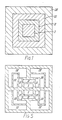
- Each pixel (see Figure 1) is formed of four areas I, II, III, IV which have light outputs in the ratio 1:2:4:8 respectively, thereby allowing a range of 16 grey levels which can be achieved by appropriate selection of areas.
- the concentric arrangement of the areas is significant. Since the human eye is very sensitive to small errors in apparent pixel position, it is important that each of the areas has the same average position, so that different bit patterns cause the pixel to change brightness only, without any apparent positional change.
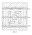
- the four areas are etched onto one piece of glass coated with ITO, and all four areas are addressed with one strobe line etched onto the opposite glass plate ( Figure 2).
- the active area of each pixel is reduced because of the area taken up by metal tracks bringing in data, resulting in some dimming of the displayed image.
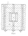
- Figure 3 to 5 illustrate a pixel metallisation pattern for a liquid crystal display device embodying the present invention.
- Figure 3 shows pixel boundary 1 and the row patterning formed by regions 2 of metal and regions 3 of ITO, with rows A1 and A2 relating to pixel areas II and IV and Row B relating to pixel areas I and III.
- Figure 4 shows the column patterning again formed by regions 2 of metal and regions 3 of ITO, with Columns C1 and C2 relating to pixel areas III and IV, and Column D relating to pixel areas I and II. When these row and column patterning are overlapped, the resulting formation of pixel is as shown in Figure 5.
- This arrangement is advantageous in that it avoids conductor crossovers on either display plate, thereby eliminating the possibility of electrical shorts otherwise caused by pinholes in crossover insulation.
- Figure 6 illustrates the arrangement of strobe and data lines on one plate 20 in respect of one pixel of a display while Figure 7 illustrates the arrangement of strobe and data lines on the other plate 21 in respect of the same pixel.
- three electrodes address three areas on each glass plate, one strobe line and two data.
- the pixel is still split into selectively settable areas in the ratio of 8:4:2:1 but any combinations of strobe and data lines can be used.
- one strobe 22 covers the areas corresponding to outputs with the ratio values 1 and 2 and is on side one of the glass plate 20 while the other strobe 23 covers the areas with output ratio values 4 and 8 of plate 21 (see Figures 6 and 7).
- the metal tracking is arranged so that tracks on one glass plate cover tracks on the other plate.
- the strobe pulses move in different directions on the screen, strobe 22 moving vertically while strobe 23 moves horizontally. This may make it necessary to process more data per frame but may reduce flicker in 25 Hz sequentially refreshed displays.
- the splitting of the strobe lines between the two plates is that both electrode and tracking patterns become of similar complexity, which is less (hence easier to manufacture, and with a higher degree of reliability) than the more complex plate in the type of arrangement of Figure 2.
- Plate 20 also has a line 24 for data bit 3 and a line 25 for data bit 4.
- Plate 21 has a line 26 for data bit 1 and lines 27, 28 for data bit 2.
- the four least significant bits of the image are input to the pixel as the video signal arrives, and the four most significant bits are input to the same pixel 1/17 of the frame time later.
- two display lines need to be addressed every video line.
- the most significant bits are displayed for 16/17 of the time, and the least significant for 1/17 of the time. Flicker will be minimal, and the data storage required is 1/34 of a frame store, being half the number of bits for 1/17 of the time.
- Such an operation enables the display device to achieve a range of 256 grey levels.
- the operation may be extended to 12 bits by inputting the 4 least significant bits as the video signal arrives, the middle 4 bits 1/273 of a frame later, and the most significant bits 16/273 of a frame after that.
- the storage required for a 12 bit display is not significantly greater than that for an 8 bit display, but the time in which to address a pixel is less, as three display lines rather than two need to be addressed in one video line time.
- the display device of the invention acts as an accurate D/A converter, converting the input digital data into visible light intensity. Therefore, to avoid contouring effects, the normal requirements of a D/A converter as regards bit accuracy and stability etc. must be met. For example, the time delay between displaying the sets of 4 bits determines the relative brightness, and should be accordingly accurate; this can be readily achieved.
- the bistable display material may not switch completely between states immediately, but may take some time to settle; such an effect could be compensated by adjusting the exposure time of the least significant bits, or by altering the stored bit pattern.
- the active transparent area of pixel area on one plate is arranged to be larger than that on the other plate, such that a small misalignment between the two plates does not alter the visible pixel area.
- the display device of the invention allows the maximum time for multiplexing bistable pixels, while still allowing the grey scale display to be updated at video rates. Also, it minimises display flicker, and minimises the amount of data storage required. Because of the maximum action of the time of addressing each row of the display, the pixels are updated in sequence and are continuously visible. If a colour display is required, separate red, green, and blue pixels must be used rather than field sequential colour with monochrome pixels.
Landscapes
- Physics & Mathematics (AREA)
- Crystallography & Structural Chemistry (AREA)
- Engineering & Computer Science (AREA)
- Chemical & Material Sciences (AREA)
- General Physics & Mathematics (AREA)
- Nonlinear Science (AREA)
- Theoretical Computer Science (AREA)
- Optics & Photonics (AREA)
- Geometry (AREA)
- Computer Hardware Design (AREA)
- Mathematical Physics (AREA)
- Liquid Crystal (AREA)
- Control Of Indicators Other Than Cathode Ray Tubes (AREA)
- Liquid Crystal Display Device Control (AREA)
- Devices For Indicating Variable Information By Combining Individual Elements (AREA)
- Control Of El Displays (AREA)
- Measuring Pulse, Heart Rate, Blood Pressure Or Blood Flow (AREA)
- Diaphragms For Electromechanical Transducers (AREA)
- Vehicle Body Suspensions (AREA)
- Control Of Gas Discharge Display Tubes (AREA)
- Transforming Electric Information Into Light Information (AREA)
Priority Applications (1)
| Application Number | Priority Date | Filing Date | Title |
|---|---|---|---|
| AT87308311T ATE88020T1 (de) | 1986-09-20 | 1987-09-18 | Anzeigevorrichtung. |
Applications Claiming Priority (2)
| Application Number | Priority Date | Filing Date | Title |
|---|---|---|---|
| GB8622715 | 1986-09-20 | ||
| GB868622715A GB8622715D0 (en) | 1986-09-20 | 1986-09-20 | Display device |
Publications (3)
| Publication Number | Publication Date |
|---|---|
| EP0261898A2 true EP0261898A2 (de) | 1988-03-30 |
| EP0261898A3 EP0261898A3 (en) | 1990-05-30 |
| EP0261898B1 EP0261898B1 (de) | 1993-04-07 |
Family
ID=10604539
Family Applications (1)
| Application Number | Title | Priority Date | Filing Date |
|---|---|---|---|
| EP87308311A Revoked EP0261898B1 (de) | 1986-09-20 | 1987-09-18 | Anzeigevorrichtung |
Country Status (7)
| Country | Link |
|---|---|
| US (1) | US5124695A (de) |
| EP (1) | EP0261898B1 (de) |
| JP (1) | JPH0664421B2 (de) |
| AT (1) | ATE88020T1 (de) |
| DE (1) | DE3785282T2 (de) |
| ES (1) | ES2039448T3 (de) |
| GB (1) | GB8622715D0 (de) |
Cited By (10)
| Publication number | Priority date | Publication date | Assignee | Title |
|---|---|---|---|---|
| EP0361981A3 (en) * | 1988-09-30 | 1990-08-16 | Sharp Kabushiki Kaisha | Liquid crystal display device for display with gray levels |
| EP0600537A1 (de) * | 1992-11-30 | 1994-06-08 | Koninklijke Philips Electronics N.V. | Anzeigevorrichtung |
| EP0703562A2 (de) | 1994-09-26 | 1996-03-27 | Canon Kabushiki Kaisha | Verfahren und Einrichtung zum Steuern eines Anzeigegeräts |
| EP0788014A2 (de) | 1996-02-01 | 1997-08-06 | Canon Kabushiki Kaisha | Anzeigevorrichtung für Graustufenanzeige |
| EP0778440A3 (de) * | 1995-12-05 | 1998-08-26 | Matsushita Electric Industrial Co., Ltd. | Rückleuchtenvorrichtung und Farbanzeiger |
| US5899550A (en) * | 1996-08-26 | 1999-05-04 | Canon Kabushiki Kaisha | Display device having different arrangements of larger and smaller sub-color pixels |
| US5963190A (en) * | 1994-09-26 | 1999-10-05 | Canon Kabushiki Kaisha | Driving method for display device and display apparatus |
| EP1024473A3 (de) * | 1999-01-29 | 2000-11-08 | Seiko Epson Corporation | Elektrolumineszensanzeige mit aktiver Matrix und Graustufensteuerung |
| WO2005059875A3 (en) * | 2003-12-16 | 2006-03-02 | Koninkl Philips Electronics Nv | A display panel comprising a plurality of pixels and a display device |
| EP1450408A3 (de) * | 2003-02-20 | 2010-05-05 | Barco N.V. | Anzeigenelementarray für emittierende Anzeigevorrichtung mit adressierbaren Pixeln |
Families Citing this family (47)
| Publication number | Priority date | Publication date | Assignee | Title |
|---|---|---|---|---|
| US5264835A (en) * | 1988-07-21 | 1993-11-23 | Proxima Corporation | Enhanced color display system and method of using same |
| NL9000942A (nl) * | 1990-04-20 | 1991-11-18 | Philips Nv | Weergeefinrichting. |
| US5225919A (en) * | 1990-06-21 | 1993-07-06 | Matsushita Electric Industrial Co., Ltd. | Optical modulation element including subelectrodes |
| US5245450A (en) * | 1990-07-23 | 1993-09-14 | Hosiden Corporation | Liquid crystal display device with control capacitors for gray-scale |
| TW228633B (de) * | 1991-01-17 | 1994-08-21 | Semiconductor Energy Res Co Ltd | |
| EP0584963B1 (de) * | 1992-07-30 | 2001-10-04 | Canon Kabushiki Kaisha | Flüssigkristall-Anzeigevorrichtung |
| US6714212B1 (en) | 1993-10-05 | 2004-03-30 | Canon Kabushiki Kaisha | Display apparatus |
| KR100259783B1 (ko) * | 1994-03-11 | 2000-06-15 | 미다라이 후지오 | 다수의 컬러 개별 레벨 디스플레이를 위한 디스플레이 픽셀 밸런싱 |
| AU683131B2 (en) * | 1994-03-11 | 1997-10-30 | Canon Kabushiki Kaisha | A luminance weighted discrete level display |
| AUPM440994A0 (en) * | 1994-03-11 | 1994-04-14 | Canon Information Systems Research Australia Pty Ltd | A luminance weighted discrete level display |
| JP3191081B2 (ja) * | 1994-03-11 | 2001-07-23 | キヤノン株式会社 | ディスプレイ装置 |
| AU679609B2 (en) * | 1994-03-11 | 1997-07-03 | Canon Kabushiki Kaisha | A manufacturing method for high quality discrete level displays |
| AU679831B2 (en) * | 1994-03-11 | 1997-07-10 | Canon Kabushiki Kaisha | Contrast enhancement for a flat panel display device |
| AUPM440494A0 (en) * | 1994-03-11 | 1994-04-14 | Canon Information Systems Research Australia Pty Ltd | Intermingling subpixels in discrete level displays |
| AU681234B2 (en) * | 1994-03-11 | 1997-08-21 | Canon Kabushiki Kaisha | Display pixel balancing for a multi colour discrete level display |
| AU683710B2 (en) * | 1994-03-11 | 1997-11-20 | Canon Kabushiki Kaisha | Intermingling subpixels in discrete level displays |
| TW295652B (de) * | 1994-10-24 | 1997-01-11 | Handotai Energy Kenkyusho Kk | |
| JP3520382B2 (ja) * | 1995-02-01 | 2004-04-19 | セイコーエプソン株式会社 | 液晶表示装置 |
| US5920299A (en) * | 1995-12-28 | 1999-07-06 | Canon Kabushiki Kaisha | Color display panel and apparatus |
| US6014121A (en) * | 1995-12-28 | 2000-01-11 | Canon Kabushiki Kaisha | Display panel and apparatus capable of resolution conversion |
| AUPN958996A0 (en) * | 1996-05-01 | 1996-05-23 | Canon Information Systems Research Australia Pty Ltd | Seamless parallel neighbourhood-process halftoning |
| US6489940B1 (en) * | 1998-07-31 | 2002-12-03 | Canon Kabushiki Kaisha | Display device driver IC |
| US6642914B1 (en) * | 2000-04-13 | 2003-11-04 | Hewlett-Packard Development Company, L.P. | Liquid crystal display (LCD) having improved isocontrast performance and method for producing same |
| JP2001350430A (ja) * | 2000-06-09 | 2001-12-21 | Mitsubishi Electric Corp | 表示装置 |
| JP2002333870A (ja) * | 2000-10-31 | 2002-11-22 | Matsushita Electric Ind Co Ltd | 液晶表示装置、el表示装置及びその駆動方法、並びに副画素の表示パターン評価方法 |
| US7023457B2 (en) * | 2001-03-13 | 2006-04-04 | Intel Corporation | System and method for intensity control of a pixel |
| US6961040B2 (en) | 2001-04-19 | 2005-11-01 | Eizo Nanao Corporation | Two-dimensional monochrome bit face display |
| US6956553B2 (en) * | 2001-04-27 | 2005-10-18 | Sanyo Electric Co., Ltd. | Active matrix display device |
| US7081870B2 (en) * | 2001-05-09 | 2006-07-25 | Hewlett-Packard Development Company, L.P. | Wearable display and method of displaying images using a wearable display |
| US7079164B2 (en) * | 2001-08-03 | 2006-07-18 | Lg.Philips Lcd Co., Ltd. | Method and apparatus for driving liquid crystal display panel |
| GB0119707D0 (en) * | 2001-08-13 | 2001-10-03 | Liquid Display Ltd | Display |
| JP4342200B2 (ja) | 2002-06-06 | 2009-10-14 | シャープ株式会社 | 液晶表示装置 |
| US20040080479A1 (en) * | 2002-10-22 | 2004-04-29 | Credelle Thomas Lioyd | Sub-pixel arrangements for striped displays and methods and systems for sub-pixel rendering same |
| US7397455B2 (en) * | 2003-06-06 | 2008-07-08 | Samsung Electronics Co., Ltd. | Liquid crystal display backplane layouts and addressing for non-standard subpixel arrangements |
| US7791679B2 (en) | 2003-06-06 | 2010-09-07 | Samsung Electronics Co., Ltd. | Alternative thin film transistors for liquid crystal displays |
| US20070195042A1 (en) * | 2004-04-13 | 2007-08-23 | Koninklijke Philips Electronics, N.V. | Liquid Crystal Display Device |
| JP4208763B2 (ja) * | 2004-04-28 | 2009-01-14 | キヤノン株式会社 | カラー表示素子及びカラー液晶表示素子 |
| JP5090620B2 (ja) * | 2004-12-27 | 2012-12-05 | シャープ株式会社 | 液晶表示装置 |
| CN101373580B (zh) * | 2005-03-29 | 2011-02-02 | 精工爱普生株式会社 | 电泳显示装置的驱动方法 |
| JP4419944B2 (ja) * | 2005-03-29 | 2010-02-24 | セイコーエプソン株式会社 | 電気泳動表示装置及びその駆動方法 |
| WO2007091365A1 (ja) * | 2006-02-06 | 2007-08-16 | Sharp Kabushiki Kaisha | 表示装置、アクティブマトリクス基板、液晶表示装置、テレビジョン受像機 |
| US8144115B2 (en) | 2006-03-17 | 2012-03-27 | Konicek Jeffrey C | Flat panel display screen operable for touch position determination system and methods |
| US7859526B2 (en) * | 2006-05-01 | 2010-12-28 | Konicek Jeffrey C | Active matrix emissive display and optical scanner system, methods and applications |
| JP5961060B2 (ja) * | 2012-07-18 | 2016-08-02 | 株式会社ジャパンディスプレイ | 液晶表示装置 |
| JP5827970B2 (ja) * | 2013-03-25 | 2015-12-02 | 株式会社ジャパンディスプレイ | 表示装置及び電子機器 |
| CN104465714B (zh) * | 2014-12-30 | 2017-04-26 | 京东方科技集团股份有限公司 | 一种像素结构及其显示方法、显示装置 |
| US11145251B2 (en) * | 2018-10-23 | 2021-10-12 | Innolux Corporation | Display device |
Family Cites Families (25)
| Publication number | Priority date | Publication date | Assignee | Title |
|---|---|---|---|---|
| US3647958A (en) * | 1970-08-31 | 1972-03-07 | Zenith Radio Corp | Flat-panel image display with plural display devices at each image point |
| GB1390925A (en) * | 1971-09-01 | 1975-04-16 | Rank Organisation Ltd | Optical display device |
| JPS5238693B2 (de) * | 1971-12-30 | 1977-09-30 | ||
| US3845243A (en) * | 1973-02-28 | 1974-10-29 | Owens Illinois Inc | System for producing a gray scale with a gaseous display and storage panel using multiple discharge elements |
| US3997719A (en) * | 1975-03-19 | 1976-12-14 | Bell Telephone Laboratories, Incorporated | Bi-level display systems |
| NL7903515A (nl) * | 1979-05-04 | 1980-11-06 | Philips Nv | Modulatorschakeling voor een matrixweergeefinrichting. |
| US4328492A (en) * | 1979-09-06 | 1982-05-04 | Tadeusz Bobak | Automatic display system and process |
| JPS5688193A (en) * | 1979-12-19 | 1981-07-17 | Citizen Watch Co Ltd | Display unit |
| FR2493012B1 (fr) * | 1980-10-27 | 1987-04-17 | Commissariat Energie Atomique | Procede de commande d'une caracteristique optique d'un materiau |
| US4661809A (en) * | 1982-05-05 | 1987-04-28 | Litton Systems, Inc. | Magneto-optic chip with gray-scale capability |
| US4559535A (en) * | 1982-07-12 | 1985-12-17 | Sigmatron Nova, Inc. | System for displaying information with multiple shades of a color on a thin-film EL matrix display panel |
| EP0109160A3 (de) * | 1982-10-14 | 1986-04-09 | The Secretary of State for Defence in Her Britannic Majesty's Government of the United Kingdom of Great Britain and | Elektronische Anzeigeeinrichtung |
| JPS59155832A (ja) * | 1983-02-24 | 1984-09-05 | Seiko Epson Corp | 中間調表示用液晶パネル |
| CH666560A5 (de) * | 1983-03-01 | 1988-07-29 | Tadeusz Bobak | Anzeigevorrichtung. |
| US4531160A (en) * | 1983-05-03 | 1985-07-23 | Itek Corporation | Display processor system and method |
| EP0149261B1 (de) * | 1984-01-13 | 1988-12-07 | Koninklijke Philips Electronics N.V. | Matrixsteuerschaltung für eine Speicher-Anzeigevorrichtung |
| GB8402654D0 (en) * | 1984-02-01 | 1984-03-07 | Secr Defence | Flatpanel display |
| JPS60256196A (ja) * | 1984-06-01 | 1985-12-17 | 株式会社日立製作所 | メモリパネル駆動方式 |
| JPS6142591U (ja) * | 1984-08-24 | 1986-03-19 | ソニー株式会社 | 液晶表示装置 |
| US4712877A (en) * | 1985-01-18 | 1987-12-15 | Canon Kabushiki Kaisha | Ferroelectric display panel of varying thickness and driving method therefor |
| FR2580110B1 (de) * | 1985-04-04 | 1987-05-29 | Commissariat Energie Atomique | |
| JPS6227716A (ja) * | 1985-07-29 | 1987-02-05 | Fuji Photo Film Co Ltd | 網点形成用ライトバルブ |
| SE8504761D0 (sv) * | 1985-10-14 | 1985-10-14 | Sven Torbjorn Lagerwall | Improvements of ferroelectric liquid crystal devices |
| GB2198869B (en) * | 1986-12-19 | 1990-08-15 | Philips Electronic Associated | Matrix display devices |
| GB2217088A (en) * | 1988-04-05 | 1989-10-18 | English Electric Valve Co Ltd | Optical display panel |
-
1986
- 1986-09-20 GB GB868622715A patent/GB8622715D0/en active Pending
-
1987
- 1987-09-18 AT AT87308311T patent/ATE88020T1/de not_active IP Right Cessation
- 1987-09-18 ES ES198787308311T patent/ES2039448T3/es not_active Expired - Lifetime
- 1987-09-18 EP EP87308311A patent/EP0261898B1/de not_active Revoked
- 1987-09-18 DE DE87308311T patent/DE3785282T2/de not_active Revoked
- 1987-09-21 JP JP62235068A patent/JPH0664421B2/ja not_active Expired - Lifetime
-
1990
- 1990-06-01 US US07/532,152 patent/US5124695A/en not_active Expired - Fee Related
Cited By (17)
| Publication number | Priority date | Publication date | Assignee | Title |
|---|---|---|---|---|
| US5499037A (en) * | 1988-09-30 | 1996-03-12 | Sharp Kabushiki Kaisha | Liquid crystal display device for display with gray levels |
| EP0361981A3 (en) * | 1988-09-30 | 1990-08-16 | Sharp Kabushiki Kaisha | Liquid crystal display device for display with gray levels |
| EP0600537A1 (de) * | 1992-11-30 | 1994-06-08 | Koninklijke Philips Electronics N.V. | Anzeigevorrichtung |
| EP0703562A2 (de) | 1994-09-26 | 1996-03-27 | Canon Kabushiki Kaisha | Verfahren und Einrichtung zum Steuern eines Anzeigegeräts |
| US5963190A (en) * | 1994-09-26 | 1999-10-05 | Canon Kabushiki Kaisha | Driving method for display device and display apparatus |
| US6144424A (en) * | 1995-12-05 | 2000-11-07 | Matsushita Electric Industrial Co., Ltd. | Backlighting device |
| EP0778440A3 (de) * | 1995-12-05 | 1998-08-26 | Matsushita Electric Industrial Co., Ltd. | Rückleuchtenvorrichtung und Farbanzeiger |
| EP1231501A3 (de) * | 1995-12-05 | 2004-01-21 | Matsushita Electric Industrial Co., Ltd. | Flüssigkristall-Anzeigevorrichtung |
| US5963280A (en) * | 1995-12-05 | 1999-10-05 | Matsushita Electric Industrial Co., Ltd. | Backlighting device and color display device |
| EP0788014A2 (de) | 1996-02-01 | 1997-08-06 | Canon Kabushiki Kaisha | Anzeigevorrichtung für Graustufenanzeige |
| US6072555A (en) * | 1996-02-01 | 2000-06-06 | Canon Kabushiki Kaisha | Display apparatus capable of gradational display |
| US5899550A (en) * | 1996-08-26 | 1999-05-04 | Canon Kabushiki Kaisha | Display device having different arrangements of larger and smaller sub-color pixels |
| EP1024473A3 (de) * | 1999-01-29 | 2000-11-08 | Seiko Epson Corporation | Elektrolumineszensanzeige mit aktiver Matrix und Graustufensteuerung |
| US6529213B1 (en) | 1999-01-29 | 2003-03-04 | Seiko Epson Corporation | Display device |
| KR100545894B1 (ko) * | 1999-01-29 | 2006-01-26 | 세이코 엡슨 가부시키가이샤 | 표시 장치 |
| EP1450408A3 (de) * | 2003-02-20 | 2010-05-05 | Barco N.V. | Anzeigenelementarray für emittierende Anzeigevorrichtung mit adressierbaren Pixeln |
| WO2005059875A3 (en) * | 2003-12-16 | 2006-03-02 | Koninkl Philips Electronics Nv | A display panel comprising a plurality of pixels and a display device |
Also Published As
| Publication number | Publication date |
|---|---|
| GB8622715D0 (en) | 1986-10-29 |
| EP0261898B1 (de) | 1993-04-07 |
| ATE88020T1 (de) | 1993-04-15 |
| JPS63108394A (ja) | 1988-05-13 |
| ES2039448T3 (es) | 1993-10-01 |
| US5124695A (en) | 1992-06-23 |
| DE3785282D1 (de) | 1993-05-13 |
| DE3785282T2 (de) | 1993-10-21 |
| JPH0664421B2 (ja) | 1994-08-22 |
| EP0261898A3 (en) | 1990-05-30 |
Similar Documents
| Publication | Publication Date | Title |
|---|---|---|
| EP0261898B1 (de) | Anzeigevorrichtung | |
| EP0351825B1 (de) | Modulare Flachbildschirmfernsehanzeige und Module und Steuerschaltung dafür | |
| EP0158367B1 (de) | Farb-Flüssigkristallanzeigevorrichtung | |
| US5079636A (en) | Modular flat-screen television displays and modules and circuit drives therefor | |
| US20020140655A1 (en) | Pixel driving module of liquid crystal display | |
| JPH0469370B2 (de) | ||
| EP0347790A2 (de) | Flüssigkristallanzeigeeinheit und Methode zur Anzeige eines Bildes mit einer derartigen Einheit | |
| US4980774A (en) | Modular flat-screen television displays and modules and circuit drives therefor | |
| US5617113A (en) | Memory configuration for display information | |
| CN107993629A (zh) | 液晶显示装置的驱动方法 | |
| US4834507A (en) | Active liquid crystal color display device having branchless scan electrodes | |
| CN109188749A (zh) | 显示装置 | |
| US5068740A (en) | Modular flat-screen television displays and modules and circuit drives therefor | |
| KR100492832B1 (ko) | 표시 장치 | |
| JPH02118521A (ja) | 液晶表示装置 | |
| US6304242B1 (en) | Method and apparatus for displaying image | |
| KR19990014878A (ko) | 플라즈마-어드레스 디스플레이 | |
| US5341151A (en) | Liquid crystal colour display device with zig-zag pattern | |
| US4982275A (en) | Modular flat-screen color television displays and modules and circuit drives therefor | |
| US4982273A (en) | Modular flat-screen color television displays and modules and circuit drives therefor | |
| CA1293068C (en) | Display device | |
| JPH1010998A (ja) | カラー表示装置 | |
| JPS599069B2 (ja) | 多重マトリクス液晶パネルの駆動方法 | |
| US4982272A (en) | Modular flat-screen color television displays and modules and circuit drives therefor | |
| EP0260146A2 (de) | Vielfarben-Aufzeichnungsverfahren |
Legal Events
| Date | Code | Title | Description |
|---|---|---|---|
| PUAI | Public reference made under article 153(3) epc to a published international application that has entered the european phase |
Free format text: ORIGINAL CODE: 0009012 |
|
| AK | Designated contracting states |
Kind code of ref document: A2 Designated state(s): AT BE CH DE ES FR GB GR IT LI LU NL SE |
|
| PUAL | Search report despatched |
Free format text: ORIGINAL CODE: 0009013 |
|
| AK | Designated contracting states |
Kind code of ref document: A3 Designated state(s): AT BE CH DE ES FR GB GR IT LI LU NL SE |
|
| 17P | Request for examination filed |
Effective date: 19900620 |
|
| 17Q | First examination report despatched |
Effective date: 19920515 |
|
| GRAA | (expected) grant |
Free format text: ORIGINAL CODE: 0009210 |
|
| AK | Designated contracting states |
Kind code of ref document: B1 Designated state(s): AT BE CH DE ES FR GB GR IT LI LU NL SE |
|
| REF | Corresponds to: |
Ref document number: 88020 Country of ref document: AT Date of ref document: 19930415 Kind code of ref document: T |
|
| REF | Corresponds to: |
Ref document number: 3785282 Country of ref document: DE Date of ref document: 19930513 |
|
| ITF | It: translation for a ep patent filed | ||
| ET | Fr: translation filed | ||
| PGFP | Annual fee paid to national office [announced via postgrant information from national office to epo] |
Ref country code: GR Payment date: 19930728 Year of fee payment: 7 |
|
| REG | Reference to a national code |
Ref country code: ES Ref legal event code: FG2A Ref document number: 2039448 Country of ref document: ES Kind code of ref document: T3 |
|
| EPTA | Lu: last paid annual fee | ||
| PLBI | Opposition filed |
Free format text: ORIGINAL CODE: 0009260 |
|
| 26 | Opposition filed |
Opponent name: CANON KABUSHIKI KAISHA Effective date: 19940106 |
|
| NLR1 | Nl: opposition has been filed with the epo |
Opponent name: CANON KABUSHIKI KAISHA |
|
| PGFP | Annual fee paid to national office [announced via postgrant information from national office to epo] |
Ref country code: AT Payment date: 19940707 Year of fee payment: 8 |
|
| PGFP | Annual fee paid to national office [announced via postgrant information from national office to epo] |
Ref country code: GB Payment date: 19940727 Year of fee payment: 8 |
|
| PGFP | Annual fee paid to national office [announced via postgrant information from national office to epo] |
Ref country code: FR Payment date: 19940728 Year of fee payment: 8 |
|
| PGFP | Annual fee paid to national office [announced via postgrant information from national office to epo] |
Ref country code: ES Payment date: 19940819 Year of fee payment: 8 |
|
| PGFP | Annual fee paid to national office [announced via postgrant information from national office to epo] |
Ref country code: SE Payment date: 19940825 Year of fee payment: 8 |
|
| PGFP | Annual fee paid to national office [announced via postgrant information from national office to epo] |
Ref country code: CH Payment date: 19940830 Year of fee payment: 8 |
|
| PGFP | Annual fee paid to national office [announced via postgrant information from national office to epo] |
Ref country code: LU Payment date: 19940901 Year of fee payment: 8 |
|
| PGFP | Annual fee paid to national office [announced via postgrant information from national office to epo] |
Ref country code: BE Payment date: 19940914 Year of fee payment: 8 |
|
| PGFP | Annual fee paid to national office [announced via postgrant information from national office to epo] |
Ref country code: NL Payment date: 19940930 Year of fee payment: 8 |
|
| PGFP | Annual fee paid to national office [announced via postgrant information from national office to epo] |
Ref country code: DE Payment date: 19941125 Year of fee payment: 8 |
|
| EAL | Se: european patent in force in sweden |
Ref document number: 87308311.7 |
|
| RDAG | Patent revoked |
Free format text: ORIGINAL CODE: 0009271 |
|
| STAA | Information on the status of an ep patent application or granted ep patent |
Free format text: STATUS: PATENT REVOKED |
|
| 27W | Patent revoked |
Effective date: 19941224 |
|
| GBPR | Gb: patent revoked under art. 102 of the ep convention designating the uk as contracting state |
Free format text: 941224 |
|
| REG | Reference to a national code |
Ref country code: CH Ref legal event code: PL Ref country code: GR Ref legal event code: MF4A Free format text: 3008424 |
|
| NLR2 | Nl: decision of opposition |