EP0262409A2 - Optisches Busübertragungssystem - Google Patents
Optisches Busübertragungssystem Download PDFInfo
- Publication number
- EP0262409A2 EP0262409A2 EP87112547A EP87112547A EP0262409A2 EP 0262409 A2 EP0262409 A2 EP 0262409A2 EP 87112547 A EP87112547 A EP 87112547A EP 87112547 A EP87112547 A EP 87112547A EP 0262409 A2 EP0262409 A2 EP 0262409A2
- Authority
- EP
- European Patent Office
- Prior art keywords
- optical
- bus type
- transmission line
- type transmission
- optical signal
- Prior art date
- Legal status (The legal status is an assumption and is not a legal conclusion. Google has not performed a legal analysis and makes no representation as to the accuracy of the status listed.)
- Granted
Links
Images











Classifications
-
- H—ELECTRICITY
- H04—ELECTRIC COMMUNICATION TECHNIQUE
- H04Q—SELECTING
- H04Q11/00—Selecting arrangements for multiplex systems
- H04Q11/04—Selecting arrangements for multiplex systems for time-division multiplexing
- H04Q11/0428—Integrated services digital network, i.e. systems for transmission of different types of digitised signals, e.g. speech, data, telecentral, television signals
-
- H—ELECTRICITY
- H04—ELECTRIC COMMUNICATION TECHNIQUE
- H04J—MULTIPLEX COMMUNICATION
- H04J14/00—Optical multiplex systems
- H04J14/08—Time-division multiplex systems
-
- H—ELECTRICITY
- H04—ELECTRIC COMMUNICATION TECHNIQUE
- H04L—TRANSMISSION OF DIGITAL INFORMATION, e.g. TELEGRAPHIC COMMUNICATION
- H04L12/00—Data switching networks
- H04L12/28—Data switching networks characterised by path configuration, e.g. LAN [Local Area Networks] or WAN [Wide Area Networks]
-
- H—ELECTRICITY
- H04—ELECTRIC COMMUNICATION TECHNIQUE
- H04J—MULTIPLEX COMMUNICATION
- H04J14/00—Optical multiplex systems
- H04J14/08—Time-division multiplex systems
- H04J14/083—Add and drop multiplexing
Definitions
- the present invention relates to an optical bus type communication system which is suitable for the ISDN user network and local area network.
- an optical communication is employed and is put into practical use in order to cope with requirement in high speed and large capacity communication required with increase in amount of information.
- the ISDN user network which is widely investigated now is in the trend of employing an optical communication in order to realize higher and large capacity communication.
- FIG. 1 indicates a system structure in case such optical bus type communication system is adopted into the ISDN user network.
- an optical signal sent from the user network interface 41 with the switching network is branched by optical couplers 21, 22, ..., 2n inserted to an optical fiber 40 and is then distributed to terminals 1-3, 2-3, ...., n-3.
- optical sending signals from respective terminals 1-3, 2-3, ., n-3 are combined by optical couplers 31, 32,...., 3n inserted to the optical fiber 20, transmitted to the user network interface 41, received by the data receiving part 42 and transmitted to the switching equipment 46 through the subscriber lines 45 passing the controller 44 (not illustrated).
- the optical sending signal from the furthest terminal 1-3 from the user network interface 41 reaches the user network interface 41 passing all optical couplers 31, 32,...., 3n and full length of the optical fiber 20. Therefore, it shows largest loss. While, the optical sending signal from the nearest terminal n-3 to the user network interface 41 reaches the interface passing only the optical coupler 3n and the optical fiber up to the user network interface 41. Therefore it shows smallest loss.
- the data receiving part 42 of user network interface 41 is provided with an automatic gain controlling function which makes small variation of output level due to input level difference, but in case an optical output levels from respective terminals and coupling coefficients of the optical couplers 31, 32, Vietnamese, 3n are equal, the response time of automatic gain controling function becomes longer and discrimination error may be generated during this response time because optical receiving levels are remarkably different if, for example, the signal is input from the nearest terminal n-3 and then the signal is input immediately after such signal from the furthest terminal 1-3.
- the optical couplers in different coupling coefficients are used or light emitting elements in different optical output levels are used so that the optical sending signal levels from respective terminals are almost equal at the receiving point of the user network interface 41, resulting in a problem that difficult adjustment is still required.
- the fixed channels are not assigned to respective terminals and these terminals have one or a plurality of channels in common.
- a plurality of terminals make accesses at a time to the same channel.
- the optical signals transmitted from these terminals collide, a plurality of optical signals overlap and thereby optical receiving level at the data receiving part 42 within the user network interface 41 increases.
- the optical signals from a plurality of terminals selected freely overlap and thereby the optical receiving level of data receiving part 42 varies.
- optical LAN Local Area Network
- the user network interface 41 indicated in Fig. 2 does not exist and communication between terminals is carried out by forming the U-shaped optical fiber with the optical fibers 40 and 20.
- a problem similar to that occurring in the data receiving part 42 in said user network interface 41 also occurs.
- the main station 41 ⁇ control the right for making access to the substations 1-3, n-3 (terminals).
- the main station 41 ⁇ and a plurality of substations 1-n, n-3 are con nected through optical couplers 21, 2n and 31, 3n provided to the two lines of optical fiber cables 40 ⁇ , 20 ⁇ .
- the optical coupler 2n on the optical bus 40 ⁇ for down-line branches the signal from the main station 41 ⁇ and input this signal to the corresponding sub-station and causes the signal to pass through the optical coupler 21 in the succeeding stage.
- the optical couplers 31, 3n on the optical bus 20 ⁇ for up-line also has similar function.
- an optical bus type communication system comprising; first bus type transmission line consisting of an optical fiber, a light source, provided at the one end of said bus type transmission line, for sending an optical signal of at least a constant level to said bus type transmission line, a plurality of optical switches inserted to said bus type transmission line, a plurality of terminal interfaces, provided at corresponding optical switches, respectively for digitally modulating optical signals of constant level which passes through said bus type transmission line by switching control of said optical switches corresponding to the data to be sent to said bus type transmission line, and main station, provided at the other end of said bus type transmission line, having the receiving means for receiving said digitally modulated optical signal.
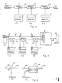
- Fig. 4 is a block diagram indicating the principle structure of the present invention.
- the light emitting source laser diode or LED(Light Emitting Diode)
- the light emitting source is provided to the one end of an optical fiber 20 which forms the optical bus and the DC light of a constant level is always input to the optical fiber from such light source 10.
- Each terminal sends data through modulation of DC light on the optical bus by turning ON and OFF the optical switch corresponding to the sending data on the occasion of sending data to the optical bus.
- an optical level at the optical receiver provided at the other end of optical bus is constant and it is no longer necessary to adjust optical level, at the optical receiver, of sending optical signal from each terminal.
- the optical receiver is not required to have wide dynamic range and high speed response of automatic gain control function can be realized.
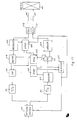
- Fig. 5 is an embodiment where the principle structure of Fig. 4 is adopted to the ISDN user network.
- the light souce 10 (laser diode or LED) is provided at the one end of sending bus 20 of each terminal interfaces 1 ⁇ n and optical switches 11 ⁇ 1n are provided to the sending bus 20 in place of optical couplers 31 ⁇ 3n.
- Each terminal interfaces 1 ⁇ n controls for ON and OFF the optical switches 11 ⁇ 1n corresponding to the sending data on the occasion of sending data to the user network interface 41.
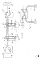
- Fig. 6(a) is an optical coupler consisting of a half-mirror 151, which reflects a part of incident light to send to the side of terminal and allows the other part of incident light to transmit for reinput to the optical bus 40.
- Fig. 6(b) is a waveguide type optical coupler wherein an optical waveguide 153 consisting of SiO2 is formed on a Si substrate 152.
- Figs. 7(a),(b) is diagrams for explaining structure and operation of optical switches 11 ⁇ 1n.
- the optical switches 11 ⁇ 1n can be changed to the condition, as indicated in Fig. 7(a), where optical signal is output to the output terminal d from the input terminal a and to the output terminal c from the input terminal b and to the condition, as indicated in Fig. 7(b), where optical signal is output to the output terminal c from the input terminal a and to the output terminal d from the input terminal b.
- optical switches 11 ⁇ 1n can be realized by the switching structure where optical fiber and prism are mechanically moved or electrical/optical effect is used.
- the optical switch utilizing electrical/optical effect has the structure indicated in Fig. 7(c), wherein the optical waveguide paths 211 are crossed by diffusing Ti, etc. on a substrate 10 of electrical/optical effect material such as LiNbO3, etc., the electrodes 212, 213 are formed so that the electrical field is applied to such crossing area and the terminals 214, 215 are connected to these electrodes 212, 213.
- the DC light on the sending optical bus 20 is digitally modulated by, as indicated in Fig. 7(c), connecting an optical fiber which forms sending optical bus 20 to the input and output terminals b and c, also connecting the anti-reflection termination 121 to the output terminal d and changing voltages V1, V2 applied to the optical switches in accordance with digital signals "0" and "1".
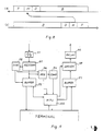
- Fig. 8(a) is a frame format on the receiving bus 40, while (b) is a frame format on the sending bus 20.
- the frame is formed by the D channel for calling and controlling send destination party and the B channel for loading data. These channels are led by the frame synchronous signal F and the monitor bit M with which each terminal can obtain the D channel.
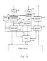
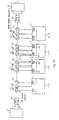
- Fig. 9 is a block diagram of the terminal interface and Fig. 10 is a block diagram of the user network interface 41.
- the data on the sending bus is partly input to the optical/electrical converting circuit 91 provided in the terminal interface through optical couplers 21 ⁇ 2n, it is then converted to electrical signal and the waveform of this signal is then shaped by the receiver 93.
- the frame synchronous circuit 92 receives an output of the receiver 93 and outputs various timing signals through frame synchronization with the frame synchronous signal.
- the monitor bit M ⁇ and the D channel information are set to the register 94 by the timing signal from the frame synchronous circuit 92.
- the microprocessor 100 checks the monitor bit M ⁇ and content of D channel set to the register 94. If vacant condition of D channel is detected by the check of monitor bit M ⁇ , the D channel can be obtained.
- the microprocessor 100 controls ON and OFF the optical switches 11 ⁇ 1n in order to set own discrimination signal to the monitor bit M on the sending bus.
- This control is carried out as explained hereunder. Namely, the leading address of buffer 97 stores the monitor bit M and frame synchronous signal pattern F. Therefore, these are read and an optical switch driver 98 is also driven.
- the optical switch driver 98 outputs voltages V1, V2 in accordance with content of monitor bit M and frame synchronous signal F read from the buffer 97.
- An output voltage of optical switch driver 98 is applied to the optical switch through a delay circuit 99, controlling ON and OFF the optical switch (correspond ing to Figs. 7(a),(b)). Thereby, the DC light on the sending bus 20 becomes the optical signal containing the frame synchronous signal F and monitor bit M.
- the monitor bit M is extracted and this monitor bit M is directly returned to the receiving bus. Namely, the returned monitor bit M is loaded on the monitor bit M ⁇ .
- the monitor bit M ⁇ is set to the register 94 and is moreover input to a comparator 96.
- the comparator 96 always holds content of monitor bit M transmitted and it is then compared with the monitor bit M ⁇ input from the register 94. A result of such comparison is then sent to the microprocessor 100.
- the microprocessor 100 detects that it has loaded the signal for access to the D channel and knows it has the right of making access to the D channel.
- the frame synchronous pattern F, monitor bit M and signal for D channel being stored in the buffer 97 are read therefrom, and is then input to the optical switch driver 98 for the control of optical switch to ON and OFF states.
- the signal for D channel means the control information (digital signal) which indicates dial pulse or termi nation, etc. to be used by switching equipment 46 for line connection, and this D channel signal and B channel signal are sent to the switching equipment 46 through the subscriber network interface 41 and the subscriber line 45.
- the data is also loaded to the monitor bit M for the D channel access simultaneously from the other terminal interface suggesting generation of data collision.
- the MPU 100 loads the data to the monitor bit M for repeated access to the D channel after the specified period (the time detemrined in accordance with some random numbers).
- the MPU 100 In case the MPU 100 known that it is called by checking the D channel on the receiving bus, it stores the signal of B channel on the receiving bus and transfers it to the terminal.
- a delay circuit 99 is provided in each terminal interface because of the reason explained hereunder.
- the transmission time from subscriber network interface 41 to respective terminal interfaces l ⁇ n is t1, t2,....., t n
- an internal delay time from reception of data on the receiving bus to start of modulation of DC light on the sending bus at the respective terminal interfaces 1 ⁇ n is T o
- delay time from optical switches 11 ⁇ 1n of respective terminal interfaces 1 ⁇ n to subscriber network interface 41 is T1, T2, Vietnamese, T n , following relation can be obtained.
- t n + T n + T o + ⁇ n in order to correctly receive (the signals transmitted from respective terminal interfaces 1 ⁇ n are not overlapped) the frame format indicated in Fig. 8(b) on the sending bus at the optical/electrical converting circuit in the user network interface 41.
- the delay circuit 99 conceives intrinsic delay time ⁇ 1, ⁇ 2,...., ⁇ n for respective terminal interfaces 1 ⁇ n.
- the ISDN user network is connected with the digital switching equipment 46 from the interface 41 (not illustrated), through the optical fiber 45, 45 ⁇ , consisting the subscriber line.
- the frame from switching equipment 46 are transmitted by optical fibert 45 ⁇ , converted into electrical signal by O/E converter 109, and input to receiver 103.
- the frame from user network interface 41 is converted into optical signal by E/O converter 110, and transmitted to the switching equipment 46 via optical fiber 45.
- the received data is input to the frame synchronous circuit 104 for frame synchronization.
- the frame synchronous circuit 104 generates various timing signals on the basis of synchronoized clock.
- the data received by the receiver 103 is stored in the buffer 114, read by the timing signal sent from the frame synchronous circuit 104, input to the electrical/optical converting circuit 43 through the OR circuit 113, converted to optical signal therein and is then transmitted to the receiving bus 40.
- the optical signal on the sending bus 20 is converted to the electrical signal by the photoelectric converting circuit 42 and is then input to the receiver 107.
- the receiver 107 shapes the waveform of received signal.
- the frame synchronization is established by the frame synchronous circuit 106.
- the frame synchronous circuit 106 switches the selector 111 to the register side in order to set the monitor bit M indicated in Fig. 8(b) to the register 105. Since the information other than the monitor bit M is transmitted to the switching equipment 46 by the driver 48, the selector 111 is switched to the driver side at the positions other than the monitor bit M.
- the driver 108 amplifies the signal sent from the receiver 107. This signal is transmitted to the optical fiber 45 by the E/O 110 and is then sent to the switching equipment 46.
- the frame synchronous circuit 104 outputs the timing signal which indicates the end timing of the frame synchronous pattern to the register 105 in order to send the monitor bit M set to the register 105 to the receiving bus 40 following the frame synchronous pattern of data received by the receiver 103 and then inputs the monitor bit M to the electrical/optical converting circuit 43 through the OR circuit 113.
- the D channel and B channel data following the frame synchronous pattern stored in the buffer 114 are read and are input to the electrical/optical converting circuit 43 through the OR circuit 113. Operations of Fig. 5 are explained above.
- the ISDN subscriber network indicated in Fig. 11 has solved such problem. Namely, the other end of receiving bus 40 receives the optical signal of the frame format indicated in Fig. 8(a) transmitted on the receiving bus 40 from the subscriber network interface 41 by the optical/electrical signal converter 50.
- the frame synchronous signal generator 51 the same frame synchronous pattern synchronized with the received frame synchronous pattern is output to the electrical/optical converting circuit 52 and the frame synchronous pattern is transmitted to the sending bus 20.
- the respective terminal interface monitors the frame synchronous pattern on the sending bus 20 through the optical couplers 31 ⁇ 3n provided to the sending bus 20 for establishing frame synchronization and sends only the monitor bit M, D channel and B channel signals indicated in Fig. 8(b).
- the frame synchronous pattern on the receiving bus 40 is transmitted to the sending bus 20 in such a form as returning in order to eliminate variation due to difference of accommodating positions of respective terminals by making equal the sum of times T + T ⁇ + T ⁇ , wherein T is the period from the timing of sending the frame synchronous pattern to the receiving bus 40 from the subscriber network interface 41 to the timing of detecting this frame synchronous pattern by respective terminal interfaces, T ⁇ is the period from the timing of sending the frame synchronous pattern to the sending bus 20 from the frame synchronous signal generating circuit 51 to detecting such frame synchronous pattern by respective terminal interface and starting transmission of data by optical switches 11 ⁇ 1n and T ⁇ is the propagation time of optical signal from the optical switches 11 ⁇ 1n to subscriber network interface 41.
- frame synchronous signal generating circuit 51 in Fig. 11 is explained with reference to Fig. 12 and the structure of terminal interface to Fig. 13.
- the data on the receiving bus 40 converted to electrical signal by the photoelectric converting circuit 50 is shaped in the waveform by the receiving circuit 511 and frame synchronization is established by the frame synchronous circuit 512.
- the frame synchronous circuit 512 outputs the timing signal to the frame synchronous pattern generating circuit 513 at the frame synchronous pattern detecting position, causing it to output the frame synchronous pattern.
- this frame synchronous pattern is output in synchronization with the clock signal output from the frame synchronous circuit 513.
- the frame synchronous pattern output from the frame synchronous pattern generating circuit 513 is converted to optical signal by the electrical/optical signal converting circuit 52 through the gate circuit 514 and is then transmitted to the sending bus 20.
- the frame synchronous pattern generating circuit 513 continuously outputs a high level or low level signal in order to cause the electrical/optical signal converting circuit 52 to output the DC light.
- Fig. 13 is almost same as the structure of Fig. 9 and provides the optical/electrical converting circuit 101, receiver 102 and frame synchronous circuit 92 in order to establish frame synchronization by detecting frame synchronous pattern on the sending bus 20.
- the frame synchronous circuit 92 outputs the timing signal which indicates the frame synchronous pattern end position on the sending bus 20 to the buffer 97 and optical switch driver 98. Thereby, it becomes possible to send the data by controlling the optical switches 11 1n, following the frame synchronous pattern on the sending bus 20.
- the sending bus and receiving bus are respectively necessary.
- the sending bus and receiving bus can be used in common to each other by employing so-called ping-pong transmission system and the scale of hardware can be reduced.
- Fig. 14 is an example of system structure in case the sending bus and receiving bus are used in common in order to make small and scale of hardware.
- Fig. 15 is a time chart of signals on the bus.
- the frame is allowed by the end flag E for correspondence to variable length frame.
- Fig. 14 is an embodiment where the up-frame is synchronized with the down-frame.
- the frame synchronous signal generating circuit 51 having the function to return the frame is provided at the other end of bus and moreover second optical couplers 31 3n are also provided as the means for receiving and detecting the up-frame signal with respective terminal interfaces.
- the frame synchronous signal generating circuit 51 establishes frame synchronization using the frame signal of the down-signal obtained through the optical/electrical convertion (O/E) element. After detection of end flag E, the frame synchronous signal of up-frame indicated in Fig. 15 is transmitted and the DC light is transmitted after the monitor bit M.
- the second optical couplers 31 ⁇ 3n fetch such up-frame signal and the optical communication information is obtained by causing the relevant optical switches 11 - 1n to make switching operation by the communication information to be sent to the subscriber network interface 41 from respective terminals during establishment of frame synchronization. Reception of down-channel information is carried out in the same way as Fig. 5 and Fig. 11. This embodiment can also be used for maintenance because the second optical couplers 31 ⁇ 3n can also be used as the monitoring means for the sending optical communication information (signals modulated by the optical switches 11 ⁇ 1n) of own station.
- Fig. 16 is a block diagram of the frame synchro obviously signal generating circuit 51 in Fig. 14.
- the detecting circuit 515 switches the optical switch 53 to the side of electrical/optical converting circuit 52, opens the gate circuit 514 and informs the frame synchronous circuit 512 of start of up-frame period.
- the successive operations are same as that in Fig. 12.
- the end flag E in the up-frame is added to the end of frame of sending data by the respective terminal interfaces which send data suing the D channel and B channel.
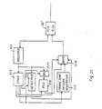
- Fig. 17 is a block diagram of the subscriber network interface 41 of Fig. 14.
- the structure of Fig. 17 is almost the same as that of Fig. 10 but the structure for ping-pong transmission control is added. This structure is explained hereunder.
- an output of optical switch 47 is connected with the optical/electrical converting circuit 42.
- the end flag E of up-frame is detected by the detecting circuit 112 which operates in synchronization with the clock signal of frame synchronous circuit 106.
- the detecting circuit 112 switches the optical switch 47 to the side of electric/optical converting circuit 43 and informs the frame synchronous circuit 104 of start of sending the down-frame.
- the frame synchronous circuit 104 reads the data stored in the buffer 114, detects the end position of frame synchronous pattern and adds the monitor bit M ⁇ to the trailing part of frame synchronous pattern, thus reading the monitor bit M from the register 105 and outputting it to the electrical/optical converting circuit 43.
- the successive operations are the same as those of Fig. 10.
- the detecting circuit 112 has the function to count up the clock signal sent from the frame synchronous circuit 106 and monitors the detecting time from detection of frame synchronous pattern F to the end flag E. If the end flag E is not detected within the maximum allowable period, it is judged as that no data has been transmitted from respective terminal interfaces and the signal for sending the data stored in the buffer 114 is output to the frame synchronous circuit 104 for switching the transmission of the down-frame.
- optical bus type communication system indicated in Fig. 14 used only a single line of optical fiber, it has eliminated one of said problems but since one optical switch and two optical couplers are used, further simplication of facilities and reduction in cost are necessary.
- Fig. 18 is a system structure for eliminating said problem.
- the user network interface 41 and a plurality of temrinals 1-1, 1-n are bus-connected through a single line of optical fiber cable and the furthest end is provided with the frame synchronous signal generating circuit 51.
- the optical fiber cable is provided with one optical switch 1n (11) and one optical coupler 2n ⁇ (21) for each terminal.
- the optical coupler 2n ⁇ has the quadruple directivity and functions as the optical coupler for data reception which allows transmission of up-signal and down-signal of the user network interface 41 and each terminal and also functions as the optical coupler for receiving sending frame. Namely, two optical couplers 31, 21, ...., 3n, 2n of Fig. 14 are reduced to only one optical coupler 2n ⁇ , 21.
- the optical switch 1n is connected with terminal through a conductive line 71c.
- Other terminals are also connected with the optical coupler and optical switch in the same way.
- the optical switch 1n may be provided in any side of the user network interface 41 or frame synchronous signal generating circuit 51 for the optical coupler 2n ⁇ . In case it is provided to the side of frame synchronous signal generating circuit 51, the switching control of optical switch 1n can be realized while setting frame synchronization with the receiving data in the up-frame and thereby timing control can be realized easily. In case the optical switch 1n is provided in the side of user network interface, an output of optical switch 1n can be monitored by the optical coupler 2n ⁇ for maintenance and self-diagnosis. In above explanation of operations, the temrinal 1-n is considered as an example but this explanation can also be adopted to the other terminals.
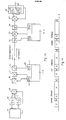
- LED is used as the transmitter and receiver of optical signal.
- LED gene rally has the functions as the light emitting element and light sensitive element.
- the O/E converting circuit and E/O converting circuit can be integrated. Namely, the O/E.E/O converting circuit can be realized with only one LED and thereby further cost reduction can be attained.
- the light sending and receiving circuit of Fig. 19 can be adapted to Fig. 16 by connecting an output of the gate circuit 514 to the IN terminal, OUT terminal to the receiver 511 and then optically coupling the sending/receiving bus with the LED.
- the gate circuit 514 since the gate circuit 514 is always closed during reception of the down-frame, no data is input to the IN terminal of Fig. 19 and therefore the LED does not emit the light during reception of light.
- the sending and receiving bus may directly be coupled with the LED and optical switch 53 may be eliminated because sending and receiving of light are not conducted simultaneously.
- Fig. 18(b) is a diagram for explaining the connecting mode of optical coupler of Fig. 18(a).
- the optical signal (indicated by arrow mark of solid line) input from the terminal a is output to the terminal C and it is partly branched and is output to the D terminal. Therefore, the down-frame sent from the subscriber network interface can be monitored by connecting the sending/receiving bus to the terminals a, C and optical/electrical converting circuit 91 for monitoring receiving bus (down-frame) to the terminal D.
- the optical signal (indicated by arrow mark of dotted line) input from the terminal C is output to the terminal a and it is partly branched and is then output to the terminal b. Accordingly, the frame synchronous pattern of up-frame returned from the frame synchronous signal generating circuit 51 can be monitored by connecting the optical/electric converting circuit 101 for monitoring sending bus (up-frame) to the terminal b. Thus, both up-frame and down-frame can be monitored only with one optical coupler.
- the sub scriber network interface 41 and frame synchronous signal generating circuit 51 respectively require the optical/electrical covnerting circuits 42, 50, electrical/optical converting circuits 43, 52 and optical switches 47, 53 which executes switching of optical paths for the ping-pong transmission.
- the light sending and sensitive circuit of Fig. 19 can also be adopted to the user network interface circuit 41 of Fig. 17.
- the end of optical fiber 40 is returned and is connected to the optical fiber 20, thereby forming a loop network around the subscriber network interface 41.
- the structure of user network interface 41 in Fig. 20 is almost the same as Fig. 17, but the frame synchronous pattern generating circuit 114 and DC light sending function are added. These components are explained hereunder.
- the detecting circuit 112 detects the end flag of the down-frame (receiving frame), the time for sending the up-frame starts, sending the frame synchronous pattern and following DC light. Therefore, the detecting circuit 112 controls the gate circuit 113, connecting an output of frame synchronous pattern generating circuit 114 to the electrical/optical converting circuit 43. In this case, the detecting circuit 112 outputs the signal for detecting the end flag E to the frame synchronous circuit 104.
- the frame synchronous circuit 104 sends the clock signal to the frame synchronous patern generating circuit 114, also outputs the frame synchronous pattern to the electric/optical converting circuit 43 and continuously outputs the high level or low level signal to cause the electric/optical converting circuit 43 to output DC light, after sending the frame synchronous pattern.
- Other operations are carried out in the same way as Fig. 17.
- the frame format of receiving bus 40 is employed and the frame format of sending bus 20 is employed as indicated in Fig. 22(b).
- the I, I ⁇ channels for extension line communication are provided at the trailing part of B channel.
- the I, I ⁇ channels is composed of the CONT area which indicates address information including the sending and receiving terminals and the DATA area loading sending information.
- the special pattern for discriminating I, I ⁇ channels is added and thereby respective terminal interface and user network interface 41 are capable of discriminating reception of the I, I ⁇ channels through detection of such special pattern.
- the procedures for accessing I, I ⁇ channels the well known CSMA/CD system can be employed.
- the extension line communication by the CSMA/CD system can be realized by loading the I channel information set on the sending bus 20 to the I ⁇ channel and returning it to the receiving bus 40 for reception by respective terminal interfaces. Therefore, the user network interface 41 is required to have the I channel returning function. This function can be realized with the structure similar to the monitor bit M returning part.
- the data transmitted to the sending bus is received by the receiving bus, the sending data is compared with the receiving data. When these are matched, it is discriminated that the da has been transmitted normally. If these are not matched, it is judged that the sending data has collided with the sending data from the other terminal interface and the same data is transmitted again. Therefore, each terminal interface is required to provide the function to detect the special pattern added to the leading region of the CONT area of I channel and the function to compare content of I channel with that of I ⁇ channel.
- the special pattern detecting function can be realized with the structure similar to the end flag explained with reference to Fig. 16, Fig. 17 and Fig. 21.
- Fig. 23 is the frame format.
- Fig. 23(a) indicates the down-frame while (b) the up-frame.
- Fig. 24 indicates an example of system structure.
- the second monitor bits M o , M o ⁇ for making access to the I channel are provided.
- the user network interface 41 extracts the special patternin the CONT area of up-frame and loads it to the monitor bit M o ⁇ and returns it as in the case of the monitor bit M described previously, thereby obtaining the right for access to I channel.
- the frame synchronous signal generating circuit 51 also extracts the special pattern of CONT area of the down-frame and then returns it by loading it to the monitor bit M o .
- the structure of user network surface circuit 41 can be realized with the same structure of Fig. 21. In this case, however, the function to send the DC light at the position of I ⁇ channel is necessaryy. Structure of the frame synchronous signal generating circuit 51 and structure of terminal interface are indicated in Fig. 25 and Fig. 26.
- the terminal interface 3 receives the down-frame with the receiver 81 through the optical/electric converting circuit 101 during the period for sending the down-frame from the user network interface 41.
- the frame synchronous circuit 92 establishes the frame synchronization by the frame synchronous pattern of the received down-frame and outputs various timing signals for discriminating bit positions of down-frame.
- the frame synchronous circuit 92 opens the gate 84 at the position of monitor bit M ⁇ and sets the monitor bit M ⁇ to the register 96.
- the comparator 94 holds the monitor bit M transmitted during access to the D channel and compares such monitor bit M with the monitor bit M ⁇ set to the register 96.
- the successive operations are same as that of Fig. 9.
- Fig. 26 during use of the D channel, it is stored in the buffer 95 and is then transferred to the terminal because the gate opens at the position of D channel and B channel through the timing control of the microprocessor 100 and frame synchronous circuit 92.
- the frame synchronous circuit 92 sends the timing signal to the gate 85 at the position of the monitor bit M o ⁇ and sets the monitor bit M o ⁇ to the register 88. Thereafter, the frame synchronous circuit 92 sets the next CONT area to the register 87 through the gate 86. Moreover, the circuit 92 stores the DATA ara of I channel to the buffer 95 through the gate 92.
- the microprocessor 100 reads the content (CONT) of register 87 and detects that the data has been sent to the terminal accommodated in the terminal interface 3 and then sends the DATA area of I channel stored in the buffer 95 to the temrinal.
- CONT content
- the terminal interface 3 receives the data to own terminal in the I channel within the period of down-frame.
- the microprocessor 100 detects vacant condition of I channel by checking CONT area. If the data for extension line communication is stored in the buffer 97, the microprocessor 100 reads the content (CONT + DATA + E) of I ⁇ channel to be transmitted from the buffer 97 and sends it to the driver 98, loading the data to the I ⁇ channel by controlling the optical switch 33 to the ON and OFF state.
- the terminal interface 2 also receives the down-frame, in the same way, from the optical coupler 22 through the optical/electric converting circuit 101.
- the data of I ⁇ channel transmitted from the terminal interface 3 is destinated to the terminal accommodated in said terminal interface 2.
- the microprocessor 100 detects it from the content of CONT area being set to the register 87 and transfers data of DATA area stored in the buffer 95.
- the response data to the received data of I ⁇ channel is transmitted to the terminal interface 3 within the period of the next up-frame.
- the frame synchronous circuit 512 sends the timing signal to the selector 517 at the position of special pattern of CONT area and sets such special pattern to the register 516.
- the detecting circuit 515 detects the end flag E of down-frame, the time of up-frame starts.
- the frame synchronous circuit 512 sends the timing signal to the frame synchronous pattern generating circuit 513 through the gate circuit 514 so that the electric/optical converting circuit 50 continuously sends the high level or low level signal required for outputting the DC light during the periodf rom the end of frame synchronous pattern F to the end of up-frame.
- the frame synchronous circuit 512 sends the timing signal for outputting content of special pattern being set to the register 516 and controls the gate circuit 514 to select the output of register 516 only during the period of monitor bit M o . Therefore, the up-frame is sent to the sending/receiving bus under the condition that the special pattern is loaded on the monitor bit M o and the DC light is loaded on the I channel.
- the terminal interface 2 receives the up-frame at the optical/electric converting circuit 91 through the optical coupler 32 ⁇ .
- the receiver 93 shapes waveform of the received up-frame signal. In case the vacant condition of I channel is detected from the content of CONT area being set to the register 111, the receiver 93 controls the optical switch 12 for ON and OFF state and loads the send data to the I channel.
- the terminal interface 3 receives the up-frame at the optical/electric covnerting circuit 91 through the optical coupler 33 ⁇ .
- the monitor bit M o returned by the frame synchronous signal generating circuit 51 under the control of frame synchronous circuit 92 is set to the register 106.
- the comparator 109 holds the special pattern returned by said down-frame and compares such special pattern with the content of register 106.
- the microprocessor 100 judges that preceding data transmission has completed normally in case the comparison result matches. If it does not match, it means that some trouble has occurred. In this case, the data is transmitted again or fault analysis is carried out.
- extension line communication can be realized only with simple hardware structure and moreover the down-frame and up-frame channels can be used by two terminal interfaces.
- Fig. 27 is a system structure in case the extension line communication between terminals is carried out with the system structure of Fig. 11. In this case, the extension line communication is carried out using the frame format of Fig. 23.
- the structure of subscriber network interface 41 is the same as that of frame synchronous signal generating circuit 51.
- the down-frame on the receiving bus 40 is branched to the terminal interfaces 1, 2, 3, Vietnamese, n by the optical couplers 21, 22, Vietnamese, 2n.
- data is loaded to the I ⁇ channel by controlling the optical switches 12 ⁇ , 13 ⁇ , whil, 1n ⁇ for ON and OFF state.
- the up-frame on the sending bus 20 is branched to the terminal interfaces 1, 2, 3, ...., n by the optical couplers 31, 32,...., 3n.
- data is loaded to the I channel by controlling the optical switches 11, 12, 1n-1 for ON and OFF state.
- the terminal interface 1 is not provided with the optical switch on the receiving bus 40 and the terminal interface n is not provided with the optical switch on the sending bus 20 because the terminal interfaces 1 ⁇ n cannot realize extension line communication using the receiving and sending bus as is obvious from Fig. 27.
Landscapes
- Engineering & Computer Science (AREA)
- Computer Networks & Wireless Communication (AREA)
- Signal Processing (AREA)
- Small-Scale Networks (AREA)
- Optical Communication System (AREA)
Applications Claiming Priority (8)
| Application Number | Priority Date | Filing Date | Title |
|---|---|---|---|
| JP203430/86 | 1986-08-29 | ||
| JP20343086 | 1986-08-29 | ||
| JP27570786 | 1986-11-19 | ||
| JP275707/86 | 1986-11-19 | ||
| JP6460/87 | 1987-01-14 | ||
| JP646087 | 1987-01-14 | ||
| JP8901087 | 1987-06-11 | ||
| JP89010/87 | 1987-06-11 |
Publications (3)
| Publication Number | Publication Date |
|---|---|
| EP0262409A2 true EP0262409A2 (de) | 1988-04-06 |
| EP0262409A3 EP0262409A3 (en) | 1989-07-26 |
| EP0262409B1 EP0262409B1 (de) | 1993-12-08 |
Family
ID=27454493
Family Applications (1)
| Application Number | Title | Priority Date | Filing Date |
|---|---|---|---|
| EP87112547A Expired - Lifetime EP0262409B1 (de) | 1986-08-29 | 1987-08-28 | Optisches Busübertragungssystem |
Country Status (4)
| Country | Link |
|---|---|
| US (1) | US4850047A (de) |
| EP (1) | EP0262409B1 (de) |
| CA (1) | CA1278042C (de) |
| DE (1) | DE3788403T2 (de) |
Cited By (3)
| Publication number | Priority date | Publication date | Assignee | Title |
|---|---|---|---|---|
| EP0545401A3 (en) * | 1991-12-05 | 1993-09-29 | Canon Kabushiki Kaisha | Optical integrated nodes, and optical communication systems and networks using the optical integrated nodes |
| EP0689067A3 (de) * | 1994-06-22 | 1997-04-09 | Fujitsu Ltd | Herstellungsverfahren für ein optisches Wellenleitersystem, optisches Bauelement und optischer Koppler mit dessen Verwendung, optisches Netzwerk und optische Leiterplatte |
| US5854868A (en) * | 1994-06-22 | 1998-12-29 | Fujitsu Limited | Optical device and light waveguide integrated circuit |
Families Citing this family (28)
| Publication number | Priority date | Publication date | Assignee | Title |
|---|---|---|---|---|
| US5247380A (en) * | 1988-01-27 | 1993-09-21 | Spectrix Corp | Infrared communications network |
| US5099346A (en) * | 1988-01-27 | 1992-03-24 | Spectrix Corporation | Infrared communications network |
| US5165077A (en) * | 1989-02-28 | 1992-11-17 | Fujitsu Limited | Optical drop-and-insert apparatus |
| US5050164A (en) * | 1989-10-31 | 1991-09-17 | Bell Communications Research, Inc. | Optical customer premises network |
| US5325376A (en) * | 1990-02-23 | 1994-06-28 | Canon Kabushiki Kaisha | Communication system for detecting a communication error in information transmitted between a plurality of units and a main control unit |
| EP0452895B1 (de) * | 1990-04-18 | 1996-07-03 | Canon Kabushiki Kaisha | Optisches Übertragungsnetzwerk und Übertragungsverfahren für dasselbe |
| JPH0671266B2 (ja) * | 1990-06-01 | 1994-09-07 | 日本航空電子工業株式会社 | 光トランシーバ |
| WO1991020138A1 (en) * | 1990-06-14 | 1991-12-26 | Light Wave Communications, Inc. | Fiber optic communication of three-level electronic signals |
| US5287353A (en) * | 1991-12-23 | 1994-02-15 | Square D Company | Apparatus for generating and sending a serial data packet for controlling a network of single point I/O devices |
| US5267240A (en) * | 1992-02-20 | 1993-11-30 | International Business Machines Corporation | Frame-group transmission and reception for parallel/serial buses |
| US5455831A (en) * | 1992-02-20 | 1995-10-03 | International Business Machines Corporation | Frame group transmission and reception for parallel/serial buses |
| DE19620723A1 (de) * | 1996-05-23 | 1997-11-27 | Sel Alcatel Ag | Optische Netzwerkeinheit und Zentrale eines optischen Kommunikationsnetzes |
| US5719975A (en) * | 1996-09-03 | 1998-02-17 | Hughes Electronics | Optically reconfigurable conductive line element |
| US5898801A (en) | 1998-01-29 | 1999-04-27 | Lockheed Martin Corporation | Optical transport system |
| DE19810290A1 (de) * | 1998-03-10 | 1999-09-16 | Bayerische Motoren Werke Ag | Datenbus für mehrere Teilnehmer |
| JP2000147306A (ja) * | 1998-08-31 | 2000-05-26 | Kokusai Electric Co Ltd | 波長領域多重光スタ―カプラ、通信局、及び光伝送システム |
| US20020101874A1 (en) * | 2000-11-21 | 2002-08-01 | Whittaker G. Allan | Physical layer transparent transport information encapsulation methods and systems |
| FR2837296B1 (fr) * | 2002-03-15 | 2004-06-25 | Airbus France | Dispositif et procede d'acquisition de mesures a l'aide d'un bus de communication numerique, utilises notamment lors des essais d'un aeronef |
| US7085497B2 (en) | 2002-04-03 | 2006-08-01 | Lockheed Martin Corporation | Vehicular communication system |
| US20040076434A1 (en) * | 2002-09-27 | 2004-04-22 | Whittaker G. Allan | Optical distribution network for RF and other analog signals |
| US6912339B2 (en) * | 2002-09-27 | 2005-06-28 | Lockheed Martin Corporation | Optical interface devices having balanced amplification |
| US7283480B1 (en) | 2002-11-12 | 2007-10-16 | Lockheed Martin Corporation | Network system health monitoring using cantor set signals |
| US7349629B1 (en) | 2002-11-26 | 2008-03-25 | Lockheed Martin Corporation | Methods and systems for creating a digital interconnect fabric |
| US7424228B1 (en) | 2003-03-31 | 2008-09-09 | Lockheed Martin Corporation | High dynamic range radio frequency to optical link |
| WO2004093351A2 (en) * | 2003-03-31 | 2004-10-28 | Lockheed Martin Corporation | Optical network interface systems and devices |
| US7440699B1 (en) | 2004-06-28 | 2008-10-21 | Lockheed Martin Corporation | Systems, devices and methods for transmitting and receiving signals on an optical network |
| EP2494713B1 (de) * | 2009-10-29 | 2016-05-18 | Hewlett-Packard Development Company, L. P. | Optischer datenbus und verfahren |
| IN2013MU01980A (de) * | 2013-06-10 | 2015-05-29 | Indian Inst Technology Bombay |
Family Cites Families (6)
| Publication number | Priority date | Publication date | Assignee | Title |
|---|---|---|---|---|
| US4002898A (en) * | 1976-01-26 | 1977-01-11 | The United States Of America As Represented By The Secretary Of The Navy | Single mode laser multiterminal optical data communication system |
| ATE13788T1 (de) * | 1980-12-17 | 1985-06-15 | Ici Plc | Vorrichtung zum zusammenfassen von daten aus mehreren zustandsabhaengigen optischen sensoren. |
| GB8503881D0 (en) * | 1984-03-29 | 1985-03-20 | Singer Co | Optical switching arrangement |
| JPS62749A (ja) * | 1985-06-27 | 1987-01-06 | Mitsubishi Electric Corp | 換気扇装置 |
| ID20397A (id) * | 1997-05-26 | 1998-12-03 | Hoechst Ag | Pemurnian kompleks transkripsi tingkat lebih tinggi dari hewan bukan manusia transgenik |
| JPH113401A (ja) * | 1997-06-12 | 1999-01-06 | Canon Inc | 情報処理装置及びその方法 |
-
1987
- 1987-08-19 US US07/086,807 patent/US4850047A/en not_active Expired - Fee Related
- 1987-08-28 DE DE3788403T patent/DE3788403T2/de not_active Expired - Fee Related
- 1987-08-28 CA CA000545592A patent/CA1278042C/en not_active Expired - Lifetime
- 1987-08-28 EP EP87112547A patent/EP0262409B1/de not_active Expired - Lifetime
Cited By (6)
| Publication number | Priority date | Publication date | Assignee | Title |
|---|---|---|---|---|
| EP0545401A3 (en) * | 1991-12-05 | 1993-09-29 | Canon Kabushiki Kaisha | Optical integrated nodes, and optical communication systems and networks using the optical integrated nodes |
| US6072925A (en) * | 1991-12-05 | 2000-06-06 | Canon Kabushiki Kaisha | Optical integrated nodes, and optical communication systems and networks using the optical integrated nodes |
| EP0689067A3 (de) * | 1994-06-22 | 1997-04-09 | Fujitsu Ltd | Herstellungsverfahren für ein optisches Wellenleitersystem, optisches Bauelement und optischer Koppler mit dessen Verwendung, optisches Netzwerk und optische Leiterplatte |
| US5854868A (en) * | 1994-06-22 | 1998-12-29 | Fujitsu Limited | Optical device and light waveguide integrated circuit |
| US6081632A (en) * | 1994-06-22 | 2000-06-27 | Fujitsu Limited | Method of producing optical waveguide system, optical device and optical coupler employing the same, optical network and optical circuit board |
| EP1315006A1 (de) * | 1994-06-22 | 2003-05-28 | Fujitsu Limited | Verfahren zur Herstellung von Wellenleitersystemen, dessen Verwendung in optischem Bauelement und Koppler sowie optisches Netzwerk und optische Leiterplatte |
Also Published As
| Publication number | Publication date |
|---|---|
| DE3788403D1 (de) | 1994-01-20 |
| DE3788403T2 (de) | 1994-05-11 |
| US4850047A (en) | 1989-07-18 |
| EP0262409B1 (de) | 1993-12-08 |
| CA1278042C (en) | 1990-12-18 |
| EP0262409A3 (en) | 1989-07-26 |
Similar Documents
| Publication | Publication Date | Title |
|---|---|---|
| EP0262409B1 (de) | Optisches Busübertragungssystem | |
| CA1193691A (en) | Multiple access data communication system control | |
| GB2131252A (en) | System and method for controlling a multiple access data communications system | |
| GB2166328A (en) | In-house distribution facility for a broadband communication system | |
| CA2023446C (en) | Packet communication method, packet communication device and packet switcher | |
| KR900006322B1 (ko) | 디지탈 가입자 라인 시험장치를 갖는 디지탈 회로망 시스템 | |
| EP0981261A3 (de) | Belastungsbalancierte UBR Leitweglenkung in ATM Netzen | |
| EP0380341B1 (de) | Optisches Übertragungssystem | |
| US6944132B1 (en) | Transmission apparatus, order wire transmission system and order wire monitoring method | |
| CA2063536C (en) | Terminal equipment and optical communication system using the same | |
| US5309440A (en) | ISDN user-network interface system | |
| CA2051146C (en) | Integrated services digital network (isdn) terminal having diagnostic function | |
| US6014369A (en) | Method and apparatus for testing subscribers accommodated to service node in loop system | |
| JPH03503350A (ja) | 情報を1つの伝送区間に分散的に送出するための方法および装置 | |
| Gerla et al. | Token-based protocols for high-speed optical-fiber networks | |
| RU2115245C1 (ru) | Способ контроля оптических широкополосных соединительных линий вплоть до пассивного стыка | |
| US20020091864A1 (en) | Ring network being installed as bus network | |
| RU2116007C1 (ru) | Устройство приема тактовых сигналов для управления сетевой синхронизацией атс | |
| EP0403455A2 (de) | Vorrichtung zur Steuerung der Bandbreite in einer Übertragungseinrichtung mittels Monomodenfaser, unabhängig vom Signalformat | |
| JP3435560B2 (ja) | 終端装置 | |
| EP0898832B1 (de) | Verfahren und detektoreinheit zum verbindungsaufbau in einem fernübertragungsnetz | |
| Kohashi et al. | Integrated-circuit and packet-switching applications to a loop system for local area networks | |
| JP2906823B2 (ja) | 光加入者伝送システム及び加入者時分割双方向通信システム | |
| JPH0527318B2 (de) | ||
| Inbar | Optical channels in distributed processing |
Legal Events
| Date | Code | Title | Description |
|---|---|---|---|
| PUAI | Public reference made under article 153(3) epc to a published international application that has entered the european phase |
Free format text: ORIGINAL CODE: 0009012 |
|
| AK | Designated contracting states |
Kind code of ref document: A2 Designated state(s): DE FR GB IT |
|
| PUAL | Search report despatched |
Free format text: ORIGINAL CODE: 0009013 |
|
| AK | Designated contracting states |
Kind code of ref document: A3 Designated state(s): DE FR GB IT |
|
| 17P | Request for examination filed |
Effective date: 19890712 |
|
| 17Q | First examination report despatched |
Effective date: 19910717 |
|
| GRAA | (expected) grant |
Free format text: ORIGINAL CODE: 0009210 |
|
| AK | Designated contracting states |
Kind code of ref document: B1 Designated state(s): DE FR GB IT |
|
| REF | Corresponds to: |
Ref document number: 3788403 Country of ref document: DE Date of ref document: 19940120 |
|
| ITF | It: translation for a ep patent filed | ||
| ET | Fr: translation filed | ||
| PLBE | No opposition filed within time limit |
Free format text: ORIGINAL CODE: 0009261 |
|
| STAA | Information on the status of an ep patent application or granted ep patent |
Free format text: STATUS: NO OPPOSITION FILED WITHIN TIME LIMIT |
|
| 26N | No opposition filed | ||
| PGFP | Annual fee paid to national office [announced via postgrant information from national office to epo] |
Ref country code: FR Payment date: 19950809 Year of fee payment: 9 |
|
| PGFP | Annual fee paid to national office [announced via postgrant information from national office to epo] |
Ref country code: GB Payment date: 19950817 Year of fee payment: 9 |
|
| PGFP | Annual fee paid to national office [announced via postgrant information from national office to epo] |
Ref country code: DE Payment date: 19950828 Year of fee payment: 9 |
|
| PG25 | Lapsed in a contracting state [announced via postgrant information from national office to epo] |
Ref country code: GB Effective date: 19960828 |
|
| GBPC | Gb: european patent ceased through non-payment of renewal fee |
Effective date: 19960828 |
|
| PG25 | Lapsed in a contracting state [announced via postgrant information from national office to epo] |
Ref country code: FR Effective date: 19970430 |
|
| PG25 | Lapsed in a contracting state [announced via postgrant information from national office to epo] |
Ref country code: DE Effective date: 19970501 |
|
| REG | Reference to a national code |
Ref country code: FR Ref legal event code: ST |
|
| PG25 | Lapsed in a contracting state [announced via postgrant information from national office to epo] |
Ref country code: IT Free format text: LAPSE BECAUSE OF NON-PAYMENT OF DUE FEES Effective date: 20050828 |