EP0263220A1 - Procédé pour la formation d'un trou de contact à pente désirée dans une couche composée d'isolants masquée par du photorésist - Google Patents
Procédé pour la formation d'un trou de contact à pente désirée dans une couche composée d'isolants masquée par du photorésist Download PDFInfo
- Publication number
- EP0263220A1 EP0263220A1 EP86430035A EP86430035A EP0263220A1 EP 0263220 A1 EP0263220 A1 EP 0263220A1 EP 86430035 A EP86430035 A EP 86430035A EP 86430035 A EP86430035 A EP 86430035A EP 0263220 A1 EP0263220 A1 EP 0263220A1
- Authority
- EP
- European Patent Office
- Prior art keywords
- insulating layer
- gas mixture
- slope
- layer
- oxidizer
- Prior art date
- Legal status (The legal status is an assumption and is not a legal conclusion. Google has not performed a legal analysis and makes no representation as to the accuracy of the status listed.)
- Granted
Links
Images
Classifications
-
- H—ELECTRICITY
- H10—SEMICONDUCTOR DEVICES; ELECTRIC SOLID-STATE DEVICES NOT OTHERWISE PROVIDED FOR
- H10W—GENERIC PACKAGES, INTERCONNECTIONS, CONNECTORS OR OTHER CONSTRUCTIONAL DETAILS OF DEVICES COVERED BY CLASS H10
- H10W20/00—Interconnections in chips, wafers or substrates
- H10W20/01—Manufacture or treatment
- H10W20/071—Manufacture or treatment of dielectric parts thereof
- H10W20/081—Manufacture or treatment of dielectric parts thereof by forming openings in the dielectric parts
- H10W20/082—Manufacture or treatment of dielectric parts thereof by forming openings in the dielectric parts the openings being tapered via holes
-
- H—ELECTRICITY
- H10—SEMICONDUCTOR DEVICES; ELECTRIC SOLID-STATE DEVICES NOT OTHERWISE PROVIDED FOR
- H10P—GENERIC PROCESSES OR APPARATUS FOR THE MANUFACTURE OR TREATMENT OF DEVICES COVERED BY CLASS H10
- H10P50/00—Etching of wafers, substrates or parts of devices
- H10P50/20—Dry etching; Plasma etching; Reactive-ion etching
- H10P50/28—Dry etching; Plasma etching; Reactive-ion etching of insulating materials
- H10P50/282—Dry etching; Plasma etching; Reactive-ion etching of insulating materials of inorganic materials
- H10P50/283—Dry etching; Plasma etching; Reactive-ion etching of insulating materials of inorganic materials by chemical means
Definitions
- the invention relates to dry etching techniques and more particularly to a method of forming a tapered via-hole having a desired and controlled slope in a composite insulating layer comprised of at least two dielectric materials having different etching rates such as Phospho Silicate Glass (PSG) and silicon dioxide (SiO2).
- PSG Phospho Silicate Glass
- SiO2 silicon dioxide
- via-holes may be etched through an insulating layer, and a metal layer subsequently deposited thereon, filling the via-holes and providing an electrical contact with the underlying conductive layer, i.e., a polysilicon land or a monocristalline silicon substrate.
- the etching direction is substantially anisotropic, i.e. in a vertical direction only, thereby producing via-holes with substantially vertical sidewalls.
- step coverage problems are encountered during metallization, with the metal layer being substantially thinner on the sidewalls and at the step of the via-hole than elsewhere.
- These metal thickness irregularities can give rise to a risk of potential cracks and cause variations in the land resistances. As a result, they may cause subsequent metal land opens which in turn, sometimes result in a total failure of the functional circuit integrated in the chip.
- the slopes of these contact openings have to be tapered, i.e. as smooth as possible (about 60 deg.) to allow a good metal coverage.
- a technique to produce tapered via-holes in a patterned photoresist mask formed on an insulating layer consists of heating the structure so that the resist softens, and because of the surface tension, develops tapered walls.
- the mask Since the mask is anisotropically eroded to some degree by the plasma gas as the underlying insulating layer is etched, the result is replication of the mask profile, more or less, in the insulating layer.
- This technique suffers from the difficulty of ensuring that the etch rate ratio equals the ratio of thicknesses and also limits the profile conformal to the shape assumed by the photoreist mask during the bake step (after the development of the resist).
- Another method has been to use the sensitivity of certain photoresist compositions to erosion. It has been discovered that said erosion is substantially isotropic, making it possible to produce anisotropic etching results by the use of controlled isotropic photoresist erosion during the etch ing process.
- This "multi-step” process has a long down time, because it implies 6 etching steps, each followed by an ashing step. Between two successive steps, long pumping sequences are necessary, to exhaust the previous gas system (e.g. CHF3) before filling with the following gas system (e.g. O2).
- the previous gas system e.g. CHF3
- the following gas system e.g. O2
- the total etch + ash time is 20.3 min. while the overall time including the pumping time is about 42.0 min. Such an overall time is a serious problem in a manufacturing line where high throughputs are desirable.
- the "multistep” process is also characterized by its full anisotropy. CHF3 etches vertically the composite oxide layer, but the photoresist mask is not attacked, while O2 does not attack the composite oxide layer but attacks the photoresist mask.
- the photoresist mask is attacked by O2 only if its openings are tapered. This implies a requirement to cure the photoresist mask in order to reflow the resist material. As a result of the reflow, vertical sidewalls are modified in tapered sidewalls.
- the ashing is only used for mask erosion.
- the anisotropic etching of oxide has a selective etch rate ratio between resist and oxide. The above process is characterized by its vertical etching component.
- the method involves dry etching techniques using a plasma action of a gas mixture containing a fluorine compound and an oxidizer, and is comprised of the following three steps:
- This method so called the "Multi-Slope” process, aims to modify the shape of the photoresist mask simultaneously with oxide etching. That is, it combines both the etching and ashing in one step.
- the etching anisotropy is modified in parallel with a change in the fluorine compound and oxidizer ratio.
- the "multislope" process of the present invention with a CHF3/O2 mixture in the same conditions than in the "multistep process” detailed above, i.e. to etch a contact via-hole through a photoresist masked PSG/SiO2 composite oxide layer to expose a polysilicon land.
- the "multislope" process is comprised of the following steps:
- the main differences between steps simply consists in different flow ratios between the fluorine compound and oxidizer, i.e. the percentage of oxidizer in the gas mixture. All other parameters are less important. As a result, there is no need for pumping down between steps, and therefore the RF power may be hold on.
- the etch + ash total time is reduced to 19 min, and the overall time including the pumping time is reduced to about 25 min.
- the "multislope" process does not require either special photoresist compositions or to cure the photoresist material to produce via-holes with tapered sidewalls.
- a primary advantage of the method of the present invention is to produce tapered via-holes with sloped profiles in a composite insulating layer with a reduced overall time compared to that obtained with a "multistep” like process.
- Another advantage of the method of the present invention is to accept photoresist either after development or after curing.
- Still another advantage of the method of the present invention is to be independent of the nature or composition of the photoresist material used to mask the composite insulating layer.
- Another advantage of the method of the present invention is to provide a very good slope control during via hole etching.
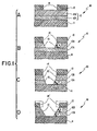
- Figs. 1A to 1D are schematic cross sectional views of the effect of the "multislope" process of the present invention on the formation of a contact via-hole through a photoresist masked PSG/SiO2 composite insulating layer.
- a wide variety of plasma gases are suitable for use according to the invention; in general, they comprise at least one fluorine compound such as trifluoromethane (CHF3), tetrafluoromethane, hexafluoroethane or nitrogen trifluoride, usually in a mixture with inert gases such as helium or argon.
- Fluorine compounds of this type upon conversion to the plasma state, produce excited neutral and ionized species which react with the dielectric material, e.g. PSG or SiO2, to form volatile compounds, thereby etching away said layer and producing the desired via-holes.
- the choice of plasma gases is also made so as to achieve controlled erosion of the photoresist mask. This is generally accomplished by incorporating at least one oxidizer in the plasma gas. Oxygen is a preferred oxidizer by reason of this effectiveness and relative economy of use.
- the equipment used to conduct the experiments is the AME 8100 Reactive Ion Etcher manufactured by Applied Materials.
- CHF3/O2 ratio was the main parameter adjusted to obtain different slopes.
- the etch rate ratio between the resist mask and oxide layers have been continuously varied along the three steps of the method. Influence of O2 ratio in the etching process to define tapered via-hole in the insulating layer formed by a single dielectric material is admittedly known.
- CH3F is used alone in RIE equipment, it provides holes with vertical walls.
- O2 aims to obtain a sloped profile in the sidewalls of via-holes.
- this underlying insulating layer of SiO2 may constitute the gate oxide or the field oxide of a MOSFET transistor.
- Typical thicknesses are respectively 300 nm and 600 nm.
- a thick photoresist layer 13 (thickness about 1200 nm) is applied thereon, exposed and developed by standard techniques, so as to form a photoresist mask provided with an opening 14 and to expose a portion of the top PSG layer 12.
- the exposure and development are performed in the normal way, so that the edges of the photoresit mask are substantially vertical, say in the 80-85 deg. range.
- the photoresit layer 13 may also be cured to provide a tapered sidewall opening as well.
- any kind of known photoresists such as AZ 1350 J manufactured by Shipley Inc. may be used. It is an important aspect of the method of the present invention to be photoresist independent.
- the first step consists in plasma etching the PSG layer 12B with an O2 flow of 15% of the total gas flow to produce an opening 15 with a tapered slope in the top PSG layer 12B.
- This step ends when the SiO2 underlayer 12A, used as an etch stop layer, is reached.
- the degree of taper A is about 65 deg.
- the etch parameters of step 1 are:
- the key parameter is of course the CHF3/O2 ratio which has to be about six; in others words the proportion of O2 is abo ut 15% of the mixture. All others parameters are less determinant and may vary to some extent.
- the pressure is normally maintained lower than 50 mTORR, e.g. in the range of about 10-30 mTORR. So the "multislope" process of the present invention operates with unusually high pressure.
- the second step with the standard SiO2 etch process conditions is used for the transfer of the previous degree of taper A in the bottom SiO2 layer 12A.
- This step preferably ends approximately 100 nm before the polysilicon land 11 is exposed (not represented).
- the structure of Fig. 1B is contacted with a plasma under etching conditions.
- the etch parameters of step 2 are:
- CHF3 is a polymerizing gas, using it causes polymer deposition.
- the role of O2 is to ash the polymers. It is known that SiO2 etches slowly compared to PSG. During SiO2 etching, the slope of the hole, referenced 15 ⁇ , produced in the PSG layer 12B, increases to 75 deg. or 80 deg. when uncured photoresist is used, which is not desired. This degree of taper will be corrected during step 3. During this step, the degree of taper A, has been transferred from the PSG layer to the SiO2 layer, forming hole 16 in the SiO2 underlying layer 12A. The CHF3/O2 ratio is about 28, which means that the proportion of O2 in the mixture is about 3%.
- Fig. 1C shows the resulting structure and respective tapered slopes of the openings as obtained after the second step.
- this third step is to etch fast the resist mask, without impacting the slope of the hole in the SiO2 layer 12A which is correct but significantly correcting hole sidewalls in the PSG layer 12B to reach the appropriate 60 deg. slope.
- the rate of erosion of the photoresist mask 13 varies directly with the proportion of O2 in the plasma and controls the angle at which the via-hole in the SiO2 layer is tapered.
- the etch parameters of step 3 are:
- Fig. 1D shows the resulting structure after the third step.
- the final tapered slope A of the hole 17 produced in the composite PSG/SiO2 insulating layer is about 60 deg. (in the 55/65 deg. range).
- reference 14 ⁇ shows the final opening in said photoresist mask.
- This method is able to achieve slopes from 50 to 60 deg. or 60 to 70 deg. depending wether the photoresist has been cured or not.
- This degree of taper is good enough for a continuous metal film coverage over the edge (no edge breaks). It is to be noted too, that the final structure exhibits approximately the same degree of taper for both the top and bottom insulating layers although they have significantly different etch rates.
- a last, a CF4 cleaning step is used to achieve good contact resistance and remove contaminants.
- step 4 The clean parameters of step 4 are:
- the desired slope profile is achieved in three steps according to the following recommendations:
- the etch rate of the top insulating layer to be etched and the mask erosion must be ajusted at a given etch rate ratio depending on the materials used.
- the partial pressure is tuned to get a horizontal component of the etching. This first etching step ends when the bottom insulating layer is reached.
- a vertical etching with high selectivity with the mask is necessary to transfer the slope of the top layer into the underlying bottom one. This second etch ends a few thousand Angstroems before the active substrate material.
- the last etching step aims to rebuilt the previous tapered slope in the top layer. This is done by etching faster the mask than the insulating layer. In this step, the top layer is etched faster than the bottom one. It allows the few remaining Angstroems to be removed before the end-etch.
- the above method has been described with reference to a composite insulating layer comprised of two insulating layers: a top PSG layer overlying a bottom SiO2 layer with the etching rate of the PSG material higher than the etching rate of the SiO2 material.
- the method may be generalized to even further others situations such as different slopes, different materials, etc...
- the desired slope profile is achieved by using the same CHF3/O2 ratio and the etch rate ratio is given below depending the value of the desired slope:
- the desired slope profile is still achieved in three steps according to the following recommendations:
- the CHF3/O2 ratio must still be adjusted to get the desired slope in the top insulating layer.
- the CHF3/O2 ratio has to be adjusted to control the etch rate ratio between the mask and insulating layers.
- a three step process is still appropriate whatever the respective etch rates of the top and bottom insulating layers.
Landscapes
- Drying Of Semiconductors (AREA)
- Internal Circuitry In Semiconductor Integrated Circuit Devices (AREA)
Priority Applications (4)
| Application Number | Priority Date | Filing Date | Title |
|---|---|---|---|
| EP86430035A EP0263220B1 (fr) | 1986-10-08 | 1986-10-08 | Procédé pour la formation d'un trou de contact à pente désirée dans une couche composée d'isolants masquée par du photorésist |
| DE8686430035T DE3686721D1 (de) | 1986-10-08 | 1986-10-08 | Verfahren zur herstellung einer kontaktoeffnung mit gewuenschter schraege in einer zusammengesetzten schicht, die mit photoresist maskiert ist. |
| JP62179271A JPH0626205B2 (ja) | 1986-10-08 | 1987-07-20 | 複合絶縁層に傾斜のついた開口を形成する方法 |
| US07/099,856 US4814041A (en) | 1986-10-08 | 1987-09-22 | Method of forming a via-hole having a desired slope in a photoresist masked composite insulating layer |
Applications Claiming Priority (1)
| Application Number | Priority Date | Filing Date | Title |
|---|---|---|---|
| EP86430035A EP0263220B1 (fr) | 1986-10-08 | 1986-10-08 | Procédé pour la formation d'un trou de contact à pente désirée dans une couche composée d'isolants masquée par du photorésist |
Publications (2)
| Publication Number | Publication Date |
|---|---|
| EP0263220A1 true EP0263220A1 (fr) | 1988-04-13 |
| EP0263220B1 EP0263220B1 (fr) | 1992-09-09 |
Family
ID=8196403
Family Applications (1)
| Application Number | Title | Priority Date | Filing Date |
|---|---|---|---|
| EP86430035A Expired EP0263220B1 (fr) | 1986-10-08 | 1986-10-08 | Procédé pour la formation d'un trou de contact à pente désirée dans une couche composée d'isolants masquée par du photorésist |
Country Status (4)
| Country | Link |
|---|---|
| US (1) | US4814041A (fr) |
| EP (1) | EP0263220B1 (fr) |
| JP (1) | JPH0626205B2 (fr) |
| DE (1) | DE3686721D1 (fr) |
Cited By (12)
| Publication number | Priority date | Publication date | Assignee | Title |
|---|---|---|---|---|
| EP0436387A3 (en) * | 1990-01-03 | 1991-10-16 | Hewlett-Packard Company | Single chamber via etch through a dual-layer dielectric |
| EP0463165A4 (en) * | 1989-09-09 | 1992-03-11 | Tadahiro Ohmi | Device and method of manufacturing the same; and semiconductor device and method of manufacturing the same |
| EP0766303A3 (fr) * | 1995-09-29 | 1997-04-23 | Toshiba Kk | |
| EP0849789A3 (fr) * | 1996-12-20 | 1999-08-18 | Texas Instruments Incorporated | Méthode de gravure d'un diélectrique multi-couche d'un IC |
| KR100425100B1 (ko) * | 2001-08-27 | 2004-03-30 | 엘지전자 주식회사 | 건식식각에 의한 그루브 제조방법 및 그를 이용한광통신용소자 |
| WO2005036625A1 (fr) * | 2003-09-12 | 2005-04-21 | International Business Machines Corporation | Techniques de modelisation de caracteristiques dans des dispositifs semi-conducteurs |
| EP1361478A4 (fr) * | 2001-02-15 | 2008-05-21 | Dainippon Printing Co Ltd | Masque a dephasage et son procede de fabrication |
| US7633085B2 (en) | 1999-03-29 | 2009-12-15 | Semiconductor Energy Laboratory Co., Ltd. | Semiconductor device and manufacturing method thereof |
| US7727898B2 (en) | 1995-11-27 | 2010-06-01 | Semiconductor Energy Laboratory Co., Ltd | Semiconductor device and method of fabricating same |
| US7786553B1 (en) | 1995-11-27 | 2010-08-31 | Semiconductor Energy Laboratory Co., Ltd. | Method of fabricating semiconductor device |
| CN101937865B (zh) * | 2009-07-03 | 2012-01-25 | 中芯国际集成电路制造(上海)有限公司 | 沟槽的形成方法 |
| CN110120382A (zh) * | 2019-05-23 | 2019-08-13 | 上海华虹宏力半导体制造有限公司 | 半导体器件及形成方法 |
Families Citing this family (69)
| Publication number | Priority date | Publication date | Assignee | Title |
|---|---|---|---|---|
| JPH0691046B2 (ja) * | 1986-11-19 | 1994-11-14 | 日本電気株式会社 | 反応性イオンエツチング方法 |
| US5234633A (en) * | 1987-12-28 | 1993-08-10 | Canon Kabushiki Kaisha | Cast molding die and process for producing information recording medium using the same |
| JP2628339B2 (ja) * | 1988-05-13 | 1997-07-09 | 日本電信電話株式会社 | 半導体装置の製造方法 |
| DE3915650A1 (de) * | 1989-05-12 | 1990-11-15 | Siemens Ag | Verfahren zur strukturierung einer auf einem halbleiterschichtaufbau angeordneten schicht |
| EP0416809A3 (en) * | 1989-09-08 | 1991-08-07 | American Telephone And Telegraph Company | Reduced size etching method for integrated circuits |
| US5068707A (en) * | 1990-05-02 | 1991-11-26 | Nec Electronics Inc. | DRAM memory cell with tapered capacitor electrodes |
| US5225376A (en) * | 1990-05-02 | 1993-07-06 | Nec Electronics, Inc. | Polysilicon taper process using spin-on glass |
| EP0469370A3 (en) * | 1990-07-31 | 1992-09-09 | Gold Star Co. Ltd | Etching process for sloped side walls |
| JP2794499B2 (ja) | 1991-03-26 | 1998-09-03 | 株式会社半導体エネルギー研究所 | 半導体装置の作製方法 |
| US5203957A (en) * | 1991-06-12 | 1993-04-20 | Taiwan Semiconductor Manufacturing Company | Contact sidewall tapering with argon sputtering |
| US5180689A (en) * | 1991-09-10 | 1993-01-19 | Taiwan Semiconductor Manufacturing Company | Tapered opening sidewall with multi-step etching process |
| US5217567A (en) * | 1992-02-27 | 1993-06-08 | International Business Machines Corporation | Selective etching process for boron nitride films |
| US5269880A (en) * | 1992-04-03 | 1993-12-14 | Northern Telecom Limited | Tapering sidewalls of via holes |
| US5175127A (en) * | 1992-06-02 | 1992-12-29 | Micron Technology, Inc. | Self-aligned interlayer contact process using a plasma etch of photoresist |
| US5549784A (en) * | 1992-09-04 | 1996-08-27 | Intel Corporation | Method for etching silicon oxide films in a reactive ion etch system to prevent gate oxide damage |
| US5268332A (en) * | 1992-11-12 | 1993-12-07 | At&T Bell Laboratories | Method of integrated circuit fabrication having planarized dielectrics |
| JP2787646B2 (ja) | 1992-11-27 | 1998-08-20 | 三菱電機株式会社 | 半導体装置の製造方法 |
| US5308415A (en) * | 1992-12-31 | 1994-05-03 | Chartered Semiconductor Manufacturing Pte Ltd. | Enhancing step coverage by creating a tapered profile through three dimensional resist pull back |
| KR0126801B1 (ko) * | 1993-12-22 | 1998-04-02 | 김광호 | 반도체 장치의 배선 형성방법 |
| JP3529849B2 (ja) * | 1994-05-23 | 2004-05-24 | 富士通株式会社 | 半導体装置の製造方法 |
| US5453403A (en) * | 1994-10-24 | 1995-09-26 | Chartered Semiconductor Manufacturing Pte, Ltd. | Method of beveled contact opening formation |
| US6040247A (en) * | 1995-01-10 | 2000-03-21 | Lg Semicon Co., Ltd. | Method for etching contact |
| KR0154702B1 (ko) * | 1995-06-09 | 1998-10-15 | 김광호 | 항복전압을 향상시킨 다이오드 제조 방법 |
| US6396078B1 (en) | 1995-06-20 | 2002-05-28 | Semiconductor Energy Laboratory Co., Ltd. | Semiconductor device with a tapered hole formed using multiple layers with different etching rates |
| KR0179791B1 (ko) * | 1995-12-27 | 1999-03-20 | 문정환 | 플래쉬 메모리 소자 및 그 제조방법 |
| KR0179792B1 (ko) * | 1995-12-27 | 1999-04-15 | 문정환 | 고밀도 플라즈마 식각장비를 이용한 슬로프 콘택 홀 형성방법 |
| US5661083A (en) * | 1996-01-30 | 1997-08-26 | Integrated Device Technology, Inc. | Method for via formation with reduced contact resistance |
| JPH09289250A (ja) * | 1996-04-24 | 1997-11-04 | Nec Corp | 半導体装置の製造方法 |
| US5652172A (en) * | 1996-04-29 | 1997-07-29 | Taiwan Semiconductor Manufacturing Company Ltd. | Method for controlling the etch profile of an aperture formed through a multi-layer insulator layer |
| US5750441A (en) | 1996-05-20 | 1998-05-12 | Micron Technology, Inc. | Mask having a tapered profile used during the formation of a semiconductor device |
| US6084305A (en) * | 1997-10-06 | 2000-07-04 | Vlsi Technology, Inc. | Shaped etch-front for self-aligned contact |
| US6143649A (en) | 1998-02-05 | 2000-11-07 | Micron Technology, Inc. | Method for making semiconductor devices having gradual slope contacts |
| TW421849B (en) * | 1998-02-23 | 2001-02-11 | Winbond Electronics Corp | Structure of multi-layered dielectric opening and its fabricating method |
| US6074957A (en) | 1998-02-26 | 2000-06-13 | Micron Technology, Inc. | Methods of forming openings and methods of controlling the degree of taper of openings |
| US6287751B2 (en) * | 1998-05-12 | 2001-09-11 | United Microelectronics Corp. | Method of fabricating contact window |
| US6326307B1 (en) * | 1999-11-15 | 2001-12-04 | Appllied Materials, Inc. | Plasma pretreatment of photoresist in an oxide etch process |
| KR20030050845A (ko) * | 2001-12-19 | 2003-06-25 | 주식회사 하이닉스반도체 | 반도체 소자의 제조방법 |
| ITMI20020931A1 (it) * | 2002-05-02 | 2003-11-03 | St Microelectronics Srl | Metodo per fabbricare circuiti elettronici integrati su un substrato semiconduttore |
| US6858542B2 (en) * | 2003-01-17 | 2005-02-22 | Freescale Semiconductor, Inc. | Semiconductor fabrication method for making small features |
| US7238609B2 (en) * | 2003-02-26 | 2007-07-03 | Matsushita Electric Industrial Co., Ltd. | Method for fabricating semiconductor device |
| US7060624B2 (en) * | 2003-08-13 | 2006-06-13 | International Business Machines Corporation | Deep filled vias |
| US7390740B2 (en) | 2004-09-02 | 2008-06-24 | Micron Technology, Inc. | Sloped vias in a substrate, spring-like contacts, and methods of making |
| US20060086690A1 (en) * | 2004-10-21 | 2006-04-27 | Ming-Huan Tsai | Dielectric etching method to prevent photoresist damage and bird's beak |
| DE102004052611A1 (de) * | 2004-10-29 | 2006-05-04 | Infineon Technologies Ag | Verfahren zur Herstellung einer mit einem Füllmaterial mindestens teilweise gefüllten Öffnung, Verfahren zur Herstellung einer Speicherzelle und Speicherzelle |
| JP2007266030A (ja) * | 2006-03-27 | 2007-10-11 | Seiko Epson Corp | 半導体装置の製造方法および半導体装置 |
| US8685861B2 (en) * | 2006-08-02 | 2014-04-01 | Globalfoundries Singapore Pte. Ltd. | Integrated circuit system with contact distribution film |
| US20080070411A1 (en) * | 2006-09-20 | 2008-03-20 | John Ghekiere | Methods for uniformly etching films on a semiconductor wafer |
| US7973413B2 (en) * | 2007-08-24 | 2011-07-05 | Taiwan Semiconductor Manufacturing Company, Ltd. | Through-substrate via for semiconductor device |
| JP5326404B2 (ja) * | 2008-07-29 | 2013-10-30 | 富士通株式会社 | モールドの製造方法 |
| US7998869B2 (en) * | 2008-10-31 | 2011-08-16 | Samsung Electronics Co., Ltd. | Contact patterning method with transition etch feedback |
| JP5446388B2 (ja) * | 2009-03-31 | 2014-03-19 | サンケン電気株式会社 | 集積化半導体装置の製造方法 |
| US8610283B2 (en) | 2009-10-05 | 2013-12-17 | International Business Machines Corporation | Semiconductor device having a copper plug |
| US8703619B2 (en) * | 2012-01-19 | 2014-04-22 | Headway Technologies, Inc. | Taper-etching method and method of manufacturing near-field light generator |
| CN102610496B (zh) * | 2012-03-31 | 2017-11-07 | 上海集成电路研发中心有限公司 | 大高宽比结构的去胶方法 |
| JP2014013810A (ja) * | 2012-07-04 | 2014-01-23 | Seiko Epson Corp | 基板、基板の製造方法、半導体装置、及び電子機器 |
| CN103779271B (zh) * | 2012-10-26 | 2017-04-05 | 中微半导体设备(上海)有限公司 | 一种倒锥形轮廓刻蚀方法 |
| CN103811408B (zh) * | 2012-11-08 | 2016-08-17 | 中微半导体设备(上海)有限公司 | 一种深硅通孔刻蚀方法 |
| US9159581B2 (en) * | 2012-11-27 | 2015-10-13 | Taiwan Semiconductor Manufacturing Company, Ltd. | Method of making a semiconductor device using a bottom antireflective coating (BARC) layer |
| US9159580B2 (en) | 2012-12-14 | 2015-10-13 | Taiwan Semiconductor Manufacturing Company, Ltd. | Method of making a semiconductor device using multiple layer sets |
| TWI513993B (zh) | 2013-03-26 | 2015-12-21 | Ind Tech Res Inst | 三軸磁場感測器、製作磁場感測結構的方法與磁場感測電路 |
| EP2819162B1 (fr) | 2013-06-24 | 2020-06-17 | IMEC vzw | Procédé de production de zones de contact sur un substrat semi-conducteur |
| CN104600027B (zh) * | 2015-01-30 | 2017-10-27 | 华进半导体封装先导技术研发中心有限公司 | 一种tsv通孔的制备工艺 |
| US9917027B2 (en) * | 2015-12-30 | 2018-03-13 | Globalfoundries Singapore Pte. Ltd. | Integrated circuits with aluminum via structures and methods for fabricating the same |
| CN105552091A (zh) * | 2016-03-09 | 2016-05-04 | 京东方科技集团股份有限公司 | 阵列基板及其制备方法、显示面板 |
| CN106946769B (zh) * | 2017-04-16 | 2019-04-02 | 内蒙古佳瑞米精细化工有限公司 | 一种2-氟-5-三氟甲基吡啶的合成方法 |
| US10157773B1 (en) * | 2017-11-28 | 2018-12-18 | Taiwan Semiconductor Manufacturing Co., Ltd. | Semiconductor structure having layer with re-entrant profile and method of forming the same |
| US10867842B2 (en) * | 2018-10-31 | 2020-12-15 | Taiwan Semiconductor Manufacturing Company, Ltd. | Method for shrinking openings in forming integrated circuits |
| CN111508835A (zh) * | 2020-04-26 | 2020-08-07 | 深圳市昭矽微电子科技有限公司 | 图形结构及其形成方法 |
| CN112928069B (zh) * | 2021-02-05 | 2023-02-28 | 长鑫存储技术有限公司 | 半导体结构的制作方法及半导体结构 |
Citations (3)
| Publication number | Priority date | Publication date | Assignee | Title |
|---|---|---|---|---|
| US3880684A (en) * | 1973-08-03 | 1975-04-29 | Mitsubishi Electric Corp | Process for preparing semiconductor |
| US4376672A (en) * | 1981-10-26 | 1983-03-15 | Applied Materials, Inc. | Materials and methods for plasma etching of oxides and nitrides of silicon |
| US4484979A (en) * | 1984-04-16 | 1984-11-27 | At&T Bell Laboratories | Two-step anisotropic etching process for patterning a layer without penetrating through an underlying thinner layer |
Family Cites Families (8)
| Publication number | Priority date | Publication date | Assignee | Title |
|---|---|---|---|---|
| JPS57100731A (en) * | 1980-12-15 | 1982-06-23 | Nec Corp | Manufacture of semiconductor device |
| US4461672A (en) * | 1982-11-18 | 1984-07-24 | Texas Instruments, Inc. | Process for etching tapered vias in silicon dioxide |
| US4487652A (en) * | 1984-03-30 | 1984-12-11 | Motorola, Inc. | Slope etch of polyimide |
| US4522681A (en) * | 1984-04-23 | 1985-06-11 | General Electric Company | Method for tapered dry etching |
| US4631248A (en) * | 1985-06-21 | 1986-12-23 | Lsi Logic Corporation | Method for forming an electrical contact in an integrated circuit |
| JPS6218054A (ja) * | 1985-07-17 | 1987-01-27 | Hitachi Ltd | 半導体装置の製造方法 |
| US4676869A (en) * | 1986-09-04 | 1987-06-30 | American Telephone And Telegraph Company At&T Bell Laboratories | Integrated circuits having stepped dielectric regions |
| JP3131058B2 (ja) * | 1992-12-25 | 2001-01-31 | 京セラ株式会社 | アルミナ質焼結体 |
-
1986
- 1986-10-08 DE DE8686430035T patent/DE3686721D1/de not_active Expired - Lifetime
- 1986-10-08 EP EP86430035A patent/EP0263220B1/fr not_active Expired
-
1987
- 1987-07-20 JP JP62179271A patent/JPH0626205B2/ja not_active Expired - Lifetime
- 1987-09-22 US US07/099,856 patent/US4814041A/en not_active Expired - Fee Related
Patent Citations (3)
| Publication number | Priority date | Publication date | Assignee | Title |
|---|---|---|---|---|
| US3880684A (en) * | 1973-08-03 | 1975-04-29 | Mitsubishi Electric Corp | Process for preparing semiconductor |
| US4376672A (en) * | 1981-10-26 | 1983-03-15 | Applied Materials, Inc. | Materials and methods for plasma etching of oxides and nitrides of silicon |
| US4484979A (en) * | 1984-04-16 | 1984-11-27 | At&T Bell Laboratories | Two-step anisotropic etching process for patterning a layer without penetrating through an underlying thinner layer |
Non-Patent Citations (5)
| Title |
|---|
| EXTENDED ABSTRACTS OF THE JOURNAL OF THE ELECTROCHEMICAL SOCIETY, vol. 83-1, May 1983, pages 261-262, no. 163, Pennington, New Jersey, US; E.CRABBE et al.: "Tapering CVD SIO2 vias for improved metal step coverage using RIE" * |
| EXTENDED ABSTRACTS OF THE JOURNAL OF THE ELECTROCHEMICAL SOCIETY, vol. 83-1, May 1983, pages 265-266, no. 165, Pennington, New Jersey, US; M.T.DUFFY et al.: "Dry etching of dielectrics for VLSI application" * |
| IBM TECHNICAL DISCLOSURE BULLETIN, vol. 24, no. 9, February 1982, pages 4728-4729, New York, US; H.M.DALAL et al.: "Methods of opening contact holes in oxide-nitride structure" * |
| SOLID STATE TECHNOLOGY, vol. 27, no. 4, April 1984, pages 177-183, Port Washington, New York, US; D.HG.CHOE et al.: "Production RIE - I. Selective dielectric etching" * |
| SOLID-STATE TECHNOLOGY, vol. 25, no. 8, August 1982, pages 88-92, Port Washington, New York, US; C.MULLINS: "Single wafer plasma etching" * |
Cited By (18)
| Publication number | Priority date | Publication date | Assignee | Title |
|---|---|---|---|---|
| EP0463165A4 (en) * | 1989-09-09 | 1992-03-11 | Tadahiro Ohmi | Device and method of manufacturing the same; and semiconductor device and method of manufacturing the same |
| US5854097A (en) * | 1989-09-09 | 1998-12-29 | Canon Kabushiki Kaisha | Method of manufacturing a semiconductor device |
| EP0436387A3 (en) * | 1990-01-03 | 1991-10-16 | Hewlett-Packard Company | Single chamber via etch through a dual-layer dielectric |
| EP0766303A3 (fr) * | 1995-09-29 | 1997-04-23 | Toshiba Kk | |
| US5976972A (en) * | 1995-09-29 | 1999-11-02 | Kabushiki Kaisha Toshiba | Method of making semiconductor apparatus having wiring groove and contact hole formed in a self-alignment manner |
| US6163067A (en) * | 1995-09-29 | 2000-12-19 | Kabushiki Kaisha Toshiba | Semiconductor apparatus having wiring groove and contact hole in self-alignment manner |
| US7727898B2 (en) | 1995-11-27 | 2010-06-01 | Semiconductor Energy Laboratory Co., Ltd | Semiconductor device and method of fabricating same |
| US8283788B2 (en) | 1995-11-27 | 2012-10-09 | Semiconductor Energy Laboratory Co., Ltd. | Method of fabricating semiconductor device |
| US7800235B2 (en) | 1995-11-27 | 2010-09-21 | Semiconductor Energy Laboratory Co., Ltd. | Method of fabricating semiconductor device |
| US7786553B1 (en) | 1995-11-27 | 2010-08-31 | Semiconductor Energy Laboratory Co., Ltd. | Method of fabricating semiconductor device |
| EP0849789A3 (fr) * | 1996-12-20 | 1999-08-18 | Texas Instruments Incorporated | Méthode de gravure d'un diélectrique multi-couche d'un IC |
| US7633085B2 (en) | 1999-03-29 | 2009-12-15 | Semiconductor Energy Laboratory Co., Ltd. | Semiconductor device and manufacturing method thereof |
| US8093591B2 (en) | 1999-03-29 | 2012-01-10 | Semiconductor Energy Laboratory Co., Ltd. | Semiconductor device and manufacturing method thereof |
| EP1361478A4 (fr) * | 2001-02-15 | 2008-05-21 | Dainippon Printing Co Ltd | Masque a dephasage et son procede de fabrication |
| KR100425100B1 (ko) * | 2001-08-27 | 2004-03-30 | 엘지전자 주식회사 | 건식식각에 의한 그루브 제조방법 및 그를 이용한광통신용소자 |
| WO2005036625A1 (fr) * | 2003-09-12 | 2005-04-21 | International Business Machines Corporation | Techniques de modelisation de caracteristiques dans des dispositifs semi-conducteurs |
| CN101937865B (zh) * | 2009-07-03 | 2012-01-25 | 中芯国际集成电路制造(上海)有限公司 | 沟槽的形成方法 |
| CN110120382A (zh) * | 2019-05-23 | 2019-08-13 | 上海华虹宏力半导体制造有限公司 | 半导体器件及形成方法 |
Also Published As
| Publication number | Publication date |
|---|---|
| JPH0626205B2 (ja) | 1994-04-06 |
| US4814041A (en) | 1989-03-21 |
| EP0263220B1 (fr) | 1992-09-09 |
| JPS63104338A (ja) | 1988-05-09 |
| DE3686721D1 (de) | 1992-10-15 |
Similar Documents
| Publication | Publication Date | Title |
|---|---|---|
| EP0263220B1 (fr) | Procédé pour la formation d'un trou de contact à pente désirée dans une couche composée d'isolants masquée par du photorésist | |
| US4522681A (en) | Method for tapered dry etching | |
| US4495220A (en) | Polyimide inter-metal dielectric process | |
| US6362111B1 (en) | Tunable gate linewidth reduction process | |
| US8343868B2 (en) | Device and methodology for reducing effective dielectric constant in semiconductor devices | |
| US8093155B2 (en) | Method of controlling striations and CD loss in contact oxide etch | |
| US6010829A (en) | Polysilicon linewidth reduction using a BARC-poly etch process | |
| US5691246A (en) | In situ etch process for insulating and conductive materials | |
| US4824521A (en) | Planarization of metal pillars on uneven substrates | |
| JPH0519977B2 (fr) | ||
| JPH0573338B2 (fr) | ||
| EP0536968A2 (fr) | Procédé de formation de trous de contact pendant la fabrication de composants semi-conducteurs | |
| KR20010098774A (ko) | 반도체 장치와 그 제조 방법 | |
| US6211557B1 (en) | Contact structure using taper contact etching and polycide step | |
| JPH1197414A (ja) | 酸化シリコン系絶縁膜のプラズマエッチング方法 | |
| US6303489B1 (en) | Spacer - defined dual damascene process method | |
| JP2650313B2 (ja) | ドライエッチング方法 | |
| US6579792B2 (en) | Method of manufacturing a semiconductor device | |
| JP3460436B2 (ja) | 半導体装置の製造方法 | |
| KR930008841B1 (ko) | 반도체 제조중 콘택트홀의 형성방법 | |
| KR100668726B1 (ko) | 반도체 소자의 비트라인 콘택 형성방법 | |
| KR100365767B1 (ko) | 반도체장치의콘택홀형성방법 | |
| JPH0729886A (ja) | 半導体装置のコンタクトホール形成方法 | |
| KR19980025508A (ko) | 반도체 소자의 콘택홀 형성 방법 | |
| KR20020050517A (ko) | 반도체 소자의 콘택홀 형성 방법 |
Legal Events
| Date | Code | Title | Description |
|---|---|---|---|
| PUAI | Public reference made under article 153(3) epc to a published international application that has entered the european phase |
Free format text: ORIGINAL CODE: 0009012 |
|
| AK | Designated contracting states |
Kind code of ref document: A1 Designated state(s): DE FR GB |
|
| 17P | Request for examination filed |
Effective date: 19880823 |
|
| 17Q | First examination report despatched |
Effective date: 19910320 |
|
| GRAA | (expected) grant |
Free format text: ORIGINAL CODE: 0009210 |
|
| AK | Designated contracting states |
Kind code of ref document: B1 Designated state(s): DE FR GB |
|
| PG25 | Lapsed in a contracting state [announced via postgrant information from national office to epo] |
Ref country code: DE Effective date: 19920909 |
|
| PGFP | Annual fee paid to national office [announced via postgrant information from national office to epo] |
Ref country code: FR Payment date: 19920928 Year of fee payment: 7 |
|
| REF | Corresponds to: |
Ref document number: 3686721 Country of ref document: DE Date of ref document: 19921015 |
|
| ET | Fr: translation filed | ||
| PG25 | Lapsed in a contracting state [announced via postgrant information from national office to epo] |
Ref country code: GB Effective date: 19921209 |
|
| PLBE | No opposition filed within time limit |
Free format text: ORIGINAL CODE: 0009261 |
|
| STAA | Information on the status of an ep patent application or granted ep patent |
Free format text: STATUS: NO OPPOSITION FILED WITHIN TIME LIMIT |
|
| GBPC | Gb: european patent ceased through non-payment of renewal fee |
Effective date: 19921209 |
|
| 26N | No opposition filed | ||
| PG25 | Lapsed in a contracting state [announced via postgrant information from national office to epo] |
Ref country code: FR Effective date: 19940630 |
|
| REG | Reference to a national code |
Ref country code: FR Ref legal event code: ST |