EP0263275A2 - Farbtabelle - Google Patents
Farbtabelle Download PDFInfo
- Publication number
- EP0263275A2 EP0263275A2 EP87112092A EP87112092A EP0263275A2 EP 0263275 A2 EP0263275 A2 EP 0263275A2 EP 87112092 A EP87112092 A EP 87112092A EP 87112092 A EP87112092 A EP 87112092A EP 0263275 A2 EP0263275 A2 EP 0263275A2
- Authority
- EP
- European Patent Office
- Prior art keywords
- memory
- output
- lines
- look
- input
- Prior art date
- Legal status (The legal status is an assumption and is not a legal conclusion. Google has not performed a legal analysis and makes no representation as to the accuracy of the status listed.)
- Withdrawn
Links
Images
Classifications
-
- G—PHYSICS
- G09—EDUCATION; CRYPTOGRAPHY; DISPLAY; ADVERTISING; SEALS
- G09G—ARRANGEMENTS OR CIRCUITS FOR CONTROL OF INDICATING DEVICES USING STATIC MEANS TO PRESENT VARIABLE INFORMATION
- G09G5/00—Control arrangements or circuits for visual indicators common to cathode-ray tube indicators and other visual indicators
- G09G5/02—Control arrangements or circuits for visual indicators common to cathode-ray tube indicators and other visual indicators characterised by the way in which colour is displayed
- G09G5/06—Control arrangements or circuits for visual indicators common to cathode-ray tube indicators and other visual indicators characterised by the way in which colour is displayed using colour palettes, e.g. look-up tables
Definitions
- the present invention relates to a look-up table and, more particularly, a look-up table for interfacing the output of a frame buffer memory with a color monitor in a digital, color graphics display system.
- look-up tables for interfacing the output of a memory frame buffer with a color monitor in a digital, color graphics display system are well-known in the art.
- look-up tables are merely buffered memories which control the display of color on the color display apparatus. They are used to alter instantly and dynamically the color, brightness and contrast of the displayed image, while the stored image data in the frame buffer remains unaltered.
- a look up table comprising a table of random entries.
- a table of random entries has stored therein every possible combination of inputs mapped to a unique output. Thus, all the input lines are addresses to a memory location and the output is the data stored in that memory location.
- a look-up table comprised of a memory size 216 ⁇ 16 or 128k RAM bytes is needed. Such a look-up table is adequate for low number of bits from the frame buffer memory.
- a look-up table for interfacing the output of a memory frame buffer with a color monitor in a digital, color graphics display apparatus.
- the table has means for duplicating some of the outputs of the memory frame buffer.
- a first memory means receives the output and the duplicated output as addresses therefor. The first memory means generates a first output from the address that is received.
- a second memory means receives the first output as address therefor and generates a second output from the address received.
- a third memory means receives the second output as address therefor and generates a third output from the address received and supplies the third output to the color monitor.
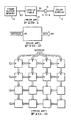
- a look-up table 10 receives the output of a frame buffer memory 12 as addresses for the table 10.
- the data at the address supplied from the frame buffer memory 12 is then outputted from the table 10 to a D-to-A converter 14, which is then passed to a color display 16.
- the look-up table is used, among others, to alter the color, brightness and contrast of the image being displayed on the color display 16, while the image stored in the frame buffer memory 12 remains unaltered.
- the Table of Random Entries Look-Up Table comprises a single memory bank such as a RAM or ROM adapted to receive input lines and output therefrom the data at the address addressed by the input lines.
- a memory size of 16 billion bytes of storage is required.
- FIG. 3 there is shown a block diagram of a Space Rotation Look-Up Table of the prior art.
- the address lines are partitioned into a plurality of groups of input lines.
- Each of the group of input lines is the input to a plurality of memory cells.
- Each of the group of input lines addresses a memory cell.
- if 32 address lines are provided there are four groups of eight input lines.
- Each of the group of eight input lines addresses four 8 ⁇ 8 memory cell.
- the outputs of each row of 8 ⁇ 8 memory cells are then added together and form four groups of eight output lines resulting in 32 output lines.
- one of the shortcomings of this look-up table is that one group of input lines cannot affect the entire look-up table.
- FIG. 4 there is shown a schematic block diagram of a Cross-Point Switch Look-Up Table of the prior art.
- This look-up table comprises a plurality of input columns lines and a plurality of output row data lines. At the intersection of each column in each row is a switch or a memory cell which can interconnect that row with that column. By appropriate programming it can be seen that a single input line can affect all of the output data lines.
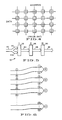
- the look-up table 10 of the present invention receives the output data from the frame buffer memory along the input lines 20 thereto. Some or all of the input lines 20 are duplicated. The input lines 20 and the duplicated input lines 20A are then supplied to a first memory bank 22. The input lines 20 and the duplicated input lines 20A form the addresses for the first memory bank 22. At the address supplied by the input lines 20 and the duplicated input lines 20A, the data is then supplied along the first output lines 24. The data on the first output lines 24 are then supplied to a second memory bank 26 as the address thereto. Data at the address, determined by the first output lines 24, are supplied from the second memory bank 26 along the second output lines 28. The second output lines 28 are then supplied to a third memory bank 30 as the input address therefor. Data at the address supplied by the second output lines 28 are then supplied by the third memory bank 30 and placed on the output lines 32, which form the output of the look-up table 10.
- the look-up table 10 of the present invention is particularly suited to receive 32 lines of data from the frame buffer memory 12 along the input lines 20.
- the 32 lines of input 20 are divided into groups of four lines within each group, designated as A, B, C...H.
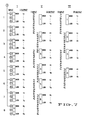
- Fig. 7 there is shown in greater schematic detail of the look-up table 10 of the present invention, wherein 32 lines of input 20 are supplied to the look-up table 10.
- the input lines 20 to the look-up table 10 are duplicated.
- all of the input lines 20 are duplicated.
- the input lines 20 and the duplicated input lines 20A are supplied to a first memory bank 22.
- the first memory bank 22 comprises 8 memory chips, with each memory chip containing 2k bytes of storage. Thus, 11 address input lines are supplied to each memory chip.
- the 8 memory chips of the first memory bank 22 are designated as 1, 2, 3...8.
- group B and group A of the input lines 20 and three other lines form the 11 lines of address input to the memory chip 1.
- group C and group B group B being duplicated
- the three other lines form the 11 address input lines to memory chip 2.
- the three other lines supplied to memory chip 2 are the same three other lines supplied to memory chip 1 and are tied together.
- LSB means least significant bit
- MSB means most significant bit.
- the three other lines are connected in common to memory chips 1 through 8 and occupy the three most significant bits of each of the memory chips.
- the lower 8 address input lines of each memory chip are taken from the groups of input lines 20.
- the 8 bits are from groups C and D.
- the groups are D and E.
- the groups are E and F.
- For memory chip 6 the groups are F and G.
- the groups are G and H.
- the groups are H and A.
- each memory chip has 2k bytes of storage with 8 lines of output. Each line of output is designated as the subscript to the chip number. Thus, the number 34 means the 5th bit of the output of memory chip 3. (The subscript 4 indicates the fifth bit because the first bit is the subscript 0.)
- the 64 lines of output (8 chips, each providing 8 lines of output from the first memory bank 22) are supplied to the second memory bank 26, along the first output lines 24.
- the second memory bank 26 comprises 6 memory chips, each also having 2k bytes of storage. These are also designated sequentially as memory chips 1, 2, ...6. Again, since each memory chip has 2k bytes of storage, 11 address input lines are needed to address each memory chip. Since there are 64 lines of output from the first memory bank 22, supplying to 66 (6 chips, each with 11 lines of input) possible input lines, two of the memory chips in the second memory bank 26 will only have 10 lines of input. The 8 output lines of each memory chip of the first memory bank 22 are interconnected as the address input lines for all of the 6 memory chips of the second memory bank 26. Thus, for example, line 10 is supplied on the input address line to memory chip 1 of the second memory bank 26.
- Line 11 of the output of memory chip 1 of the first memory bank 22 is connected to the input address line of memory chip No. 2 of the second memory bank 26.
- Line 12 is connected to memory chip 3.
- Line 13 is connected to memory chip No. 4.
- Lines 14 and 15 are connected to memory chip No. 5.
- Lines 16 and 17 are connected to memory chip No. 6.
- Input address lines for memory chip No. 1 of the second memory bank 26 are 10 26 27 34 35 43 52 61 70 84 85.
- the input address lines for memory chip No. 2 of the second memory bank 26 are 11 20 36 37 44 45 53 62 71 86 87.
- the input lines are 12 21 30 46 47 54 55 63 72 80.
- the input lines are 13 22 31 40 56 57 64 65 73 81.
- the input lines are 14 15 23 32 41 50 66 67 74 75 82.
- the input lines are 16 17 24 25 33 42 51 60 76 77 83.
- each of the memory chips of the second memory bank 26 has 8 lines of output. They are designated, using the same convention as was described for the memory chips of the first memory bank 22.
- the output of the memory chips of the second memory bank are supplied along the second output line 28 as the address input to the third memory bank 30.
- the third memory bank 30 comprises four memory chips, each memory chip having 2k bytes of storage. Again, similar to the convention described previously, each of the output lines of each of the memory chips from the second memory bank 26 is supplied as an input address to the third memory bank 30.
- the address input lines for memory chip No. 1 of the third memory bank 30 are 10 11 26 27 34 35 42 43 50 51 63.
- the address input lines for memory chip No. 2 of the third memory bank 30 are 12 13 20 21 36 37 44 45 52 53 60.
- the address input lines for memory chip No. 3 are 14 15 22 23 30 31 46 47 54 55 61.
- the address input lines for memory chip No. 4 are 16 17 24 25 32 33 40 41 56 57 62.
- Each of the four memory chips of the third memory bank 30 has 8 lines of output.
- the total output of the third memory bank 30 is 32 lines which are then supplied along the output lines 32 to the D-to-A converter 14.
- three input lines are connected to each of the memory chips of the first memory bank 22.
- the three lines are connected to all the memory chips. There are thus 8 possible combinations.
- the 8 possible combinations form 8 complete sets for the look-up 10 for 32 bits. Each of the sets can change the display on the color display 16.
- a full look-up table 10 of the present invention for 32 bits requires the use of only 18 2k byte RAM chips.
- the theory of operation of the present invention is as follows. For a large number of input lines (such as 32), the 32 input lines are divided into a plurality of small tables. The adjacent input bits are duplicated because adjacent bits are most likely to have similar meaning. Further, the outputs of the first memory bank 22 are mixed and provided as inputs to the second memory bank 26 to ensure that a single input to the first memory bank 22 can effect all of the second memory bank 26.
- the look-up table 10 of the present invention is that the input data path received by the look-up table 10 is initially and temporarily increased. Thus, the input data lines 20 are duplicated. While one embodiment has been described in which all of the input data lines 20 are duplicated, it is believed that the duplication of all of the input data lines is not necessary. Although the duplication of all of the input data lines 20 has resulted in a full look-up table for 32 bits, it is believed that the invention can be practiced equally well in which only some of the input data lines 20 are duplicated.
- the look-up table 10 of the present invention can perform functions such as change color, implement large number of overlay planes, and intelligent allocation of bit planes to windows.
Landscapes
- Engineering & Computer Science (AREA)
- Physics & Mathematics (AREA)
- Computer Hardware Design (AREA)
- General Physics & Mathematics (AREA)
- Theoretical Computer Science (AREA)
- Controls And Circuits For Display Device (AREA)
- Digital Computer Display Output (AREA)
Applications Claiming Priority (2)
| Application Number | Priority Date | Filing Date | Title |
|---|---|---|---|
| US06/912,990 US4835527A (en) | 1986-09-29 | 1986-09-29 | Look-up table |
| US912990 | 1986-09-29 |
Publications (2)
| Publication Number | Publication Date |
|---|---|
| EP0263275A2 true EP0263275A2 (de) | 1988-04-13 |
| EP0263275A3 EP0263275A3 (de) | 1990-01-10 |
Family
ID=25432817
Family Applications (1)
| Application Number | Title | Priority Date | Filing Date |
|---|---|---|---|
| EP87112092A Withdrawn EP0263275A3 (de) | 1986-09-29 | 1987-08-20 | Farbtabelle |
Country Status (5)
| Country | Link |
|---|---|
| US (1) | US4835527A (de) |
| EP (1) | EP0263275A3 (de) |
| JP (1) | JPS6472197A (de) |
| AU (1) | AU7903387A (de) |
| NZ (1) | NZ221457A (de) |
Families Citing this family (5)
| Publication number | Priority date | Publication date | Assignee | Title |
|---|---|---|---|---|
| GB8730363D0 (en) * | 1987-12-31 | 1988-08-24 | British Aerospace | Digital signal processing device |
| US5038300A (en) * | 1988-06-29 | 1991-08-06 | Digital Equipment Corporation | Extendable-size color look-up table for computer graphics systems |
| US5083257A (en) * | 1989-04-27 | 1992-01-21 | Motorola, Inc. | Bit plane partitioning for graphic displays |
| US5065149A (en) * | 1989-11-09 | 1991-11-12 | Document Technologies, Inc. | Scanned document image resolution enhancement |
| JP2583003B2 (ja) * | 1992-09-11 | 1997-02-19 | インターナショナル・ビジネス・マシーンズ・コーポレイション | グラフィックス表示システムにおけるイメージ表示方法、フレーム・バッファ及びグラフィックス表示システム |
Family Cites Families (9)
| Publication number | Priority date | Publication date | Assignee | Title |
|---|---|---|---|---|
| GB1233290A (de) * | 1969-10-02 | 1971-05-26 | ||
| GB1572318A (en) * | 1978-03-31 | 1980-07-30 | Ibm | Display system |
| EP0090596B1 (de) * | 1982-03-30 | 1986-06-25 | Crosfield Electronics Limited | Systeme zur Korrektur von Bildsignalen |
| US4591842A (en) * | 1983-05-26 | 1986-05-27 | Honeywell Inc. | Apparatus for controlling the background and foreground colors displayed by raster graphic system |
| GB2141607A (en) * | 1983-06-15 | 1984-12-19 | Philips Electronic Associated | Video display system with index pages |
| US4574277A (en) * | 1983-08-30 | 1986-03-04 | Zenith Radio Corporation | Selective page disable for a video display |
| US4673929A (en) * | 1984-04-16 | 1987-06-16 | Gould Inc. | Circuit for processing digital image data in a high resolution raster display system |
| US4745407A (en) * | 1985-10-30 | 1988-05-17 | Sun Microsystems, Inc. | Memory organization apparatus and method |
| US4942474A (en) * | 1987-12-11 | 1990-07-17 | Hitachi, Ltd. | Solid-state imaging device having photo-electric conversion elements and other circuit elements arranged to provide improved photo-sensitivity |
-
1986
- 1986-09-29 US US06/912,990 patent/US4835527A/en not_active Expired - Fee Related
-
1987
- 1987-08-14 NZ NZ221457A patent/NZ221457A/xx unknown
- 1987-08-20 EP EP87112092A patent/EP0263275A3/de not_active Withdrawn
- 1987-09-03 JP JP62219292A patent/JPS6472197A/ja active Pending
- 1987-09-28 AU AU79033/87A patent/AU7903387A/en not_active Abandoned
Also Published As
| Publication number | Publication date |
|---|---|
| AU7903387A (en) | 1988-03-31 |
| JPS6472197A (en) | 1989-03-17 |
| NZ221457A (en) | 1989-08-29 |
| EP0263275A3 (de) | 1990-01-10 |
| US4835527A (en) | 1989-05-30 |
Similar Documents
| Publication | Publication Date | Title |
|---|---|---|
| US4523276A (en) | Input/output control device with memory device for storing variable-length data and method of controlling thereof | |
| WO1990002991A1 (en) | Graphics processor with staggered memory timing | |
| JPH0420191B2 (de) | ||
| KR910013266A (ko) | 반도체 메모리 어레이의 구성방법 | |
| US4580135A (en) | Raster scan display system | |
| JPH08896U (ja) | メモリ装置 | |
| KR950015399A (ko) | 비트 단위 데이타의 입력 및 출력용 반도체 메모리 장치 | |
| KR880008323A (ko) | 바운더리-프리 반도체 메모리 장치 | |
| KR980004968A (ko) | 반도체 메모리 소자의 뱅크 분산 방법 | |
| US4845678A (en) | Memory comprising simultaneously addressable memory elements | |
| EP0263275A2 (de) | Farbtabelle | |
| US5487155A (en) | Data switch with multiplexers for forming data connections and control unit for checking permissibility of connections | |
| KR920015374A (ko) | 반도체 기억장치 | |
| EP0085480A2 (de) | Video-Anzeigesysteme | |
| JPH0191526A (ja) | プログラマブル論理素子 | |
| US5117492A (en) | Memory addressing system using first and second address signals and modifying second address responsive predetermined values of first address signal | |
| EP0145320A2 (de) | Multiplexverfahren für einen Speicherdatenbus | |
| KR900003884A (ko) | 대규모 반도체 집적회로 장치 | |
| JPH06167958A (ja) | 記憶装置 | |
| JPH0279294A (ja) | データ長変更可能メモリ | |
| CA1239700A (en) | Expandable electronic matrix | |
| SU809357A1 (ru) | Блок выборки адресов запоминающегоуСТРОйСТВА | |
| KR890017805A (ko) | 반도체 집적회로 장치 | |
| KR910004040A (ko) | 비디오신호 데이타를 기억시키는 방법 및 그 방법을 실시하기 위한 회로 | |
| KR910003527A (ko) | 비디오 그래픽 디스플레이 메모리 스위즐 논리 회로 및 방법 |
Legal Events
| Date | Code | Title | Description |
|---|---|---|---|
| PUAI | Public reference made under article 153(3) epc to a published international application that has entered the european phase |
Free format text: ORIGINAL CODE: 0009012 |
|
| 17P | Request for examination filed |
Effective date: 19870820 |
|
| AK | Designated contracting states |
Kind code of ref document: A2 Designated state(s): AT BE CH DE ES FR GB GR IT LI LU NL SE |
|
| PUAL | Search report despatched |
Free format text: ORIGINAL CODE: 0009013 |
|
| AK | Designated contracting states |
Kind code of ref document: A3 Designated state(s): AT BE CH DE ES FR GB GR IT LI LU NL SE |
|
| RAP1 | Party data changed (applicant data changed or rights of an application transferred) |
Owner name: PANSOPHIC SYSTEMS, INCORPORATED |
|
| STAA | Information on the status of an ep patent application or granted ep patent |
Free format text: STATUS: THE APPLICATION IS DEEMED TO BE WITHDRAWN |
|
| 18D | Application deemed to be withdrawn |
Effective date: 19910301 |
|
| RIN1 | Information on inventor provided before grant (corrected) |
Inventor name: HERSCH, CLIFFORD L. |