EP0263447A2 - Verfahren und Vorrichtung zur Durchführung eines Verzweigungs- und Zurück-zur-Adresse-Befehls in einem digitalen Datenverarbeitungssystem - Google Patents
Verfahren und Vorrichtung zur Durchführung eines Verzweigungs- und Zurück-zur-Adresse-Befehls in einem digitalen Datenverarbeitungssystem Download PDFInfo
- Publication number
- EP0263447A2 EP0263447A2 EP87114429A EP87114429A EP0263447A2 EP 0263447 A2 EP0263447 A2 EP 0263447A2 EP 87114429 A EP87114429 A EP 87114429A EP 87114429 A EP87114429 A EP 87114429A EP 0263447 A2 EP0263447 A2 EP 0263447A2
- Authority
- EP
- European Patent Office
- Prior art keywords
- instruction
- address
- memory
- read
- return
- Prior art date
- Legal status (The legal status is an assumption and is not a legal conclusion. Google has not performed a legal analysis and makes no representation as to the accuracy of the status listed.)
- Withdrawn
Links
Images



Classifications
-
- G—PHYSICS
- G06—COMPUTING OR CALCULATING; COUNTING
- G06F—ELECTRIC DIGITAL DATA PROCESSING
- G06F8/00—Arrangements for software engineering
- G06F8/60—Software deployment
- G06F8/65—Updates
- G06F8/66—Updates of program code stored in read-only memory [ROM]
-
- G—PHYSICS
- G06—COMPUTING OR CALCULATING; COUNTING
- G06F—ELECTRIC DIGITAL DATA PROCESSING
- G06F9/00—Arrangements for program control, e.g. control units
- G06F9/06—Arrangements for program control, e.g. control units using stored programs, i.e. using an internal store of processing equipment to receive or retain programs
- G06F9/30—Arrangements for executing machine instructions, e.g. instruction decode
- G06F9/30003—Arrangements for executing specific machine instructions
- G06F9/3005—Arrangements for executing specific machine instructions to perform operations for flow control
- G06F9/30054—Unconditional branch instructions
-
- G—PHYSICS
- G06—COMPUTING OR CALCULATING; COUNTING
- G06F—ELECTRIC DIGITAL DATA PROCESSING
- G06F9/00—Arrangements for program control, e.g. control units
- G06F9/06—Arrangements for program control, e.g. control units using stored programs, i.e. using an internal store of processing equipment to receive or retain programs
- G06F9/30—Arrangements for executing machine instructions, e.g. instruction decode
- G06F9/32—Address formation of the next instruction, e.g. by incrementing the instruction counter
- G06F9/322—Address formation of the next instruction, e.g. by incrementing the instruction counter for non-sequential address
- G06F9/323—Address formation of the next instruction, e.g. by incrementing the instruction counter for non-sequential address for indirect branch instructions
-
- G—PHYSICS
- G06—COMPUTING OR CALCULATING; COUNTING
- G06F—ELECTRIC DIGITAL DATA PROCESSING
- G06F9/00—Arrangements for program control, e.g. control units
- G06F9/06—Arrangements for program control, e.g. control units using stored programs, i.e. using an internal store of processing equipment to receive or retain programs
- G06F9/30—Arrangements for executing machine instructions, e.g. instruction decode
- G06F9/32—Address formation of the next instruction, e.g. by incrementing the instruction counter
- G06F9/322—Address formation of the next instruction, e.g. by incrementing the instruction counter for non-sequential address
- G06F9/328—Address formation of the next instruction, e.g. by incrementing the instruction counter for non-sequential address for runtime instruction patching
-
- G—PHYSICS
- G06—COMPUTING OR CALCULATING; COUNTING
- G06F—ELECTRIC DIGITAL DATA PROCESSING
- G06F9/00—Arrangements for program control, e.g. control units
- G06F9/06—Arrangements for program control, e.g. control units using stored programs, i.e. using an internal store of processing equipment to receive or retain programs
- G06F9/44—Arrangements for executing specific programs
- G06F9/448—Execution paradigms, e.g. implementations of programming paradigms
- G06F9/4482—Procedural
- G06F9/4484—Executing subprograms
- G06F9/4486—Formation of subprogram jump address
Definitions
- This invention relates to methods and apparatus for implementing branch type instructions in a digital data processing system. This invention is particularly useful in microprocessor based systems wherein some or most of the program code for controlling the microprocessor is contained in a read only memory unit.
- the typical controller architecture includes a microprocessor, a read only memory (ROM) for microprocessor instruction code storage, a read-write memory (RWM) for microprocessor work space and some amount of reserved read-write memory space for additional instruction code to be used, if needed, to "patch” (correct) ROM code "bugs" (defects) discovered after the product has been shipped to customers.
- ROM read only memory
- RWM read-write memory
- the present invention is particularly useful for minimising some of the problems associated with patching ROM code using RWM-loaded code and presents a unique solution that greatly enhances the power to do so.
- a commonly practiced method for protecting the product against this undesired event is to distribute "patch hooks" throughout key areas in the ROM code.
- a "patch hook” is a branch instruction which causes the processor to branch to the instruction patch area of the read-write memory.
- the microprocessor branches to the read-write memory space to see if an instruction routine has been loaded into that RWM space to patch or fix a ROM code problem. If it has, the microprocessor executes the RWM code and then returns back to the ROM code, usually bypassing the faulty ROM instructions. If a patch has not been loaded into the read-write memory for that patch hook, then the microprocessor simply branches back to the next sequential instruction position after its original ROM Branch instruction position and continues normal execution of ROM instructions.
- This technique allows a "patch" to be written to resolve a problem in the ROM code. This patch is then distributed on a diskette to the customers who can then download it via the appropriate software utility to the patch space in the I/O controller read-write memory. This is a much less expensive corrective method than having to manufacture and install new read only memory modules.
- a major problem with this method is that it may be necessary to duplicate large amounts of ROM code in the RWM space in order to change specific lines of code, and this in turn reduces the capability for further patching.
- Duplicating good ROM code is usually required since finding a patch hook near the faulty ROM code is a matter of change. For example, the nearest patch hook to a ROM bug may be located 500 instructions prior to the bug. In this case, it would be necessary to duplicate all 500 good instructions in the RWM patch, change the faulty ROM instructions and then branch back to the ROM code just beyond the bad code. Such a patch would probably exhaust the majority of the entire reserved RWM patch area and would greatly reduce the capability for providing additional patches.
- the system described herein provides a new processor instruction that virtually eliminates the need for duplicating the good ROM code when using an RWM patch to correct a defective segment of ROM code. This greatly increases the power of the patch hook method for correcting defects in ROM code.
- this new instruction is herein called a "Branch And Return On Address” (BAROA) instruction.
- This new instruction includes an operation code (op code) field, an entry address field and an exit address field.
- op code operation code
- this BAROA instruction is loaded into the read-write memory at the memory address to which the ROM patch hook will branch. Executing this BAROA instruction causes the processor to branch back to the ROM entry address specified by the BAROA instruction and to continue normal execution of the ROM instructions until the ROM address specified by the BAROA exit address field is reached. At this point, the processor branches back to the next consecutive read-write memory address immediately following the BAROA instruction.
- the processor then executes the corrective code which is located in the read-write memory immediately following the BAROA instruction. After the corrective code is executed, the processor branches back to and resumes execution of the ROM code, starting with the ROM instruction immediately following the ROM code segment which was replaced by the corrective code.
- this BAROA instruction eliminates the need for duplicating any good ROM code which may reside between the patch hook location and the defective code location in the read only memory.
- the first instruction of the patch routine in the read-write memory is a BAROA instruction which causes the processor to branch back and execute from the read only memory all 500 lines of ROM code separating the patch hook from the defective code segment.
- the next several instructions of the RWM patch would be the actual defect correcting code.
- the final instruction in the RWM patch is a branch back to the ROM code at a point just beyond the defective ROM code.
- the amount of RWM patch space required to correct the ROM code defect has been reduced by 500 lines of code. Since only a few lines are normally required for the defect correcting code, this represents a very substantial saving in read-write memory space.
- any single line of ROM code for example, can be deleted, altered or expanded into multiple instructions by means of a few instruction in the patch space in the read-write memory.
- a BAROA instruction To delete a line of code, only two instructions are required in the RWM patch space, namely, a BAROA instruction and a branch instruction for returning to the next line after the deleted line.
- a BAROA instruction To alter or correct a line requires only three patch space instructions, namely the BAROA instruction, the corrected instruction for the line in question and the return branch instruction.
- the BAROA and the return branch instructions are needed in addition to the instructions to be added.
- the use of the BAROA instruction considerably reduces the sizes of the patches in the read-write memory.
- the BAROA instruction also removes the burden of critically distributing patch hooks to key areas of the ROM code. Also, if used in the most efficient manner, the BAROA instruction will reduce the number of patch hooks which need to be located in the read only memory. In fact, in some cases, only a single patch hook need be placed in the read only memory.
- a method of operating a digital data processing system for enabling instructions in a read-write memory coupled to a data processor modify the code in a read only memory coupled to the data processors such method being characterised by: loading into the read-write memory a branch and return on address instruction followed by one or more other instructions for modifying the read only memory code, such branch and return on address instruction including an operation code field, a read only memory entry address field and a read only memory exit address field; commencing execution of the read only memory instructions contained in the read only memory code in a sequential manner, such read only memory instructions including a branch and return on address instruction in the read-write memory; branching to the read-write memory when such branch instruction is reached and executing the branch and return on address instruction by returning to the read only memory and executing a sequence of read only memory instructions starting with the instruction residing at the entry address provided by the branch and return on address instruction; and comparing the address of each read only memory instruction with the exit address provided by the branch and return on address instruction for returning to the read-
- branch type instructions Different names are sometimes used to refer to branch type instructions. Sometimes they are called “branch” instructions, sometimes they are called “jump” instructions and sometimes they are called “call” instructions. Other names may also be used. In each case, such an instruction may cause a processor to depart from its normal sequential execution of instructions and go to and commence executing an out of sequence set of instructions. For conditional type branch instructions, the branch may not always be taken. Unless otherwise specified, the use of the term “branch” herein and in the appended claims is intended to be generic in nature and is intended to include any and all manner of branch type instructions.
- FIG. 1 there is shown the known patch hook method of using patches in a read-write memory to correct errors and defects in the code in a read only memory.
- a portion of a random access read only memory (ROM) is indicated at 10 and a portion of a random access read-write memory (RWM) is represented at 12.
- Each memory is composed of horizontal lines of code with each line having a different memory address.
- ROM random access read only memory
- RWM random access read-write memory
- Each memory is composed of horizontal lines of code with each line having a different memory address.
- the processor executes these instructions one after the other in a sequential manner.
- the direction of execution is from the top toward the bottom of the memory portions shown in the drawings. In other words, the processor advances down the page as it moves from one instruction to the next.
- a read only memory is a memory unit or a memory element which can only be read by the processor.
- the processor cannot write to or store information into such a memory.
- the information stored in a read only memory is permanently imbedded therein at its time of manufacture.
- the processor can store or write new information into it, in addition to being able to read out from it any information previously written or stored therein.
- RAM random access read-write memory
- RWM read-write memory
- the patch hook method provides a more flexible, more economical and quicker to implement solution to the problem.
- the patch hook method is based on two underlying premises.
- the first premise is that no matter how carefully the program code is written, there is a high degree of probability that it will nevertheless contain some bugs or some deficiencies which will be discovered at a later date. Therefore, when the program code is to be imbedded in a read only memory chip, it is best to plan ahead and provide some means for taking this into account.
- the second premise is that most microprocessor based systems which use read only memories also use read-write memory chips for providing temporary work space and the like for the microprocessor. In this case, part of the read-write memory space can be reserved for use in holding code patches and code fixes for the read only memory code.
- FIG. 1 shows the known patch hook method.
- the read only memory (ROM) 10 and the read-write memory (RWM) 12 are assumed to take the form of semiconductor integrated circuit memory chips and are assumed to be coupled to a microprocessor in a microprocessor based system.
- the ROM chip 10 contains the control program for the microprocessor and, as such, contains the instructions for causing the microprocessor to perform its normal system operating functions.
- a plurality of "patch hook" instructions are included in the ROM code at points therein which appear to be strategically significant. Two such patch hooks are indicated at 13 and 14. These patch hooks 13 and 14 take the form of branch instructions.
- Branch instructions are unconditional branch type instructions which cause a branching to a specified out of sequence memory location which, in the present case, is a memory location in the read-write memory 12. These branch instructions are used with coordinating branch instructions in the RWM so that the processor branches from the ROM code to the RWM patch area and then branches back to the ROM code when no patch code has been loaded for that patch hook.
- a segment of defective ROM code is indicated at 15 in Figure 1. The remainder of the ROM memory space shown in Figure 1 is assumed to contain good and valid ROM code.
- Each patch hook instruction in ROM 10 causes an unconditional branch to its own patch hook responsive branch (back) instruction location in a patch hook branch table area 16 in the RWM 12.
- the branch (back) instruction is an unconditional branch back to the next sequential line of ROM code following the original patch hook branch instruction.
- the patch hook response instructions for patch hooks 13 and 14 are indicated at 17 and 18, respectively.
- the microprocessor commences to execute the ROM instructions one at a time in a sequential manner starting at the top of the ROM memory portion shown in Figure 1.
- the microprocessor unconditionally branches to the patch hook responsive location 17 in the read-write memory 12.
- the presence of a branch (back) instruction in this RWM location 17 indicates that there is no corrective code for the patch hook 13. In this case, the microprocessor immediately branches back to the next instruction following the patch hook instruction 13 in ROM 10.
- the microprocessor After returning to ROM 10, the microprocessor resumes the execution of the ROM instructions in a one at a time sequential manner. This continues until the next patch hook instruction 14 is reached.
- the microprocessor then unconditionally branches to the branch hook branch table area 16 in the read-write memory 12. In particular, it branches to the patch hook responsive instruction 18. In this case, there is a further branch instruction residing at the instruction location 18.
- This branch instruction 18 causes the microprocessor to branch to a patch code segment 19 located in a patch storage area of RWM 12.
- This patch code segment 19 for the patch hook 14 includes a duplicate copy 20 of the good ROM code following the patch hook 14, a corrected code segment 21 which is to replace the bad code 15 and a branch instruction 22 for branching back to the next instruction immediately following the bad code 15 in ROM 10.
- the microprocessor executes the instructions in this patch code segment 19 one at a time in a sequential manner.
- the microprocessor branches back to ROM 10 and resumes execution of the instructions in ROM 10. In this manner, the bad code 15 is bypassed by means of the patch code segment 19.
- a primary purpose of the present invention is to provide a new processor instruction for enabling patch code segments to be provided which do not require the duplication in RWM of any good and valid ROM instructions.
- the preferred format for this new instruction is shown in Figure 2.
- this new instruction is herein called a "branch and return on address” instruction. This will sometimes be referred to by the acronym of "BAROA”.
- this new instruction includes an operation code (op code) field, an entry address field and an exit address field.
- these entry and exit addresses are ROM entry and ROM exit addresses.
- FIG 3 shows the use of this new BAROA instruction for the example of Figure 1.
- the patch code segment in the read-write memory 12 is indicated at 24.
- a "branch and return on address" instruction 25 has replaced the duplicated ROM code 20 of Figure 1.
- This BAROA instruction 25 causes an immediate unconditional branch back to the read only memory 10 at the ROM entry address specified in the entry address field of the BAROA instruction.
- the address specified in the present example is the address of the next ROM instruction following the patch hook instruction 14.
- the microprocessor then resumes sequential execution of the good instructions in ROM 10 until the ROM exit address specified in the exit address field of the BAROA instruction is reached. In the present embodiment, this exit address is the address of the first ROM instruction in the bad code 15.
- the microprocessor branches back to the read-write memory 12 to the RWM instruction immediately following the BAROA instruction. The microprocessor then commences executing the corrected code 21 contained in the read-write memory 12. When the branch instruction 22 is reached, the microprocessor branches back to the read only memory 10 and resumes execution of the ROM instructions, starting with the instruction immediately following the bad code 15.
- the first instruction in the bad code 15 is not executed.
- a program counter is incremented to point to the first instruction of the bad code as the next instruction to be fetched.
- the microprocessor branches to the read-write memory 12. Thus, the first instruction of the bad code is not executed.
- the new BAROA instruction causes the microprocessor to use the read only memory for purposes of executing the good ROM instructions which are located between the patch hook and the bad code.
- the read-write memory no duplication of these good ROM instructions is required in the read-write memory.
- a savings in RWM memory space is realised. In some cases, this savings may be rather considerable and may even make the difference as to whether or not all the desired ROM code patches can be provided.
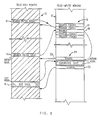
- FIG. 4 shows how a plurality of read-write memory patches can be coupled to a single patch hook instruction.
- the patch hook instruction is located at 26 and bad code segments are indicated at 27 and 28 in the read only memory.
- the patch hook instruction 26 causes a branch to a first BAROA instruction 30 located in the read-write memory.
- This BAROA instruction 30 causes a branch back to the read only memory to cause the microprocessor to execute the good ROM instructions located intermediate the patch hook 26 and the bad code 27.
- the microprocessor then branches back to the read-write memory to execute the corrected code 31 in place of the bad code 27
- BAROA Instruction 32 Immediately following the corrected code 31 is a second BAROA Instruction 32.
- This BAROA instruction 32 causes the microprocessor to branch back to the read only memory to execute the good ROM instructions residing therein intermediate the bad code 27 and the second segment of bad code 28.
- the microprocessor Immediately following execution of the good ROM instruction immediately preceding the bad code 28, the microprocessor returns to the read-write memory to execute a second segment of corrected code 33 in place of the bad code 28.
- the RWM branch instruction 34 causes a branch back to the read only memory and the microprocessor resumes executing the good ROM instructions following the bad code 28.
- this process may be repeated and additional RWM patches may be coupled to the ROM patch hook instruction 26.
- this technique may be extended so that only a single patch hook instruction is required in the read only memory. In such a case, all RWM patches would be coupled to this single ROM patch hook. This would eliminate the need for distributing a goodly number of patch hooks throughout the ROM code. It would also eliminate the need for all but one of the initial patch hook responsive branch table instructions shown at 16 in Figures 1 and 3.
- BAROA branch and return on address
- Figure 5 shows how the BAROA instruction can be used to insert additional code into a ROM program at a point where there is no bad code to be replaced.
- the appropriate patch hook instruction is indicated at 35 in the read only memory and the ROM location at which the additional code is to be inserted is indicated by the dash line 36.
- the read-write memory includes the BAROA instruction 37, the additional code 38 to be inserted and the concluding branch instruction 39.
- the exit address field of the BAROA instruction contains the address of the ROM instruction immediately following the desired insertion point 36.
- This ROM instruction is not executed at this point and the return to the read-write memory takes place immediately following execution of the ROM instruction preceding the insertion point.
- the branch address contained in the concluding RWM branch instruction 39 is the address of the ROM instruction immediately following the desired insertion point 36 and this instruction is now executed when this branch is taken.
- Figure 6 shows how the BAROA instruction may be used to effectively delete undesired ROM instructions for the case where there are no corrected instructions to take their place.
- the read only memory includes a patch hook instruction 40 and the code to be deleted is indicated at 41.
- the read-write memory includes a BAROA instruction 42 and a branch instruction 43. These two instructions 42 and 43 are sufficient for executing the intermediate good code in the read only memory and for bypassing the undesired code (deleted code) indicated at 41 in the read only memory.
- FIG. 7 shows a representative embodiment of a digital data processing system which includes a representative form of structure for practicing the present invention.
- a microprocessor based input/output (I/O) controller 44 of a type which may be used for coupling a peripheral device to a host computer.
- This I/O controller 44 includes a microprocessor 45, a random access read only memory (ROM) 46, a random access read-write memory (RWM) 47 and external interfaces 48 and 49.
- the latter four units 46 - 49 are connected to the I/O bus of the microprocessor 45.
- This microprocessor I/O bus includes a data bus 50, an address bus 51 and a control bus 52.
- the external interface 48 is connected to the peripheral device (not shown), while the external interface 49 is connected to the host computer I/O bus (not shown).
- the I/O controller 44 serves to pass information back and forth between the peripheral device and the host computer.
- the read only memory 46 contains the program instructions which control the operation of the I/O controller 44.
- the instructions stored in ROM 46 include at least one patch hook instruction for use in providing corrections to the control program contained in ROM 46.
- the read-write memory 47 includes work space for the microprocessor 45 and some reserved storage space for storing any patches that may be needed for the control program in ROM 46.
- patch code When patch code is needed in the read-write memory 47, such code is installed therein by downloading it from the host processor via the external interface 49. Typically, code patches and code fixes will be recorded onto a diskette which is distributed to the user of the data processing equipment. This diskette is inserted into the diskette unit in the host computer and the patch code is read therefrom and stored into the main storage unit in the host computer. From there, it is transferred and written into the read-write memory 47 of the I/O controller by way of the external interface 49. After storage in the RWM 47, it is ready for use by the I/O controller 44.
- the digital data processor represented by microprocessor 45 includes various instruction and data processing elements.
- One such element is a program counter 54 for holding the memory address of the instruction to be executed.
- memory address is meant the instruction address in ROM 46 or, if a patch is in progress, the memory address in RWM 47. It is assumed herein that ROM 46 and RWM 47 are assigned to two different address ranges so that there is no ambiguity as to which memory is being addressed.
- the normal non-branch procedure for the microprocessor 45 is to increment the count value in program counter 54 at some point during the execution of each instruction so as to provide therein the address of the next instruction to be fetched. At the tail end of each instruction, this address in program counter 54 is used to fetch the next instruction from ROM 46 or RWM 47, as the case may be. For the case of a branch instruction, if the branch is to be taken, then the branch address is loaded into the program counter 54 before the next instruction is fetched.
- the microprocessor 45 also includes an instruction register 55 for receiving the operation code field of the instruction to be executed.
- Microprocessor 45 fetches an instruction by taking the address in the program counter 54 and supplying it by way of an address buffer 56 and address bus 51 to the appropriate memory unit say, for example, the read only memory 46.
- ROM 46 thereafter outputs onto the data bus 50 the addressed instruction.
- This instruction is supplied by way of the data buffer 57 to the internal microprocessor bus 58.
- the operation code field of this instruction is passed by way of a multiplexer 59 and loaded into the instruction register 55. The normal operation of the multiplexer 59 is to connect the microprocessor bus 58 to the input of the instruction register 55.
- the microprocessor 45 further includes a control unit 60 responsive to the operation code in instruction register 55 for generating the elemental control signals which control the various elements with the microprocessor and the movement of instructions and data from place to place in the microprocessor.
- a clock pulse generator 61 supplies timing pulses to the control unit 60 for defining the different time states or timing intervals associated with the execution of each instruction supplied to the instruction register 55.
- the control unit 60 would include a microword generating mechanism for generating a sequence of microwords for each processor instruction resident in the instruction register 55, a control register for receiving each microword and a decoder responsive to the microword in the control register for producing the elemental control signals supplied to the remainder of the microprocessor.
- microprocessor 45 Other elements included in the microprocessor 45 are an arithmetic and logic unit (ALU) 62 and a pair of registers 63 and 64 for driving the two inputs thereof.
- ALU 62 performs arithmetic operations like adding and subtracting and logic operations like ANDing and ORing the two numerical values supplied by the registers 63 and 64.
- a further element contained in the microprocessor 45 is a register array 65 which provides various working registers which are used by the microprocessor. These registers include, for example, an address register, a stack pointer register and a plurality of general purpose registers.
- Microprocessor 45 also includes a register stack 66 for use in executing Push and Pop instructions and a stack address register 67 for addressing the register stack 66. In some data processors, the register stack 66 instead takes the form of a reserved stack area in the read-write memory 47.
- the digital data processing system of Figure 7 also includes means for suppling a branch and return on address (BAROA) instruction, such instruction having an operation code field, a memory entry address field and a memory exit address field.
- BAROA branch and return on address
- this includes the read-write memory 47, wherein the branch and return on address instructions are stored, the data bus 50, the data buffer 57 and the microprocessor bus 58.
- the data processor of Figure 7 further includes means for loading the operation code field of the branch and return on address instruction into the instruction register 55.
- the data processor of Figure 7 further includes an exit address register 70 and means for loading the memory exit address field of the branch and return on address instruction into this exit address register 70.
- This exit address field is fetched from the read-write memory 47 and appears on the microprocessor bus 58. It is loaded into the exit address register 70 by means of a control pulse appearing on a control line 71 which is connected to the control unit 60.
- the control unit 60 energises this control line 71 at the appropriate point in time to load the exit address into the register 70.
- the data processor of Figure 7 also includes means for loading the memory entry address field of the branch and return on address instruction into the program counter 54.
- This entry address field is fetched from the read-write memory 47 as part of the BAROA instruction. It appears on the microprocessor bus 58 and is loaded into the program counter 54 by a control pulse appearing on a control line 72 which is one of the output lines of the control unit 60. This load pulse on line 72 is produced by control unit 60 during the execution of the BAROA instruction.
- the data processor of Figure 7 further includes means for fetching from memory and executing a sequence of instructions starting with the instruction residing at the memory entry address provided by the branch and return on address instruction.
- these sequential instructions are fetched from the read only memory 46.
- the address on the instruction to be fetched is provided by the program counter 54. Since this fetching of ROM instructions is commenced immediately following the loading of the BAROA entry address field into the program counter 54, the first ROM instruction in the sequence is the instruction located at the entry address provided by the BAROA instruction.
- the program counter 54 is incremented each time a ROM instruction is executed. In this manner, the program counter 54 provides the series of ROM addresses needed to fetch the successive ROM instructions from ROM 46. This incrementing is accomplished to the output of the control unit 60. The control unit 60 produces a control pulse on this line 73 shortly after a new instruction is fetched and loaded into the instruction register 55. This incrementing causes the program counter 54 to be updated to contain the address of the next instruction to be fetched. In this manner, instructions are fetched from the read only memory 46 one after the other in a sequential manner.
- the data processor of Figure 7 also includes means for comparing the memory address in the program counter 54 with the memory address in the exit address register 70 for producing an equality signal when these two memory addresses become equal to one another.
- This comparing function is provided by a comparator circuit 74 which has one input connected to the program counter 54 and a second input connected to the exit address register 70. The equality signal is produced on an output line 75 of the comparator 74.
- the data processor of Figure 7 also includes means responsive to the occurrence of an equality signal on line 75 for causing a return instruction operation code to be loaded into the instruction register 55 to serve as the next instruction to be executed.
- This means causes a hardware forced return from the read only memory 46 to the read-write memory 47 following execution of the last good ROM instruction preceding the defective ROM code which is to be corrected.
- This hardware return mechanism includes a hardware circuit 76 for producing a return instruction operation code on a bus 77 which runs to one of the inputs of the multiplexer 59.
- This return op code hardware 76 is comprised of circuitry for tying up or tying down the individual conductors in the bus 77.
- bus conductors are tied up to a positive voltage level, while other bus conductors are tied down to a circuit ground level.
- the pattern of tying up and typing down is selected so that there is produced on the bus 77 the operation code pattern for a return instruction. This is a permanent arrangement so that the return op code is always present on the bus 77.
- a data bus for supplying the instruction operation codes fetched from memory This is represented by a data bus 78 which is connected to and forms and extension of the microprocessor bus 58.
- the hardware return mechanism also includes multiplexer circuit means for selectively coupling either the data bus 78 or the return op code bus 77 to the input of the instruction register 55.
- This multiplexer circuit means is represented by the multiplexer 59. It connects one or the other but not both of the buses 77 and 78 to the input of the instruction register 55. During the normal operation of the microprocessor, it is the bus 78 that is connected by the multiplexer 59 to the input of the instruction register 55.
- the hardware return mechanism further includes means responsive to the occurrence of an equality signal on line 75 for causing the multiplexer circuit 59 to couple the return instruction hardware circuit 76 to the instruction register 55 for enable the return instruction operation code to be loaded into the instruction register 55 to serve as the next instruction to be executed.
- This multiplexer control means includes a latch circuit 80 for indicating whether the branch and return on address (BAROA) function is in progress. Circuit means are provided for placing the latch 80 in a set condition at the same time that the BAROA exit address is loaded into the exit address register 70. This set condition indicates that the BAROA function is in progress.
- BAROA branch and return on address
- the circuit means for doing the setting includes a control line 81 which is connected at one end to the set (S) terminal of the latch 80 and at the other end to the same output of the control unit 60 as is the control line 71 which loads the exit address register 70.
- the latch 80 is at the same time set to the set condition.
- the multiplexer control means also includes circuit means responsive to the loading of the return instruction operation code from return op code hardware circuit 76 into the instruction register 55 for resetting the latch circuit 80 to indicate that the BAROA function is no longer in progress.
- This circuit means includes an AND circuit 82, the output of which is connected to the reset (R) terminal of latch 80.
- One input of AND circuit 82 is connected via control line 83 to the same output of control unit 60 as is the load control line 68 for the instruction register 55.
- a second input of the AND circuit 82 is connected to the comparator output line 75.
- the multiplexer control means further includes circuit means coupled to the latch circuit 80 and responsive to the state thereof for enabling the multiplexer 59 to respond to the equality signal on line 75 only when the latch circuit 80 indicates that the BAROA function is in progress.
- This circuit means is represented by the AND circuit 84.
- One input of AND circuit 84 is connected to the output of the latch 80 and the other input is connected to the equality signal line 75.
- the equality signal occurs at the point during the BAROA function when the ROM instruction currently being executed is the last good ROM instruction before the bad code. Since at this point the BAROA function is in progress, the latch 80 is in a set condition. Thus, when the equality signal appears on line 75, the output of AND circuit 84 goes to a high level.
- multiplexer 59 This causes multiplexer 59 to switch over and to connect the Return op code bus 77 to the input of the instruction register 55.
- the next load pulse appearing on line 68 causes the Return op code on bus 77 to be loaded into the instruction register 55.
- the latch 80 is reset via AND circuit 82 by the same load pulse. This returns the output of AND circuit 84 to a low level. This switches the multiplexer 59 back to its normal condition wherein the microprocessor bus extension 78 is connected to the input of the instruction register 55.
- the Return instruction is a special type of branch instruction which causes the microprocessor to branch to a previously saved memory address. In the present case, this previously save memory address is the address in the read-write memory 47 of the next instruction following the BAROA instruction.
- the data processor Figure 7 includes means responsive to the original loading of the BAROA op code into the instruction register 55 for saving the address of the next following instruction in RWM 47 in a return address register.
- the register stack 66 is used to provide the return address register.
- the microprocessor saves the address from program counter 54 at the location in the register stack 66 which is specified by the stack pointer register in the register array 65. After this return address is saved, the microprocessor loads the BAROA entry address, in this case, the entry address for ROM 46, into the program counter 54 to commence the sequential execution of the ROM instructions.
- the BAROA instruction 25 of Fig. 3 will be used as the example.
- the read only memory portion 10 of Fig. 3 is assumed to reside in the read only memory 46 of Fig. 7.
- the read-write memory portion 12 of Fig. 3 is assumed to reside in the read-write memory 47 of Fig. 7.
- the branch instruction 18 of Fig. 3 causes the address of the BAROA instruction 25 to be loaded into the program counter 54. This enables the microprocessor 45 to fetch the BAROA instruction 25 from the read-write memory 47 and to make it available on the microprocessor bus 58. The operation code field of this BAROA instruction 25 is then loaded into the instruction register 55 to commence execution of this BAROA instruction. As an initial part of the execution, the microprocessor 45 increments the program counter 54 and saves the resulting memory address in the register stack 66. This saved address is the return address for the read-write memory 47. As indicated in Fig. 3, this saved return address is the address of the next RWM instruction following the BAROA instruction 25.
- the microprocessor 45 thereafter loads the exit address field of the BAROA instruction into the exit address register 70.
- the BAROA activity latch 80 is set to the set condition to signify that a BAROA function is in progress.
- the microprocessor 45 loads the entry address field of the BAROA instruction into the program counter 54.
- this entry address is the address of the next ROM instruction following the patch hook instruction 14. This completes the execution of the BAROA instruction 25 but does not mark the end of the BAROA function.
- the BAROA instruction has activated a hardware operation which continues until the subsequent completion of the BAROA function.
- the microprocessor 45 branches to this address in the read only memory 46 and fetches the ROM instruction located at this address.
- the program counter 54 is incremented to contain the address of the next ROM instruction.
- This next ROM instruction is thereafter fetched and the program counter 54 is again incremented to provide therein the address of the next subsequent ROM instruction.
- the ROM instructions are fetched and executed one at a time until the ROM exit address continued in the exit address register 70 is reached.
- the comparator 74 is active to compare the address in program counter 54 with the ROM exit address in exit address register 70. When the address in program counter 54 reaches and becomes equal to the exit address in register 70, the comparator 74 produces an equality signal on its output line 75. This equality signal is supplied by way of AND circuit 84 to the multiplexer 59 to cause the multiplexer 59 to switch so as to connect the Return op code on bus 77 to the input of the instruction register 55. This causes the hardware generated Return op code to be loaded into the instruction register 55 instead of the op code for the ROM instruction located at the ROM exit address. At this point in time, the BAROA activity latch 80 is reset via control line 83 and AND circuit 82.
- the reset condition of latch 80 indicates that the BAROA function is no longer in progress. Among other things, this disables the AND circuit 84 which, in turn, causes the multiplexer 59 to switch back to its normal operating mode wherein the bus 78 is connected to the input of the instruction register 55.
- Execution of the hardware generated Return op code which was loaded into the instruction register 55 causes the RWM return address which was saved in the register stack 66 to be returned to the program counter 54.
- the microprocessor 45 commences the sequential fetching and execution of the RWM instructions, the program counter 54 being incremented during the execution of each such instruction. This continues until the RWM branch instruction 22 is reached.
- This branch instruction 22 loads the program counter 54 with a branch address which, in this case, is the address of the ROM instruction immediately following the ROM bad code segment 15. In this manner, the code patch (corrected code) from the read-write memory 47 is used in place of the bad code segment 15 in the read only memory 46.
- BAROA branch and return on address
- the BAROA instruction described herein provides a method for selectively executing any portion of code as though it were a subroutine. This capability is a great asset when a RWM patch is required to resolve a ROM code bug in a product already shipped to customers. Additionally, the BAROA instruction facilities development of ROM control programs for microprocessors as it provides code execution break point capability for selectively "steering" a microprocessor through any desired paths of code. “Steering" is accomplished by driving the ROM code under development with a special routine that stacks multiple BAROA instructions that set exit point addresses at decision points in the code. Subsequent BAROA instructions are used to override the decision blocks of the program flow to take any path necessary to test various code sequences.
Landscapes
- Engineering & Computer Science (AREA)
- Software Systems (AREA)
- Theoretical Computer Science (AREA)
- General Engineering & Computer Science (AREA)
- Physics & Mathematics (AREA)
- General Physics & Mathematics (AREA)
- Computer Security & Cryptography (AREA)
- Stored Programmes (AREA)
- Executing Machine-Instructions (AREA)
- Debugging And Monitoring (AREA)
Applications Claiming Priority (2)
| Application Number | Priority Date | Filing Date | Title |
|---|---|---|---|
| US06/917,580 US4831517A (en) | 1986-10-10 | 1986-10-10 | Branch and return on address instruction and methods and apparatus for implementing same in a digital data processing system |
| US917580 | 1986-10-10 |
Publications (2)
| Publication Number | Publication Date |
|---|---|
| EP0263447A2 true EP0263447A2 (de) | 1988-04-13 |
| EP0263447A3 EP0263447A3 (de) | 1990-04-25 |
Family
ID=25438997
Family Applications (1)
| Application Number | Title | Priority Date | Filing Date |
|---|---|---|---|
| EP87114429A Withdrawn EP0263447A3 (de) | 1986-10-10 | 1987-10-02 | Verfahren und Vorrichtung zur Durchführung eines Verzweigungs- und Zurück-zur-Adresse-Befehls in einem digitalen Datenverarbeitungssystem |
Country Status (3)
| Country | Link |
|---|---|
| US (1) | US4831517A (de) |
| EP (1) | EP0263447A3 (de) |
| JP (1) | JPS63108434A (de) |
Cited By (10)
| Publication number | Priority date | Publication date | Assignee | Title |
|---|---|---|---|---|
| EP0551870A3 (de) * | 1992-01-13 | 1994-02-09 | Sony Corp | |
| US5454100A (en) * | 1992-09-18 | 1995-09-26 | Sony Corporation | Electronic apparatus |
| EP0640916A3 (de) * | 1993-08-31 | 1996-04-24 | Nec Corp | Mikrorechner. |
| US5619678A (en) * | 1992-09-19 | 1997-04-08 | Sony Corporation | Electronic device for correction of ROM data with a parameter for calculation of position of correction data |
| US5623665A (en) * | 1992-01-13 | 1997-04-22 | Sony Corporation | Electronic apparatus for patching a read-only memory |
| US6128751A (en) * | 1992-01-24 | 2000-10-03 | Sony Corporation | Electronic apparatus and method for patching a fixed information |
| US6237120B1 (en) | 1991-05-23 | 2001-05-22 | Sony Corporation | Program patching of a ROM |
| US6718546B1 (en) * | 1999-04-23 | 2004-04-06 | International Business Machines Corporation | Application management |
| US9696990B2 (en) | 2014-09-23 | 2017-07-04 | Nxp Usa, Inc. | Method and apparatus for implementing inter-component function calls |
| CN107193538A (zh) * | 2016-03-14 | 2017-09-22 | 无锡天脉聚源传媒科技有限公司 | 一种改进的钩取技术的方法及装置 |
Families Citing this family (38)
| Publication number | Priority date | Publication date | Assignee | Title |
|---|---|---|---|---|
| US5357627A (en) * | 1989-03-28 | 1994-10-18 | Olympus Optical Co., Ltd. | Microcomputer having a program correction function |
| JP3182438B2 (ja) * | 1991-10-28 | 2001-07-03 | 株式会社日立製作所 | データプロセッサ |
| US5434986A (en) * | 1992-01-09 | 1995-07-18 | Unisys Corporation | Interdependency control of pipelined instruction processor using comparing result of two index registers of skip instruction and next sequential instruction |
| US5507028A (en) * | 1992-03-30 | 1996-04-09 | International Business Machines Corporation | History based branch prediction accessed via a history based earlier instruction address |
| US5454086A (en) * | 1992-08-11 | 1995-09-26 | International Business Machines Corporation | Dynamic program analyzer facility |
| JP3284614B2 (ja) * | 1992-09-19 | 2002-05-20 | ソニー株式会社 | 電子装置 |
| JPH06187143A (ja) * | 1992-10-23 | 1994-07-08 | Sony Corp | 電子装置 |
| US5467473A (en) * | 1993-01-08 | 1995-11-14 | International Business Machines Corporation | Out of order instruction load and store comparison |
| US5481713A (en) * | 1993-05-06 | 1996-01-02 | Apple Computer, Inc. | Method and apparatus for patching code residing on a read only memory device |
| US5546586A (en) * | 1993-05-06 | 1996-08-13 | Apple Computer, Inc. | Method and apparatus for vectorizing the contents of a read only memory device without modifying underlying source code |
| US6026232A (en) * | 1995-07-13 | 2000-02-15 | Kabushiki Kaisha Toshiba | Method and system to replace sections of an encoded video bitstream |
| US5781776A (en) * | 1995-11-01 | 1998-07-14 | Allen Bradley Company, Inc. | Industrial controller permitting program editing during program execution |
| US5905881A (en) * | 1995-11-30 | 1999-05-18 | Unisys Corporation | Delayed state writes for an instruction processor |
| JPH1091443A (ja) * | 1996-05-22 | 1998-04-10 | Seiko Epson Corp | 情報処理回路、マイクロコンピュータ及び電子機器 |
| US5867699A (en) * | 1996-07-25 | 1999-02-02 | Unisys Corporation | Instruction flow control for an instruction processor |
| US5961639A (en) * | 1996-12-16 | 1999-10-05 | International Business Machines Corporation | Processor and method for dynamically inserting auxiliary instructions within an instruction stream during execution |
| JPH10214203A (ja) * | 1997-01-29 | 1998-08-11 | Nec Corp | 情報処理装置 |
| FR2764716B1 (fr) | 1997-06-13 | 2001-08-17 | Bull Cp8 | Procede de modification de sequences de code et dispositif associe |
| US6071316A (en) * | 1997-09-29 | 2000-06-06 | Honeywell Inc. | Automated validation and verification of computer software |
| US6158018A (en) * | 1997-11-25 | 2000-12-05 | Philips Semiconductor, Inc. | Integrated circuit including patching circuitry to bypass portions of an internally flawed read only memory and a method therefore |
| US6327704B1 (en) * | 1998-08-06 | 2001-12-04 | Hewlett-Packard Company | System, method, and product for multi-branch backpatching in a dynamic translator |
| US6438712B1 (en) * | 1998-10-09 | 2002-08-20 | Oak Technology, Inc. | Quick identification of defect-uncovering files |
| GB9825102D0 (en) | 1998-11-16 | 1999-01-13 | Insignia Solutions Plc | Computer system |
| US6260157B1 (en) * | 1999-02-16 | 2001-07-10 | Kurt Schurecht | Patching of a read only memory |
| US6973522B1 (en) * | 1999-08-10 | 2005-12-06 | Pentax Corporation | Microcomputer with program-revision ability |
| US6463549B1 (en) * | 2000-09-28 | 2002-10-08 | Motorola, Inc. | Device and method for patching code residing on a read only memory module utilizing a random access memory for storing a set of fields, each field indicating validity of content of a group, and for receiving an address of a memory portion of the read only memory |
| DE10260103A1 (de) * | 2002-12-19 | 2004-07-01 | Robert Bosch Gmbh | Verfahren und Vorrichtung zur Änderung von Software in einem Steuergerät sowie entsprechendes Steuergerät |
| US7257665B2 (en) * | 2003-09-29 | 2007-08-14 | Intel Corporation | Branch-aware FIFO for interprocessor data sharing |
| US7698597B2 (en) * | 2006-02-28 | 2010-04-13 | International Business Machines Corporation | Method of isolating erroneous software program components |
| US7984432B2 (en) * | 2006-05-30 | 2011-07-19 | Infineon Technologies Ag | Method for patching a read-only memory and a data processing system comprising a means of patching the read-only memory based on patch contexts |
| US7444501B2 (en) * | 2006-11-28 | 2008-10-28 | Qualcomm Incorporated | Methods and apparatus for recognizing a subroutine call |
| US8533820B2 (en) * | 2006-12-12 | 2013-09-10 | International Business Machines Corporation | Reserved write positions on install media |
| US20090013124A1 (en) * | 2007-07-03 | 2009-01-08 | Dsp Group Limited | Rom code patch method |
| US8438558B1 (en) | 2009-03-27 | 2013-05-07 | Google Inc. | System and method of updating programs and data |
| US9880856B2 (en) * | 2013-02-22 | 2018-01-30 | Marvell World Trade Ltd. | Patching boot code of read-only memory |
| US11354117B2 (en) * | 2016-07-13 | 2022-06-07 | Oracle International Corporation | Adaptable patching mechanism for mixed memory systems |
| JP2020087293A (ja) * | 2018-11-30 | 2020-06-04 | キヤノン株式会社 | 情報処理装置および情報処理装置の制御方法 |
| CN109240729B (zh) * | 2018-12-12 | 2019-04-05 | 翱捷科技(上海)有限公司 | 一种修复固件代码的方法及系统 |
Family Cites Families (8)
| Publication number | Priority date | Publication date | Assignee | Title |
|---|---|---|---|---|
| FR2211141A5 (de) * | 1972-12-14 | 1974-07-12 | Honeywell Bull | |
| JPS5344632B2 (de) * | 1974-04-18 | 1978-11-30 | ||
| GB1540923A (en) * | 1975-12-01 | 1979-02-21 | Intel Corp | Programmable single chip mos computer |
| JPS5311547A (en) * | 1976-07-20 | 1978-02-02 | Oki Electric Ind Co Ltd | Program call order system |
| JPS55118149A (en) * | 1979-03-05 | 1980-09-10 | Nec Corp | Computer circuit |
| GB2059652B (en) * | 1979-09-29 | 1983-08-24 | Plessey Co Ltd | Memory protection system using capability registers |
| JPS58196695A (ja) * | 1982-05-10 | 1983-11-16 | Hitachi Ltd | 読み出し専用メモリプログラム方式 |
| US4607332A (en) * | 1983-01-14 | 1986-08-19 | At&T Bell Laboratories | Dynamic alteration of firmware programs in Read-Only Memory based systems |
-
1986
- 1986-10-10 US US06/917,580 patent/US4831517A/en not_active Expired - Fee Related
-
1987
- 1987-09-09 JP JP62224234A patent/JPS63108434A/ja active Pending
- 1987-10-02 EP EP87114429A patent/EP0263447A3/de not_active Withdrawn
Cited By (10)
| Publication number | Priority date | Publication date | Assignee | Title |
|---|---|---|---|---|
| US6237120B1 (en) | 1991-05-23 | 2001-05-22 | Sony Corporation | Program patching of a ROM |
| EP0551870A3 (de) * | 1992-01-13 | 1994-02-09 | Sony Corp | |
| US5623665A (en) * | 1992-01-13 | 1997-04-22 | Sony Corporation | Electronic apparatus for patching a read-only memory |
| US6128751A (en) * | 1992-01-24 | 2000-10-03 | Sony Corporation | Electronic apparatus and method for patching a fixed information |
| US5454100A (en) * | 1992-09-18 | 1995-09-26 | Sony Corporation | Electronic apparatus |
| US5619678A (en) * | 1992-09-19 | 1997-04-08 | Sony Corporation | Electronic device for correction of ROM data with a parameter for calculation of position of correction data |
| EP0640916A3 (de) * | 1993-08-31 | 1996-04-24 | Nec Corp | Mikrorechner. |
| US6718546B1 (en) * | 1999-04-23 | 2004-04-06 | International Business Machines Corporation | Application management |
| US9696990B2 (en) | 2014-09-23 | 2017-07-04 | Nxp Usa, Inc. | Method and apparatus for implementing inter-component function calls |
| CN107193538A (zh) * | 2016-03-14 | 2017-09-22 | 无锡天脉聚源传媒科技有限公司 | 一种改进的钩取技术的方法及装置 |
Also Published As
| Publication number | Publication date |
|---|---|
| JPS63108434A (ja) | 1988-05-13 |
| US4831517A (en) | 1989-05-16 |
| EP0263447A3 (de) | 1990-04-25 |
Similar Documents
| Publication | Publication Date | Title |
|---|---|---|
| US4831517A (en) | Branch and return on address instruction and methods and apparatus for implementing same in a digital data processing system | |
| EP0554917B1 (de) | Digitales Signalverarbeitungssystem in dem ein Prozessor unter Kontrolle eines Hosts auf zwei Befehlsspeicher zugreift | |
| US5119483A (en) | Application of state silos for recovery from memory management exceptions | |
| US4524415A (en) | Virtual machine data processor | |
| EP0128156B1 (de) | Datenprozessorversionsvalidierung | |
| US4488228A (en) | Virtual memory data processor | |
| US5581776A (en) | Branch control system for rom-programmed processor | |
| WO1999048001A1 (en) | Improvements in microprocessor development systems | |
| US5938774A (en) | Apparatus for repairing faulty program segments in embedded microprocessor systems | |
| US4279016A (en) | Instruction pre-fetch microprocessor interrupt system | |
| US5701506A (en) | Microcomputer having ROM program which can be altered | |
| US5799144A (en) | Microcomputer for resolving problems found in a program stored in a ROM | |
| US6351822B1 (en) | Method and apparatus for remapping read only memory locations | |
| US20030005212A1 (en) | Method and apparatus for dynamically modifying a stored program | |
| EP0285634B1 (de) | Verfahren zur ausführung von zwei befehlsfolgen in einer im voraus bestimmten reihenfolge | |
| GB2292470A (en) | Rom patching | |
| KR100280590B1 (ko) | 전자 장치 | |
| JP3055999B2 (ja) | マイクロプログラム制御装置群 | |
| JP2003509769A (ja) | 静的記憶装置内のマイクロ命令を修正するための方法及び装置 | |
| US5557772A (en) | Data processing apparatus including a register storing a parameter and a microinstruction execution arrangement including a correction arrangement for causing a first value of the parameter to be change to a second, correct value | |
| JPH06139215A (ja) | 二重化eepromを持つ制御装置 | |
| JPH10228373A (ja) | 書き換え可能なromの制御方法 | |
| JPH06222917A (ja) | 電子装置 | |
| JPH03194633A (ja) | 制御記憶の再書き込み方式 | |
| HK97491A (en) | Data processor version validation |
Legal Events
| Date | Code | Title | Description |
|---|---|---|---|
| PUAI | Public reference made under article 153(3) epc to a published international application that has entered the european phase |
Free format text: ORIGINAL CODE: 0009012 |
|
| AK | Designated contracting states |
Kind code of ref document: A2 Designated state(s): DE FR GB |
|
| 17P | Request for examination filed |
Effective date: 19880823 |
|
| PUAL | Search report despatched |
Free format text: ORIGINAL CODE: 0009013 |
|
| AK | Designated contracting states |
Kind code of ref document: A3 Designated state(s): DE FR GB |
|
| 17Q | First examination report despatched |
Effective date: 19920721 |
|
| STAA | Information on the status of an ep patent application or granted ep patent |
Free format text: STATUS: THE APPLICATION IS DEEMED TO BE WITHDRAWN |
|
| 18D | Application deemed to be withdrawn |
Effective date: 19921201 |
|
| RIN1 | Information on inventor provided before grant (corrected) |
Inventor name: CROUSE, RICHARD STEPHEN Inventor name: BOUDREAUX, RANDALL PAUL Inventor name: CAZZOLLA, JOHN JOSEPH, JR. |