EP0263504A2 - Procédé pour la fabrication d'un dispositif semi-conducteur à haute tension de claquage - Google Patents
Procédé pour la fabrication d'un dispositif semi-conducteur à haute tension de claquage Download PDFInfo
- Publication number
- EP0263504A2 EP0263504A2 EP87114619A EP87114619A EP0263504A2 EP 0263504 A2 EP0263504 A2 EP 0263504A2 EP 87114619 A EP87114619 A EP 87114619A EP 87114619 A EP87114619 A EP 87114619A EP 0263504 A2 EP0263504 A2 EP 0263504A2
- Authority
- EP
- European Patent Office
- Prior art keywords
- impurity
- oxide film
- silicon oxide
- silicon
- forming
- Prior art date
- Legal status (The legal status is an assumption and is not a legal conclusion. Google has not performed a legal analysis and makes no representation as to the accuracy of the status listed.)
- Granted
Links
Images


Classifications
-
- H—ELECTRICITY
- H10—SEMICONDUCTOR DEVICES; ELECTRIC SOLID-STATE DEVICES NOT OTHERWISE PROVIDED FOR
- H10D—INORGANIC ELECTRIC SEMICONDUCTOR DEVICES
- H10D10/00—Bipolar junction transistors [BJT]
- H10D10/01—Manufacture or treatment
- H10D10/061—Manufacture or treatment of lateral BJTs
-
- H—ELECTRICITY
- H10—SEMICONDUCTOR DEVICES; ELECTRIC SOLID-STATE DEVICES NOT OTHERWISE PROVIDED FOR
- H10D—INORGANIC ELECTRIC SEMICONDUCTOR DEVICES
- H10D62/00—Semiconductor bodies, or regions thereof, of devices having potential barriers
- H10D62/10—Shapes, relative sizes or dispositions of the regions of the semiconductor bodies; Shapes of the semiconductor bodies
- H10D62/102—Constructional design considerations for preventing surface leakage or controlling electric field concentration
- H10D62/103—Constructional design considerations for preventing surface leakage or controlling electric field concentration for increasing or controlling the breakdown voltage of reverse-biased devices
- H10D62/105—Constructional design considerations for preventing surface leakage or controlling electric field concentration for increasing or controlling the breakdown voltage of reverse-biased devices by having particular doping profiles, shapes or arrangements of PN junctions; by having supplementary regions, e.g. junction termination extension [JTE]
-
- H—ELECTRICITY
- H10—SEMICONDUCTOR DEVICES; ELECTRIC SOLID-STATE DEVICES NOT OTHERWISE PROVIDED FOR
- H10D—INORGANIC ELECTRIC SEMICONDUCTOR DEVICES
- H10D62/00—Semiconductor bodies, or regions thereof, of devices having potential barriers
- H10D62/10—Shapes, relative sizes or dispositions of the regions of the semiconductor bodies; Shapes of the semiconductor bodies
- H10D62/17—Semiconductor regions connected to electrodes not carrying current to be rectified, amplified or switched, e.g. channel regions
- H10D62/177—Base regions of bipolar transistors, e.g. BJTs or IGBTs
-
- H—ELECTRICITY
- H10—SEMICONDUCTOR DEVICES; ELECTRIC SOLID-STATE DEVICES NOT OTHERWISE PROVIDED FOR
- H10P—GENERIC PROCESSES OR APPARATUS FOR THE MANUFACTURE OR TREATMENT OF DEVICES COVERED BY CLASS H10
- H10P32/00—Diffusion of dopants within, into or out of wafers, substrates or parts of devices
- H10P32/10—Diffusion of dopants within, into or out of semiconductor bodies or layers
- H10P32/14—Diffusion of dopants within, into or out of semiconductor bodies or layers within a single semiconductor body or layer in a solid phase; between different semiconductor bodies or layers, both in a solid phase
- H10P32/1404—Diffusion of dopants within, into or out of semiconductor bodies or layers within a single semiconductor body or layer in a solid phase; between different semiconductor bodies or layers, both in a solid phase using predeposition followed by drive-in of impurities into the semiconductor surface, e.g. predeposition from a gaseous phase
- H10P32/1406—Diffusion of dopants within, into or out of semiconductor bodies or layers within a single semiconductor body or layer in a solid phase; between different semiconductor bodies or layers, both in a solid phase using predeposition followed by drive-in of impurities into the semiconductor surface, e.g. predeposition from a gaseous phase by ion implantation
-
- H—ELECTRICITY
- H10—SEMICONDUCTOR DEVICES; ELECTRIC SOLID-STATE DEVICES NOT OTHERWISE PROVIDED FOR
- H10P—GENERIC PROCESSES OR APPARATUS FOR THE MANUFACTURE OR TREATMENT OF DEVICES COVERED BY CLASS H10
- H10P32/00—Diffusion of dopants within, into or out of wafers, substrates or parts of devices
- H10P32/10—Diffusion of dopants within, into or out of semiconductor bodies or layers
- H10P32/17—Diffusion of dopants within, into or out of semiconductor bodies or layers characterised by the semiconductor material
- H10P32/171—Diffusion of dopants within, into or out of semiconductor bodies or layers characterised by the semiconductor material being group IV material
-
- H—ELECTRICITY
- H10—SEMICONDUCTOR DEVICES; ELECTRIC SOLID-STATE DEVICES NOT OTHERWISE PROVIDED FOR
- H10P—GENERIC PROCESSES OR APPARATUS FOR THE MANUFACTURE OR TREATMENT OF DEVICES COVERED BY CLASS H10
- H10P76/00—Manufacture or treatment of masks on semiconductor bodies, e.g. by lithography or photolithography
- H10P76/40—Manufacture or treatment of masks on semiconductor bodies, e.g. by lithography or photolithography of masks comprising inorganic materials
Definitions
- the present invention relates to a method for manufacturing a semiconductor device and, more particularly, to a method for manufacturing a high-breakdown voltage semiconductor device.
- a breakdown voltage of, e.g., a power transistor various improvements have been proposed.
- a structure is proposed wherein an electric field is prevented from being locally increased in a base region, an electric field in the base region is averaged, and an electric field is widened.
- a guard ring method is normally employed.
- An RFP (Resistive Field Plate) method, a JTE (Junction Termination Extension) method, and the like have been studied, and have been applied to some mass-production techniques.
- the RFP method is described in literature entitled "High-Voltage Large Area Planar Devices” IEEE, Electron Device Letters, EDL-2, September 1981, No. 9, pp.219-221.
- the JTE method is described in literature entitled “Junction Termination Extension (JTE), A New Technique For Increasing Avalanche Breakdown Voltage and Controlling Surface Electric Fields In P-N Junctions” IEDM, 77, pp.423-426.
- an electric field is concentrated on a curvature portion of a base-collector junction portion of a transistor and a junction curvature portion of a guard ring portion surrounding it. For this reason, in order to obtain a high-breakdown voltage element, the number of guard rings must be increased. However, if the number of guard rings is increased, the effective element area that can be used may be decreased. In the RFP method, a problem of "concentration of an electric field on the base region" as the drawback of the guard ring method is decreased. However, a leakage current level of a device is higher than that in the guard ring method, and a breakdown voltage of only about 70% of an ideal one can be obtained.
- an photoetching process and an impurity diffusion process are repeatedly performed in addition to manufacturing processes of the base region, so that a low-concentration layer is formed on a wide range around the base region, thus forming a base-collector junction portion having a large curvature.
- a breakdown voltage 90% or higher of an ideal one can be obtained.
- the photoetching and impurity diffusion processes must be repeatedly performed. For this reason, the manufactur lengthying processes become complex.
- breakdown voltages of manufactured semiconductor devices vary due to mask misalignment during the manufacturing processes.
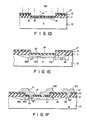
- the method for manufacturing a semiconductor device comprises: the step of forming a first silicon oxide film (11) on a major surface of a silicon substrate (10) of a first conductivity type; the step of selectively etching the first silicon oxide film (11) to form an opening (14); the step of forming a second silicon oxide film (16) on the silicon substrate (10) exposed through the opening (14); the step, performed at least one of before and after the step of forming the second silicon oxide film, of doping a first impurity in a portion of the silicon substrate (10) opposing the opening (14) using the first silicon oxide film (11) as a mask; the step of doping, into the second silicon oxide film (16), a second impurity of a second conductivity type, a diffusion rate of which in the silicon substrate (10) is higher than that of the first impurity in the silicon substrate (10), and a diffusion rate of which in the first silicon oxide film (11) is higher than that in the silicon substrate (10); and the step of diffusing the first impurity and the second im
- the second layer can be formed to be self-aligned with the first layer.
- the curvature of the second layer can be desirably set (1 to 50 degrees) in accordance with the thickness of the second silicon oxide film. For this reason, if the first layer is of p conductivity type and the second layer is of low-concentration p conductivity type, a high-breakdown voltage npn transistor can be manufactured like in the JTE method.
- the manufacturing method of the present invention requires only two ion-implantation processes and a single ion-diffusion process. Thus, the manufacturing processes are simpler and the yield is higher as compared to the guard ring and JTE methods.
- Fig. 3 shows the relationship between the film thickness of silicon oxide film 16 used for Ga diffusion and a degree of Ga diffusion in the lateral direction.
- a diffusion ratio (LD/xj) is increased as the film thickness of silicon oxide film 16 used for diffusion is increased. Therefore, the shape of low-concentration impurity layer 18a can be controllled by changing the film thickness of second silicon oxide film 16.
- Fig. 4 shows the results of breakdown voltage measurement of a p-n junction diode, constituted by low-concentration impurity layer 18a serving as a p-type base region and n-type silicon substrate 10 serving as a collector region, upon application of a voltage across base and collector electrodes 22 and 23 of the npn transistor (Figs. 1F and 2) manufactured by the above-mentioned processes. More specifically, Fig. 4 shows comparison results of p-n junction breakdown voltages in the present invention and the guard ring method when the diffusion ratio is set to be 1, 4, 8, and 16 (in this embodiment, since lateral diffusion distance LD is 200 ⁇ m and diffusion depth xj is 25 ⁇ m, diffusion ratio LD/xj is 8).
- a breakdown voltage about 90% of an ideal breakdown voltage (if the resistivity of an n-type silicon substrate is 60 ⁇ cm, 2100 V) could be obtained, and the structure of this embodiment was superior to that obtained by the conventional guard ring method having a breakdown voltage about 80% of the ideal breakdown voltage.
- substantially the same breakdown voltage as that of the JTE method could be obtained. If the diffusion ratio is increased, the breakdown voltage can be improved. Therefore, if the diffusion ratio is increased within a range of a pellet area of a device, the breakdown voltage can be further improved.
- low-concentration impurity layer 18a can be formed by simple processes to be self-aligned with and to surround high-concentration impurity layer 15a.
- the curvature of the junction portion of low-concentration impurity layer 18a can be large.
- a semiconductor device with a high breakdown voltage can be formed by simple processes to have a high yield.
- B ions are implanted in substrate 10.
- the present invention is not limited to this.
- boron ions may be implanted in substrate 10 through film 16.
- the ion-implantation conditions are a dose of 4 ⁇ 1014 cm ⁇ 2 and an acceleration energy of 10 keV.
- second silicon oxide film 16 is formed.
- a structure substantially the same as the structure having the first and second oxide films may be directly obtained from the structure shown in Fig. 1A by partially decreasing the thickness of silicon oxide film 11 by appropriately selecting the etching conditions.
- boron as a p-type impurity is used for forming high-concentration impurity layer 15a. If an n-type impurity, e.g., arsenic, is used in place of boron, n-type impurity layer 15a can be obtained.
- Fig. 5 shows the sectional structure of a transistor using arsenic instead of boron. In this case, since the diffusion rate of arsenic in silicon substrate 10 is lower than that of gallium in silicon substrate 10, the structure shown in Fig. 5 can be obtained.
- an npn transistor having n-type impurity layer 15a doped with arsenic as an emitter, p-type impurity layer 18a doped with gallium as a base, and n-type silicon substrate 10 as a collector can be obtained.
- An impurity implanted in second silicon oxide film 16 to form low-concentration impurity layer 18a is not limited to gallium. Atoms of any other element of a second conductivity type may be used if they have a higher diffusion rate in a silicon substrate than that of a first impurity in the silicon substrate and have a higher diffusion rate in the silicon oxide film than that in the silicon substrate. For example, aluminum (Al) may be used in place of gallium.
- a silicon nitride film is used as an insulating film in which the diffusion rate of gallium becomes lower than that in the silicon oxide film.
- a silicon carbide (SiC) film may be used.
- gallium (or aluminum) is doped using a mask. It is important for the present invention to dope gallium (or aluminum) in a silicon oxide film corresponding to a region in which boron ions are implanted. Therefore, upon formation of a relatively large element such as a power transistor, a spot size of an ion beam is decreased upon ion-implantation, so that the doping of gallium may be performed.
- the present invention is not limited to this.
- the present invention can be applied to semiconductor devices requiring a high-breakdown voltage, such as a diode, a high-breakdown voltage pnp transistor, a high-breakdown voltage MOS, and the like.
Landscapes
- Bipolar Transistors (AREA)
- Bipolar Integrated Circuits (AREA)
Applications Claiming Priority (2)
| Application Number | Priority Date | Filing Date | Title |
|---|---|---|---|
| JP238388/86 | 1986-10-07 | ||
| JP61238388A JPS6393153A (ja) | 1986-10-07 | 1986-10-07 | 半導体装置の製造方法 |
Publications (3)
| Publication Number | Publication Date |
|---|---|
| EP0263504A2 true EP0263504A2 (fr) | 1988-04-13 |
| EP0263504A3 EP0263504A3 (en) | 1989-10-18 |
| EP0263504B1 EP0263504B1 (fr) | 1993-01-07 |
Family
ID=17029453
Family Applications (1)
| Application Number | Title | Priority Date | Filing Date |
|---|---|---|---|
| EP87114619A Expired - Lifetime EP0263504B1 (fr) | 1986-10-07 | 1987-10-07 | Procédé pour la fabrication d'un dispositif semi-conducteur à haute tension de claquage |
Country Status (4)
| Country | Link |
|---|---|
| US (1) | US4780426A (fr) |
| EP (1) | EP0263504B1 (fr) |
| JP (1) | JPS6393153A (fr) |
| DE (1) | DE3783418T2 (fr) |
Cited By (3)
| Publication number | Priority date | Publication date | Assignee | Title |
|---|---|---|---|---|
| EP0527372A1 (fr) * | 1991-07-24 | 1993-02-17 | Canon Kabushiki Kaisha | Procédé pour la fabrication d'un transistor bipolaire |
| EP0762511A1 (fr) * | 1995-08-31 | 1997-03-12 | Nec Corporation | Transistor bipolaire et méthode de fabrication |
| CN113990767A (zh) * | 2021-10-28 | 2022-01-28 | 西安微电子技术研究所 | 一种电压法测试扩散结深的方法 |
Families Citing this family (8)
| Publication number | Priority date | Publication date | Assignee | Title |
|---|---|---|---|---|
| US6117719A (en) * | 1997-12-18 | 2000-09-12 | Advanced Micro Devices, Inc. | Oxide spacers as solid sources for gallium dopant introduction |
| US6806197B2 (en) * | 2001-08-07 | 2004-10-19 | Micron Technology, Inc. | Method of forming integrated circuitry, and method of forming a contact opening |
| US8106487B2 (en) | 2008-12-23 | 2012-01-31 | Pratt & Whitney Rocketdyne, Inc. | Semiconductor device having an inorganic coating layer applied over a junction termination extension |
| JP5452062B2 (ja) * | 2009-04-08 | 2014-03-26 | 三菱電機株式会社 | 炭化珪素半導体装置の製造方法 |
| JP5223773B2 (ja) | 2009-05-14 | 2013-06-26 | 三菱電機株式会社 | 炭化珪素半導体装置の製造方法 |
| JP6236456B2 (ja) * | 2013-09-09 | 2017-11-22 | 株式会社日立製作所 | 半導体装置およびその製造方法 |
| CN113178385B (zh) * | 2021-03-31 | 2022-12-23 | 青岛惠科微电子有限公司 | 一种芯片的制造方法、制造设备和芯片 |
| CN115472697A (zh) * | 2022-08-30 | 2022-12-13 | 西安电子科技大学杭州研究院 | 一种具有优化掺杂分布的氧化镓mosfet器件 |
Family Cites Families (12)
| Publication number | Priority date | Publication date | Assignee | Title |
|---|---|---|---|---|
| US3834953A (en) * | 1970-02-07 | 1974-09-10 | Tokyo Shibaura Electric Co | Semiconductor devices containing as impurities as and p or b and the method of manufacturing the same |
| FR2154294B1 (fr) * | 1971-09-27 | 1974-01-04 | Silec Semi Conducteurs | |
| JPS5538823B2 (fr) * | 1971-12-22 | 1980-10-07 | ||
| US4060427A (en) * | 1976-04-05 | 1977-11-29 | Ibm Corporation | Method of forming an integrated circuit region through the combination of ion implantation and diffusion steps |
| GB1548520A (en) * | 1976-08-27 | 1979-07-18 | Tokyo Shibaura Electric Co | Method of manufacturing a semiconductor device |
| JPS5388579A (en) * | 1977-01-13 | 1978-08-04 | Nec Corp | Production of semiconductor device |
| JPS5795625A (en) * | 1980-12-04 | 1982-06-14 | Toshiba Corp | Manufacture of semiconductor device |
| JPS57124427A (en) * | 1981-01-26 | 1982-08-03 | Toshiba Corp | Manufacture of semiconductor device |
| JPS5831519A (ja) * | 1981-08-18 | 1983-02-24 | Toshiba Corp | 半導体装置の製造方法 |
| DE3219888A1 (de) * | 1982-05-27 | 1983-12-01 | Deutsche Itt Industries Gmbh, 7800 Freiburg | Planares halbleiterbauelement und verfahren zur herstellung |
| JPS59210666A (ja) * | 1983-05-16 | 1984-11-29 | Nec Corp | 半導体装置 |
| JPS60117765A (ja) * | 1983-11-30 | 1985-06-25 | Fujitsu Ltd | 半導体装置の製造方法 |
-
1986
- 1986-10-07 JP JP61238388A patent/JPS6393153A/ja active Granted
-
1987
- 1987-09-24 US US07/101,026 patent/US4780426A/en not_active Expired - Lifetime
- 1987-10-07 EP EP87114619A patent/EP0263504B1/fr not_active Expired - Lifetime
- 1987-10-07 DE DE8787114619T patent/DE3783418T2/de not_active Expired - Fee Related
Cited By (5)
| Publication number | Priority date | Publication date | Assignee | Title |
|---|---|---|---|---|
| EP0527372A1 (fr) * | 1991-07-24 | 1993-02-17 | Canon Kabushiki Kaisha | Procédé pour la fabrication d'un transistor bipolaire |
| US5731240A (en) * | 1991-07-24 | 1998-03-24 | Canon Kabushiki Kaisha | Manufacturing method for semiconductor depositing device |
| EP0762511A1 (fr) * | 1995-08-31 | 1997-03-12 | Nec Corporation | Transistor bipolaire et méthode de fabrication |
| US5880516A (en) * | 1995-08-31 | 1999-03-09 | Nec Corporation | Semiconductor device utilizing a pedestal collector region and method of manufacturing the same |
| CN113990767A (zh) * | 2021-10-28 | 2022-01-28 | 西安微电子技术研究所 | 一种电压法测试扩散结深的方法 |
Also Published As
| Publication number | Publication date |
|---|---|
| DE3783418T2 (de) | 1993-05-27 |
| EP0263504B1 (fr) | 1993-01-07 |
| JPH0467781B2 (fr) | 1992-10-29 |
| JPS6393153A (ja) | 1988-04-23 |
| US4780426A (en) | 1988-10-25 |
| EP0263504A3 (en) | 1989-10-18 |
| DE3783418D1 (de) | 1993-02-18 |
Similar Documents
| Publication | Publication Date | Title |
|---|---|---|
| US4521952A (en) | Method of making integrated circuits using metal silicide contacts | |
| US4682405A (en) | Methods for forming lateral and vertical DMOS transistors | |
| KR100200059B1 (ko) | 쇼트키 장벽 다이오드 및 쇼트키 장벽 다이오드 클램프형 트랜지스터와 이들을 제조하는 방법 | |
| US4161417A (en) | Method of making CMOS structure with retarded electric field for minimum latch-up | |
| US4583106A (en) | Fabrication methods for high performance lateral bipolar transistors | |
| EP0137905B1 (fr) | Procédé pour la fabrication de transistors bipolaires latéraux | |
| EP0137906A1 (fr) | Procédé de fabrication de transistors NPN verticaux et PNP latéraux dans le même corps semiconducteur | |
| US4412378A (en) | Method for manufacturing semiconductor device utilizing selective masking, etching and oxidation | |
| EP0345435B2 (fr) | Dispositif semi-conducteur à haute tension de claquage et procédé pour sa fabrication | |
| US4375717A (en) | Process for producing a field-effect transistor | |
| EP0232510B1 (fr) | Dispositif semi-conducteur à jonction plane à bords autopassivants | |
| US4619036A (en) | Self-aligned low-temperature emitter drive-in | |
| EP0263504B1 (fr) | Procédé pour la fabrication d'un dispositif semi-conducteur à haute tension de claquage | |
| JP2673943B2 (ja) | P型領域に低抵抗オーム接点を形成する方法 | |
| EP0579502A2 (fr) | Suppresseur de surtension transitoire à l'état solide | |
| US4724221A (en) | High-speed, low-power-dissipation integrated circuits | |
| JPH0241170B2 (fr) | ||
| EP0221742B1 (fr) | Procédé de fabrication de circuit intégré pour former un transistor bipolaire ayant des régions de base extrinsèques | |
| EP0974165B1 (fr) | Dispositif semi-conducteur a transistor bipolaire, et procede de fabrication associe | |
| EP0036499B1 (fr) | Procédé auto-aligné pour transistor bipolaire à base en polysilicium | |
| US5298437A (en) | Fabrication process for Schottky barrier diodes on a single poly bipolar process | |
| KR0161378B1 (ko) | 바이폴라 접합 트랜지스터 제조방법 | |
| US3925105A (en) | Process for fabricating integrated circuits utilizing ion implantation | |
| US5925923A (en) | Merged single polysilicon bipolar NPN transistor | |
| US5376563A (en) | Method of manufacturing an emitter base self alignment structure |
Legal Events
| Date | Code | Title | Description |
|---|---|---|---|
| PUAI | Public reference made under article 153(3) epc to a published international application that has entered the european phase |
Free format text: ORIGINAL CODE: 0009012 |
|
| 17P | Request for examination filed |
Effective date: 19871007 |
|
| AK | Designated contracting states |
Kind code of ref document: A2 Designated state(s): DE FR GB |
|
| PUAL | Search report despatched |
Free format text: ORIGINAL CODE: 0009013 |
|
| AK | Designated contracting states |
Kind code of ref document: A3 Designated state(s): DE FR GB |
|
| 17Q | First examination report despatched |
Effective date: 19910828 |
|
| GRAA | (expected) grant |
Free format text: ORIGINAL CODE: 0009210 |
|
| AK | Designated contracting states |
Kind code of ref document: B1 Designated state(s): DE FR GB |
|
| REF | Corresponds to: |
Ref document number: 3783418 Country of ref document: DE Date of ref document: 19930218 |
|
| ET | Fr: translation filed | ||
| PLBE | No opposition filed within time limit |
Free format text: ORIGINAL CODE: 0009261 |
|
| STAA | Information on the status of an ep patent application or granted ep patent |
Free format text: STATUS: NO OPPOSITION FILED WITHIN TIME LIMIT |
|
| 26N | No opposition filed | ||
| REG | Reference to a national code |
Ref country code: GB Ref legal event code: 746 Effective date: 19980909 |
|
| REG | Reference to a national code |
Ref country code: FR Ref legal event code: D6 |
|
| REG | Reference to a national code |
Ref country code: GB Ref legal event code: IF02 |
|
| PGFP | Annual fee paid to national office [announced via postgrant information from national office to epo] |
Ref country code: GB Payment date: 20021002 Year of fee payment: 16 |
|
| PGFP | Annual fee paid to national office [announced via postgrant information from national office to epo] |
Ref country code: FR Payment date: 20021008 Year of fee payment: 16 |
|
| PGFP | Annual fee paid to national office [announced via postgrant information from national office to epo] |
Ref country code: DE Payment date: 20021011 Year of fee payment: 16 |
|
| PG25 | Lapsed in a contracting state [announced via postgrant information from national office to epo] |
Ref country code: GB Free format text: LAPSE BECAUSE OF NON-PAYMENT OF DUE FEES Effective date: 20031007 |
|
| PG25 | Lapsed in a contracting state [announced via postgrant information from national office to epo] |
Ref country code: DE Free format text: LAPSE BECAUSE OF NON-PAYMENT OF DUE FEES Effective date: 20040501 |
|
| GBPC | Gb: european patent ceased through non-payment of renewal fee |
Effective date: 20031007 |
|
| PG25 | Lapsed in a contracting state [announced via postgrant information from national office to epo] |
Ref country code: FR Free format text: LAPSE BECAUSE OF NON-PAYMENT OF DUE FEES Effective date: 20040630 |
|
| REG | Reference to a national code |
Ref country code: FR Ref legal event code: ST |