EP0263631A2 - Composant électrique connecté et méthode - Google Patents
Composant électrique connecté et méthode Download PDFInfo
- Publication number
- EP0263631A2 EP0263631A2 EP87308603A EP87308603A EP0263631A2 EP 0263631 A2 EP0263631 A2 EP 0263631A2 EP 87308603 A EP87308603 A EP 87308603A EP 87308603 A EP87308603 A EP 87308603A EP 0263631 A2 EP0263631 A2 EP 0263631A2
- Authority
- EP
- European Patent Office
- Prior art keywords
- conductors
- pcb
- holes
- rigid
- conductive
- Prior art date
- Legal status (The legal status is an assumption and is not a legal conclusion. Google has not performed a legal analysis and makes no representation as to the accuracy of the status listed.)
- Withdrawn
Links
Images



Classifications
-
- H—ELECTRICITY
- H01—ELECTRIC ELEMENTS
- H01R—ELECTRICALLY-CONDUCTIVE CONNECTIONS; STRUCTURAL ASSOCIATIONS OF A PLURALITY OF MUTUALLY-INSULATED ELECTRICAL CONNECTING ELEMENTS; COUPLING DEVICES; CURRENT COLLECTORS
- H01R12/00—Structural associations of a plurality of mutually-insulated electrical connecting elements, specially adapted for printed circuits, e.g. printed circuit boards [PCB], flat or ribbon cables, or like generally planar structures, e.g. terminal strips, terminal blocks; Coupling devices specially adapted for printed circuits, flat or ribbon cables, or like generally planar structures; Terminals specially adapted for contact with, or insertion into, printed circuits, flat or ribbon cables, or like generally planar structures
- H01R12/50—Fixed connections
- H01R12/51—Fixed connections for rigid printed circuits or like structures
- H01R12/52—Fixed connections for rigid printed circuits or like structures connecting to other rigid printed circuits or like structures
- H01R12/523—Fixed connections for rigid printed circuits or like structures connecting to other rigid printed circuits or like structures by an interconnection through aligned holes in the boards or multilayer board
-
- H—ELECTRICITY
- H05—ELECTRIC TECHNIQUES NOT OTHERWISE PROVIDED FOR
- H05K—PRINTED CIRCUITS; CASINGS OR CONSTRUCTIONAL DETAILS OF ELECTRIC APPARATUS; MANUFACTURE OF ASSEMBLAGES OF ELECTRICAL COMPONENTS
- H05K1/00—Printed circuits
- H05K1/02—Details
- H05K1/14—Structural association of two or more printed circuits
- H05K1/144—Stacked arrangements of planar printed circuit boards
-
- H—ELECTRICITY
- H05—ELECTRIC TECHNIQUES NOT OTHERWISE PROVIDED FOR
- H05K—PRINTED CIRCUITS; CASINGS OR CONSTRUCTIONAL DETAILS OF ELECTRIC APPARATUS; MANUFACTURE OF ASSEMBLAGES OF ELECTRICAL COMPONENTS
- H05K7/00—Constructional details common to different types of electric apparatus
- H05K7/02—Arrangements of circuit components or wiring on supporting structure
-
- H—ELECTRICITY
- H05—ELECTRIC TECHNIQUES NOT OTHERWISE PROVIDED FOR
- H05K—PRINTED CIRCUITS; CASINGS OR CONSTRUCTIONAL DETAILS OF ELECTRIC APPARATUS; MANUFACTURE OF ASSEMBLAGES OF ELECTRICAL COMPONENTS
- H05K7/00—Constructional details common to different types of electric apparatus
- H05K7/02—Arrangements of circuit components or wiring on supporting structure
- H05K7/026—Multiple connections subassemblies
-
- H—ELECTRICITY
- H01—ELECTRIC ELEMENTS
- H01H—ELECTRIC SWITCHES; RELAYS; SELECTORS; EMERGENCY PROTECTIVE DEVICES
- H01H11/00—Apparatus or processes specially adapted for the manufacture of electric switches
- H01H11/0006—Apparatus or processes specially adapted for the manufacture of electric switches for converting electric switches
- H01H11/0031—Apparatus or processes specially adapted for the manufacture of electric switches for converting electric switches for allowing different types or orientation of connections to contacts
-
- H—ELECTRICITY
- H01—ELECTRIC ELEMENTS
- H01H—ELECTRIC SWITCHES; RELAYS; SELECTORS; EMERGENCY PROTECTIVE DEVICES
- H01H43/00—Time or time-programme switches providing a choice of time-intervals for executing one or more switching actions and automatically terminating their operation after the programme is completed
- H01H43/02—Details
- H01H43/024—Terminal arrangements
-
- H—ELECTRICITY
- H05—ELECTRIC TECHNIQUES NOT OTHERWISE PROVIDED FOR
- H05K—PRINTED CIRCUITS; CASINGS OR CONSTRUCTIONAL DETAILS OF ELECTRIC APPARATUS; MANUFACTURE OF ASSEMBLAGES OF ELECTRICAL COMPONENTS
- H05K2201/00—Indexing scheme relating to printed circuits covered by H05K1/00
- H05K2201/10—Details of components or other objects attached to or integrated in a printed circuit board
- H05K2201/10227—Other objects, e.g. metallic pieces
- H05K2201/10295—Metallic connector elements partly mounted in a hole of the PCB
- H05K2201/10303—Pin-in-hole mounted pins
-
- H—ELECTRICITY
- H05—ELECTRIC TECHNIQUES NOT OTHERWISE PROVIDED FOR
- H05K—PRINTED CIRCUITS; CASINGS OR CONSTRUCTIONAL DETAILS OF ELECTRIC APPARATUS; MANUFACTURE OF ASSEMBLAGES OF ELECTRICAL COMPONENTS
- H05K2201/00—Indexing scheme relating to printed circuits covered by H05K1/00
- H05K2201/10—Details of components or other objects attached to or integrated in a printed circuit board
- H05K2201/10613—Details of electrical connections of non-printed components, e.g. special leads
- H05K2201/10742—Details of leads
- H05K2201/1075—Shape details
- H05K2201/10871—Leads having an integral insert stop
-
- H—ELECTRICITY
- H05—ELECTRIC TECHNIQUES NOT OTHERWISE PROVIDED FOR
- H05K—PRINTED CIRCUITS; CASINGS OR CONSTRUCTIONAL DETAILS OF ELECTRIC APPARATUS; MANUFACTURE OF ASSEMBLAGES OF ELECTRICAL COMPONENTS
- H05K2201/00—Indexing scheme relating to printed circuits covered by H05K1/00
- H05K2201/10—Details of components or other objects attached to or integrated in a printed circuit board
- H05K2201/10613—Details of electrical connections of non-printed components, e.g. special leads
- H05K2201/10742—Details of leads
- H05K2201/10886—Other details
- H05K2201/10939—Lead of component used as a connector
-
- H—ELECTRICITY
- H05—ELECTRIC TECHNIQUES NOT OTHERWISE PROVIDED FOR
- H05K—PRINTED CIRCUITS; CASINGS OR CONSTRUCTIONAL DETAILS OF ELECTRIC APPARATUS; MANUFACTURE OF ASSEMBLAGES OF ELECTRICAL COMPONENTS
- H05K3/00—Apparatus or processes for manufacturing printed circuits
- H05K3/30—Assembling printed circuits with electric components, e.g. with resistors
- H05K3/32—Assembling printed circuits with electric components, e.g. with resistors electrically connecting electric components or wires to printed circuits
- H05K3/34—Assembling printed circuits with electric components, e.g. with resistors electrically connecting electric components or wires to printed circuits by soldering
- H05K3/3447—Lead-in-hole components
Definitions
- the present invention relates to an electrically terminated component of the type having a group of stiff conductors exiting a casing or housing, eg over a surface or side thereof so that at least a group thereof point generally in the same direction but are grouped in an arbitrary but definite pattern.
- the invention also relates to a method of terminating a component.
- Such components are often sold to several different customers, such as washing machine programmer-timer units which may be sold to many different domestic appliance manufacturers for incorporation in their products.
- the component supplier In order to have all the components uniform, with rigid conductors issuing at the same points on the housing, the component supplier sometimes wires up an external adapter or socket and plug arrangement to regroup the conductors, but this solution is expensive in time, and bulk is added to the component. Flexible or flying leads on components are not usually desirable.
- the present invention enables components to be manufactured uniformly with rigid exiting conductors but terminated in individual groupings, by use of attachment of a pair of stacked printed circuit boards (PCB's) each having conductive through holes participating in printed patterns, of rigid conductors bonded through said holes of both PCB's, and of extensions of said rigid exiting conductors bonded through said holes of at least the inner PCB, the inner PCB preferably resting flat against projecting portions of the component housing, and the holes of the outer PCB accommodating anchoring pins of external terminals.
- PCB's printed circuit boards
- a component 1 such as an electro-mechanical programmer has exit conductor positions shown as dark dots 2 eg in four groups separated by thin insulating, conveniently parallel, partition walls 3.
- the walls are seen edge-on in Figure 1 and form insulating projections from the casing of the component walls and the conductors extend directly towards the viewer in Figure 1, ie all in the same direction.
- the conductors may be for programmed supplies to motors, heaters, water valves, pumps or other units in domestic apparatus.
- Two customers may like the component 1 but one may not select it from the manufacturer because of undesirable groupings of the conductor positions 2. It is highly inconvenient to manufacture different versions of the component having conductors at different positions 2.
- the invention enables one version to be terminated in very many different ways, so that most if not all customers can be suited without undue expense.
- FIG. 2 Referring to the side view of Figure 2, four conductors 4 can be seen and will occupy four of the positions 2 of Figure 1. Others will occupy different planes and be non-represented or invisible in Figure 2.
- a first, inner PCB 5 rests against the edges of the walls 3 which define a surface, and elongations 6, 7 of the conductors 4 pass through holes of a first set of conductive through-holes in PCB 5.
- Relatively shorter elongations 6 extend only a short distance out beyond inner PCB 5, while other conductors 4 have relatively longer elongations 7 which extend further out, and pass also through aligned holes of a second set of through-holes in a second, outer PCB 8 stacked parallel to the inner PCB.
- Some, or all of the two sets of through-holes may form aligned pairs which can accommodate such elongations 7.
- the elongations are bonded eg by soldering to the through-holes passed through, so that the PCB's are located relative to the component 1.
- the inner PCB 5 is as aforesaid further supported by resting on the edges of walls 3.
- short conductive pins or pegs 9 extend just through both PCB's at aligned holes therein, being likewise soldered thereto.
- the short pins 9 perform at least a structural function, in holding and bracing the outer PCB to the inner one. At least some, indeed possibly all of the soldered pins and elongations 6, 7 and 9 may also function electrically with the printed conductors on the boards as will become apparent.
- the actual depths as viewed of conductors 4 and the elongations and pins cannot be ascertained since they are grouped in various planes.
- fastons 10 or other male connectors are also grouped in various planes, according to desirability or requirement of a customer.
- Printed tracks on boards 5, 8 will determine not only which faston connectors 10 are connected to which component conductors 4 according to the principal object of the invention; but also, by an option, interconnections between the fastons can be selectively made.
- a customer's requirement can be served, which prior to this invention would have had to be met by the customer.
- a conductor 4 conveniently is flat, has a waist 11 where it passes through the housing, is tapered at 12 to a support shoulder 13 and then terminates in a short elongation 6, or, see Figure 4, in a long pin-like elongation 7.
- pins 9 are used, they can resemble the elongations 7, being pointed at one or both ends for ease in assembling in the through-holes.
- the preferred materials for the conductors, pins, elongations etc are copper and its alloys.
- the support shoulder 13 provides structural support additional to that provided by the soldered joint at the through hole, and additional or alternative to that of the projections 3.
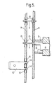
- Figure 5 shows more visibly details of Figure 2, namely housing projecting walls 3, a rigid exiting conductor 4, PCB supporting shoulder 13, PCB's 5 and 8, a relatively longer elongation 7 and a pin 9 (soldered) in aligned through-holes, and a faston 10 having two mounting pins 14 soldered in further conductive through-holes in the outer PCB 8.
- a support shoulder (none shown) can also be provided near the outer ends of the longer elongations 7, or of the pins 9, for the outer PCB to rest on.
- the through holes in the two PCB's will then need to be of different sizes or diameters, because the shoulders of elongations 7 will have to be passed through the holes of the inner PCB before abutting the outer PCB.
- Figure 5 also shows that, as conventional, the plating of the through-holes extends at the flat portions at 15 on one or both sides of the two PCB's, for their inclusion in the printed circuitry on the one or both sides required.
- one or both PCB's may have no printed circuitry on the eg inner side, accordingly this embodiment has inner PCB 5 with the pattern shown on Figure 6 on its outer side only. All the through holes 16, which it will be recalled are in four groups separated by the lines of abutment of the inner side with walls 3, are involved in the pattern. Some of the through-hole positions will correspond exactly with those of the rigid exit conductors 4, and others 17 are used for pins 9 which are not necessarily in circuit, but the pattern could vary from customer to customer because it cooperates with the outer PCB circuitry, which of course usually will also vary from customer to customer.
- the outer PCB circuitry in one example is as shown in Figure 7 on the inner side and in Figure 8 on the outer side.
- the through-holes may be unused structurally or electrically, or accommodate pins 9, long elongations 7 or (in pairs) fastons 10.
- the inner or outer or both patterns may include them.
- Designing the circuitry involves often a computer optimization, ie for minimum complications, crossovers, undue lengths, undue thicknesses in combination with length, and tracks at different voltages or at different power phases etc being closer than 3mm etc.
- the customer manufacturer may have one group of say five female connectors in one socket body, participating in a harness (without cross-overs as has been discussed herein), but he would be quite happy to select plugging in with either of the two rotations of this body, relative to all the other sockets from the harness.
- This allows more freedom in the detailed circuit design of the inventive PCB's because the corresponding five males or fastons can be connected in circuit in one of two ways, either in one order or its reverse.
- Such considerations are routine to modern planar circuit designers and their computer aids.
- printing of heater feeds is a problem, eg up to 15-16 amps, for which accepted standards call for conductors 0,7 sq mm in cross-section.
- Some appliance manufacturers are happy to incorporate a relay, at least for the heater feed, so that the PCB need only cater for the relay drive current.
- the motor current for spin-drying is usually the next most severe consideration, ie location of these preferably shortest, and necessarily thickest tracks can take first priority at the design stage.
- PCB's designed (eg computer aided) having regard to local electrical and/or environmental standards, to customer requirements (eg non-crossover wiring runs), and possible freedom as to the one or or the reverse order of consecutive groups of said plug conductors.
Landscapes
- Engineering & Computer Science (AREA)
- Microelectronics & Electronic Packaging (AREA)
- Coupling Device And Connection With Printed Circuit (AREA)
Applications Claiming Priority (2)
| Application Number | Priority Date | Filing Date | Title |
|---|---|---|---|
| GB8624374 | 1986-10-10 | ||
| GB8624374A GB8624374D0 (en) | 1986-10-10 | 1986-10-10 | Terminated electrical component |
Publications (2)
| Publication Number | Publication Date |
|---|---|
| EP0263631A2 true EP0263631A2 (fr) | 1988-04-13 |
| EP0263631A3 EP0263631A3 (fr) | 1989-12-06 |
Family
ID=10605564
Family Applications (1)
| Application Number | Title | Priority Date | Filing Date |
|---|---|---|---|
| EP87308603A Withdrawn EP0263631A3 (fr) | 1986-10-10 | 1987-09-29 | Composant électrique connecté et méthode |
Country Status (2)
| Country | Link |
|---|---|
| EP (1) | EP0263631A3 (fr) |
| GB (1) | GB8624374D0 (fr) |
Cited By (3)
| Publication number | Priority date | Publication date | Assignee | Title |
|---|---|---|---|---|
| FR2686763A1 (fr) * | 1992-01-29 | 1993-07-30 | Mecanismos Aux Ind | Procede de fabrication de boites de jonction pour vehicules. |
| GB2287139A (en) * | 1994-03-02 | 1995-09-06 | Mecanismos Aux Ind | Electrical terminal mounting arrangement |
| EP1487247A1 (fr) * | 2003-06-13 | 2004-12-15 | Sumitomo Wiring Systems, Ltd. | Boítier de connecteur électrique |
Family Cites Families (5)
| Publication number | Priority date | Publication date | Assignee | Title |
|---|---|---|---|---|
| US4054939A (en) * | 1975-06-06 | 1977-10-18 | Elfab Corporation | Multi-layer backpanel including metal plate ground and voltage planes |
| US4208080A (en) * | 1976-08-18 | 1980-06-17 | Amp Incorporated | Junction boxes |
| US4084869A (en) * | 1976-11-10 | 1978-04-18 | Intel Corporation | Interconnector for integrated circuit package |
| US4331370A (en) * | 1980-04-28 | 1982-05-25 | Amp Incorporated | Connection system for printed circuit boards |
| JPS614172A (ja) * | 1984-06-18 | 1986-01-10 | ファナック株式会社 | 交流電動機制御盤 |
-
1986
- 1986-10-10 GB GB8624374A patent/GB8624374D0/en active Pending
-
1987
- 1987-09-29 EP EP87308603A patent/EP0263631A3/fr not_active Withdrawn
Cited By (7)
| Publication number | Priority date | Publication date | Assignee | Title |
|---|---|---|---|---|
| FR2686763A1 (fr) * | 1992-01-29 | 1993-07-30 | Mecanismos Aux Ind | Procede de fabrication de boites de jonction pour vehicules. |
| ES2071540A1 (es) * | 1992-01-29 | 1995-06-16 | Mecanismos Aux Ind | Perfeccionamientos en los procesos de fabricacion de cajas de servicios y de sus partes. |
| GB2287139A (en) * | 1994-03-02 | 1995-09-06 | Mecanismos Aux Ind | Electrical terminal mounting arrangement |
| FR2717005A1 (fr) * | 1994-03-02 | 1995-09-08 | Mecanismos Aux Ind | Temporisateur perfectionné. |
| GB2287139B (en) * | 1994-03-02 | 1997-10-22 | Mecanismos Aux Ind | Timer |
| EP1487247A1 (fr) * | 2003-06-13 | 2004-12-15 | Sumitomo Wiring Systems, Ltd. | Boítier de connecteur électrique |
| US6984133B2 (en) | 2003-06-13 | 2006-01-10 | Sumitomo Wiring Systems, Ltd. | Electrical connector housing having a bridging piece between circuit boards connected to a receiving unit |
Also Published As
| Publication number | Publication date |
|---|---|
| EP0263631A3 (fr) | 1989-12-06 |
| GB8624374D0 (en) | 1986-11-12 |
Similar Documents
| Publication | Publication Date | Title |
|---|---|---|
| EP0240453B1 (fr) | Boîte de jonction programmable | |
| US3723635A (en) | Double-sided flexible circuit assembly and method of manufacture therefor | |
| US4689023A (en) | Programmable electrical connector | |
| US4871317A (en) | Surface mounted component adaptor for interconnecting of surface mounted circuit components | |
| US5325267A (en) | Remote driver board having input/output connector circuitry molded therein | |
| EP0039175A2 (fr) | Assemblage de connecteurs électriques pour des plaquettes à circuits imprimés | |
| EP0086961A2 (fr) | Plaquette multicouche pour l'interconnexion de circuits grande vitesse | |
| US5040996A (en) | Central circuit arrangement for motor vehicles | |
| JPS6013413A (ja) | ワイヤリングハ−ネスの相互接続装置 | |
| EP0970594A1 (fr) | Supports moules pour la fixation de composants electroniques | |
| US6016253A (en) | Electronic module | |
| US2951184A (en) | Printed wiring assembly | |
| US5667401A (en) | Cable connector, circuit board and system having circuit boards connected together by the cable connector | |
| JP3815154B2 (ja) | 電気接続箱 | |
| CA1047637A (fr) | Panneau multi-couche avec boitier a sorties alignees pour circuit logique de commutation a grande vitesse | |
| EP0481778A1 (fr) | Moyens de connexion pour une structure de bus | |
| EP0643449B1 (fr) | Connecteur pour câble-ruban | |
| EP0263631A2 (fr) | Composant électrique connecté et méthode | |
| JP3876563B2 (ja) | 電気接続箱 | |
| US5616034A (en) | Power supply apparatus for package | |
| US4508398A (en) | Printed circuit connecting device | |
| US4895524A (en) | Interface device having rigid planar elements and flexible printed circuits | |
| US6467163B1 (en) | Universal component mounting structure for surface mountable electronic devices | |
| US4518211A (en) | Device for mounting, interconnecting and terminating printed circuits | |
| US4226492A (en) | Electrical interconnection apparatus |
Legal Events
| Date | Code | Title | Description |
|---|---|---|---|
| PUAI | Public reference made under article 153(3) epc to a published international application that has entered the european phase |
Free format text: ORIGINAL CODE: 0009012 |
|
| AK | Designated contracting states |
Kind code of ref document: A2 Designated state(s): DE FR GB IT |
|
| RAP3 | Party data changed (applicant data changed or rights of an application transferred) |
Owner name: EATON CONTROLS SPA |
|
| PUAL | Search report despatched |
Free format text: ORIGINAL CODE: 0009013 |
|
| AK | Designated contracting states |
Kind code of ref document: A3 Designated state(s): DE FR GB IT |
|
| STAA | Information on the status of an ep patent application or granted ep patent |
Free format text: STATUS: THE APPLICATION IS DEEMED TO BE WITHDRAWN |
|
| 18D | Application deemed to be withdrawn |
Effective date: 19900507 |
|
| RIN1 | Information on inventor provided before grant (corrected) |
Inventor name: RILEY, JOHN GRANT Inventor name: DOUTRIAUX, JEAN LUC |