EP0263907A1 - Einrichtung zur parallelen Verarbeitung von Steuersignalen in einem "Fanin/Fanout"-Modem - Google Patents
Einrichtung zur parallelen Verarbeitung von Steuersignalen in einem "Fanin/Fanout"-Modem Download PDFInfo
- Publication number
- EP0263907A1 EP0263907A1 EP86430039A EP86430039A EP0263907A1 EP 0263907 A1 EP0263907 A1 EP 0263907A1 EP 86430039 A EP86430039 A EP 86430039A EP 86430039 A EP86430039 A EP 86430039A EP 0263907 A1 EP0263907 A1 EP 0263907A1
- Authority
- EP
- European Patent Office
- Prior art keywords
- signal
- dte
- outgoing
- incoming
- register
- Prior art date
- Legal status (The legal status is an assumption and is not a legal conclusion. Google has not performed a legal analysis and makes no representation as to the accuracy of the status listed.)
- Withdrawn
Links
Images


Classifications
-
- G—PHYSICS
- G06—COMPUTING OR CALCULATING; COUNTING
- G06F—ELECTRIC DIGITAL DATA PROCESSING
- G06F13/00—Interconnection of, or transfer of information or other signals between, memories, input/output devices or central processing units
- G06F13/14—Handling requests for interconnection or transfer
- G06F13/36—Handling requests for interconnection or transfer for access to common bus or bus system
- G06F13/362—Handling requests for interconnection or transfer for access to common bus or bus system with centralised access control
- G06F13/364—Handling requests for interconnection or transfer for access to common bus or bus system with centralised access control using independent requests or grants, e.g. using separated request and grant lines
-
- H—ELECTRICITY
- H04—ELECTRIC COMMUNICATION TECHNIQUE
- H04L—TRANSMISSION OF DIGITAL INFORMATION, e.g. TELEGRAPHIC COMMUNICATION
- H04L5/00—Arrangements affording multiple use of the transmission path
Definitions
- the invention relates to fanin / fanout modems, and more particularly to a device for parallel processing of control signals in a fanin / fanout modem.
- each DTE is equipped with a modem where the carrier signal is modulated by the data in a modulator on the transmission side and demodulated in a receiver side receiver.
- the multiplexer allows the modem to be connected to several DTEs which receive or transmit data according to the principle of time multiplexing. That is to say that each byte of data which transits on the single transmission line, is formed by the juxtaposition of groups of bits originating from or bound for each DTE, the number of bits in each group depending on the speed. assigned to the corresponding DTE.
- the modem is also connected to several DTEs, but there is no data multiplexing.
- data from the local modem is received by the modem, it is transmitted simultaneously to all the DTEs which are connected to it.
- each DTE transmits its data in turn. To do this, it requests to transmit a data message by sending a transmission request signal (RTS) to the modem. If no DTE is being transmitted, the modem then sends a transmission acceptance signal (RFS) to the DTE which indicates to the DTE that it can proceed with the transmission of its message.
- RTS transmission request signal
- each DTE we therefore thought of allowing each DTE to send its RTS signal to the modem without a call procedure being launched.
- This signal is loaded into a DTE-specific interface register located in the modem. Since several DTEs can send their RTS signal at the same time, the modem signal processor repetitively performs a scan procedure of each DTE interface register, allowing the processor to allocate the transmission line to the DTE which requests it. insofar as another DTE is not transmitting.
- Such a procedure, involving a routine of the processor control software has the disadvantage of consuming a lot of processing time, since the scanning routine must be repeated for each interface register of DTE and this at each baud time.
- the object of the invention is therefore a device for parallel processing of the control signals, and in particular of the transmission request signals (RTS), in a modem of the fanin / fanout type, thus avoiding having to repeat the same processing procedure for each DTE connected to the modem.
- RTS transmission request signals
- the device comprises an interface register associated with each DTE, intended to load bits representing incoming control signals and outgoing control signals for the associated DTE; an incoming command signal register the content of which is a word formed by the bits originating from each of the interface registers and representing the incoming command signal; an outgoing control signal register the content of which is a word formed by the bits each representing the outgoing control signal for each DTE; the modem signal processor comprising control means which provide the word loaded in the outgoing command signal register in response to the word in the incoming command signal register, and authorization means for authorizing the transfer of bits forming the word loaded in the outgoing control signal register in the interface registers associated with the DTEs.
- DTE data terminal equipment
- fanin / fanout parallel distribution modem
- the modem is connected to 4 DTEs which are identified by the letters A, B, C and D.
- the modem therefore has 4 interface registers: 2-A, 2-B, 2 -C and 2-D respectively associated with DTE A, B, C and D not shown in the figure.
- Each interface register records bits corresponding to so-called incoming control signals when they come from the DTE, and bits corresponding to so-called outgoing control signals when they are intended for the DTE.
- a DTE For example A, wishes to transmit data it activates the transmission request control signal (RTS) and a bit "1" is loaded in the RTS position of the interface register 2-A of the modem.
- RTS transmission request control signal
- a bit "1" is loaded in the RTS position of the interface register 2-A of the modem.
- RTS transmission request control signal
- the set of RTS bits of the DTE interface registers which forms a 4-bit word is loaded into the RTS register 4.
- This word is transmitted by the bus 12 to the decoding and priority block 6.
- the block 6 also receives as input the bus 16 which provides a 4-bit word formed by the output bits at the previous baud time, from the decoding block and priority 6 on the bus 14, after delay of a baud time by the circuit to delay 8.
- the function of the decoding and priority block is to process in parallel, at each baud time, the word found in the RTS register, to supply a word formed of 4 bits also representing each the transmission acceptance signal ( RFS) for the corresponding DTE, this taking into account a certain number of parameters such as the respect of an order of priority among the DTE or else the non-interruption of a transmission in progress.
- RFS transmission acceptance signal
- Such a block can be implemented in software located in the memory of the signal processor of the modem, or in the form of a circuit as will be seen in connection with FIG. 2.
- an authorization signal supplied by the modem processor conditions (or not) the AND gate 18 to allow the content of register 10 to be loaded into the RFS positions of the DTE interface registers 2-A to 2-D .
- the authorization which enables the AND gate 18 to pass is intended to allow the modem time to initialize the transmission. Indeed, when one of the DTE requests to transmit and activates its RTS signal, while no DTE occupies the line, the modem initiates the procedure for transmitting the initialization sequence which precedes any data transfer. This initialization sequence must have a minimum duration allowing the receiving modem to be ready (for example to adapt its equalizer) to receive the following data. It is only when this minimum duration has elapsed that the processor delivers the authorization signal to the gate AND 18 at each baud time, and this is so as long as this transmission lasts.
- gate 26-A being active, it is inverted by the inverter 28 which provides a "zero" at the input of AND gate 38. Consequently, gate 38 is blocked and does not allow the RTS-B signal to be transmitted further.
- the active output of the gate 26-A also provides, by the OR circuit 34 and the inverter 30 on the one hand, and by the OR circuit 36 and the inverter 32 on the other hand, the blocking of the doors ET 40 and ET 42, which would also inhibit the outputs of gates 26-C and 26-D if they were "one" following the activation of lines RTS-C and RTS-D. It can therefore be seen that only the line RFS-A of the bus 14 is active when A requests to transmit, whatever the requests of the other DTE B, C or D.
- the inverter 22 provides a "zero" at the output which inhibits the gates 26 B, C, and D, as we saw previously, so that the activation of one or more of the other RTS lines is not not taken into account. This also applies to the case where another DTE than A is in the transmission procedure (its RTS is active). In summary, the activation of an RTS line, for more than one baud time, inhibits the possible activation of the other RTS lines, regardless of the priority assigned to DTEs.
- An additional condition may be taken into account at the same time as the incoming control signal such as RTS.
- the condition is stored in a position in the DTE interface register in the same way as the control signals.
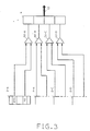
- FIG. 3 shows the hardware implementation taking into account the condition that the DTE is well supplied (PO).
- a position of each of the interface registers 2-A to 2-D contains a bit PO which takes the value "1" if the DTE is supplied correctly and "0" otherwise.
- the bit PO of DTE A is at "zero” indicating that this terminal is not capable of transmitting although its RTS bit is active, this last bit cannot be transferred to register 4 since the AND circuit 50-A is blocked.
- the AND circuits 50-B, 50-C, 50-D are respectively blocked by the "zero" bits of the associated DTE B, C and D, thus preventing the transfer of the corresponding RTS signals.
- the invention has been illustrated by considering the case of RTS transmission request signals as incoming control signals and transmission acceptance signals as outgoing control signals. But it goes without saying that the invention is not limited to this single case.
- the incoming control signals could be test request request signals.
- the parallel processing performed by the signal processor would be different from that of the RTS signals.
- This processing carried out using logic circuits would require an arrangement different from that illustrated in FIGS. 2 and 3 since meeting other parameters and conditions than the processing of the transmission request signals.
- the output word would then be formed of test acceptance signals. Unlike RFS transmission acceptance signals where only one of the 4 bits is "one" since only one DTE can transmit data at any given time on the single transmission line, there could be several acceptance bits of test equal to "one" in the output word, several of the DTEs being able to carry out their test simultaneously.
- the invention has been described in detail for the particular case of transmission control signals, it is clear that it can be used for other cases of control signals in a modem of the fanin / fanout type.
- one of the essential characteristics being the parallel processing of a word formed by the bits representing an incoming control signal for each DTE, so as to provide a word formed by the bits representing an outgoing control signal for each DTE, it being understood that this parallel processing can be implemented either by hardware or by software for controlling the signal processor.
Landscapes
- Engineering & Computer Science (AREA)
- Signal Processing (AREA)
- Theoretical Computer Science (AREA)
- Computer Networks & Wireless Communication (AREA)
- Physics & Mathematics (AREA)
- General Engineering & Computer Science (AREA)
- General Physics & Mathematics (AREA)
- Communication Control (AREA)
- Time-Division Multiplex Systems (AREA)
Priority Applications (2)
| Application Number | Priority Date | Filing Date | Title |
|---|---|---|---|
| EP86430039A EP0263907A1 (de) | 1986-10-17 | 1986-10-17 | Einrichtung zur parallelen Verarbeitung von Steuersignalen in einem "Fanin/Fanout"-Modem |
| JP62126103A JPS63107337A (ja) | 1986-10-17 | 1987-05-25 | 変復調器 |
Applications Claiming Priority (1)
| Application Number | Priority Date | Filing Date | Title |
|---|---|---|---|
| EP86430039A EP0263907A1 (de) | 1986-10-17 | 1986-10-17 | Einrichtung zur parallelen Verarbeitung von Steuersignalen in einem "Fanin/Fanout"-Modem |
Publications (1)
| Publication Number | Publication Date |
|---|---|
| EP0263907A1 true EP0263907A1 (de) | 1988-04-20 |
Family
ID=8196406
Family Applications (1)
| Application Number | Title | Priority Date | Filing Date |
|---|---|---|---|
| EP86430039A Withdrawn EP0263907A1 (de) | 1986-10-17 | 1986-10-17 | Einrichtung zur parallelen Verarbeitung von Steuersignalen in einem "Fanin/Fanout"-Modem |
Country Status (2)
| Country | Link |
|---|---|
| EP (1) | EP0263907A1 (de) |
| JP (1) | JPS63107337A (de) |
Citations (3)
| Publication number | Priority date | Publication date | Assignee | Title |
|---|---|---|---|---|
| US4016539A (en) * | 1973-09-12 | 1977-04-05 | Nippon Electric Company, Ltd. | Asynchronous arbiter |
| US4040014A (en) * | 1976-09-13 | 1977-08-02 | Sperry Rand Corporation | Modem sharing device |
| US4536839A (en) * | 1982-03-30 | 1985-08-20 | Mai Basic Four, Inc. | Memory request arbitrator |
Family Cites Families (1)
| Publication number | Priority date | Publication date | Assignee | Title |
|---|---|---|---|---|
| JPS59158655A (ja) * | 1983-03-01 | 1984-09-08 | Matsushita Electric Ind Co Ltd | 直列順序送信装置 |
-
1986
- 1986-10-17 EP EP86430039A patent/EP0263907A1/de not_active Withdrawn
-
1987
- 1987-05-25 JP JP62126103A patent/JPS63107337A/ja active Pending
Patent Citations (3)
| Publication number | Priority date | Publication date | Assignee | Title |
|---|---|---|---|---|
| US4016539A (en) * | 1973-09-12 | 1977-04-05 | Nippon Electric Company, Ltd. | Asynchronous arbiter |
| US4040014A (en) * | 1976-09-13 | 1977-08-02 | Sperry Rand Corporation | Modem sharing device |
| US4536839A (en) * | 1982-03-30 | 1985-08-20 | Mai Basic Four, Inc. | Memory request arbitrator |
Non-Patent Citations (1)
| Title |
|---|
| PROC. IEE, vol. 123, no. 10, octobre 1976, pages 961 - 966; D.J.KINNIMENT et al.: 'Synchronisation and arbitration circuits in digital systems' * |
Also Published As
| Publication number | Publication date |
|---|---|
| JPS63107337A (ja) | 1988-05-12 |
Similar Documents
| Publication | Publication Date | Title |
|---|---|---|
| EP0076196A1 (de) | System zur Konfliktlösung von Zugriffsanforderungen von mehreren Prozessoren für gemeinsame Betriebsmittel, mit Hilfe einer Sammelschiene | |
| EP0005722A1 (de) | Auswahlsystem für Vorrangsschnittstellen | |
| FR2519441A1 (fr) | Systeme de selection de priorite pour l'acces a un bus utilise en mode partage | |
| FR2748172A1 (fr) | Equipement d'adaptation de protocole pour poste telephonique et poste equipe d'un tel equipement | |
| CA1169575A (fr) | Systeme de transmission rapide de messages entre calculateurs | |
| FR2546354A1 (fr) | Circuit d'interface de canal de commande dans un systeme de telecommunication | |
| EP1205849A1 (de) | Programierbare Adaptervorrichtung für Komunikationsprotokolle | |
| EP0182678B1 (de) | Fernverarbeitungsterminal mit externen Anschlüssen | |
| EP0166062B1 (de) | Arbitervorrichtung zum Zugriff an einem anteilig genutzten gemeinsamen Betriebsmittel | |
| EP0166838A1 (de) | Verfahren und Anordnung zur Detektion einer besonderen Bitkonfiguration in einem seriellen Bitstrom | |
| EP0389339B1 (de) | Interaktives Verteilnetz für Video-, Ton- und Computermitteilungsnachrichten | |
| EP0516232B1 (de) | Einrichtung zur Übertragung von Daten mit variabler Bitrate zwischen einem Modem und einer synchronen Endeinrichtung | |
| EP0263907A1 (de) | Einrichtung zur parallelen Verarbeitung von Steuersignalen in einem "Fanin/Fanout"-Modem | |
| EP0181816A1 (de) | Simulierungs- und Sicherheitsgerät für eine Dateneingabetastatur | |
| EP0011701A1 (de) | Auswahlsystem für Vorrangsschnittstellen und Datenübertragungssteuereinrichtung mit solchem Auswahlsystem | |
| FR2652179A1 (fr) | Appareillage et procede pour transferer des donnees entre des dispositifs situes sur un bus de donnees en serie dans un systeme de communication de donnees. | |
| EP0573317A1 (de) | Gerät zur Verwaltung von Zugriffspriorität zu gemeinsamen Betriebsmitteln von unter einer Vielzahl von lokalen Einheiten verteilten Funktionsmodulen, von denen jede eine lokale "Daisy-Chain"-Schaltung formt | |
| EP0166837A1 (de) | Einrichtung zum Zurückschleifen für ein Datenkommunikationssystem über eine Multiplexverbindung | |
| FR2689265A1 (fr) | Système de communication entre des cartes de communication montées séparément dans des étagères. | |
| BE898109A (fr) | Circuit de sélection d'accés à une mémoire. | |
| FR2691029A1 (fr) | Procédé d'analyse à distance de données d'un protocole, terminal d'abonné spécialisé et dispositif d'analyse distant correspondant. | |
| FR2518780A1 (fr) | Dispositif d'interface entre un ordinateur et une ligne de telex ou une teleimprimante | |
| FR2651345A1 (fr) | Systeme d'allocation a orientation prioritaire d'un bus. | |
| WO1984000072A1 (fr) | Procede d'echange, de chargement et de consultation d'informations et circuit de commutation entre un terminal et une banque d'informations | |
| EP0685796A1 (de) | Anordnung zur Optimierung der Leistung eines Prozessors |
Legal Events
| Date | Code | Title | Description |
|---|---|---|---|
| PUAI | Public reference made under article 153(3) epc to a published international application that has entered the european phase |
Free format text: ORIGINAL CODE: 0009012 |
|
| AK | Designated contracting states |
Kind code of ref document: A1 Designated state(s): DE FR GB |
|
| 17P | Request for examination filed |
Effective date: 19880823 |
|
| 17Q | First examination report despatched |
Effective date: 19900816 |
|
| STAA | Information on the status of an ep patent application or granted ep patent |
Free format text: STATUS: THE APPLICATION IS DEEMED TO BE WITHDRAWN |
|
| 18D | Application deemed to be withdrawn |
Effective date: 19911023 |
|
| RIN1 | Information on inventor provided before grant (corrected) |
Inventor name: EPENOY, GABRIEL Inventor name: SPAGNOL, VICTOR Inventor name: SERGENT, BERNARD |