EP0264932A1 - Feldeffekttransistor - Google Patents
Feldeffekttransistor Download PDFInfo
- Publication number
- EP0264932A1 EP0264932A1 EP87115444A EP87115444A EP0264932A1 EP 0264932 A1 EP0264932 A1 EP 0264932A1 EP 87115444 A EP87115444 A EP 87115444A EP 87115444 A EP87115444 A EP 87115444A EP 0264932 A1 EP0264932 A1 EP 0264932A1
- Authority
- EP
- European Patent Office
- Prior art keywords
- layer
- field effect
- effect transistor
- alinas
- gainas
- Prior art date
- Legal status (The legal status is an assumption and is not a legal conclusion. Google has not performed a legal analysis and makes no representation as to the accuracy of the status listed.)
- Withdrawn
Links
Images
Classifications
-
- H—ELECTRICITY
- H10—SEMICONDUCTOR DEVICES; ELECTRIC SOLID-STATE DEVICES NOT OTHERWISE PROVIDED FOR
- H10D—INORGANIC ELECTRIC SEMICONDUCTOR DEVICES
- H10D30/00—Field-effect transistors [FET]
- H10D30/40—FETs having zero-dimensional [0D], one-dimensional [1D] or two-dimensional [2D] charge carrier gas channels
- H10D30/47—FETs having zero-dimensional [0D], one-dimensional [1D] or two-dimensional [2D] charge carrier gas channels having two-dimensional [2D] charge carrier gas channels, e.g. nanoribbon FETs or high electron mobility transistors [HEMT]
- H10D30/471—High electron mobility transistors [HEMT] or high hole mobility transistors [HHMT]
- H10D30/473—High electron mobility transistors [HEMT] or high hole mobility transistors [HHMT] having confinement of carriers by multiple heterojunctions, e.g. quantum well HEMT
- H10D30/4732—High electron mobility transistors [HEMT] or high hole mobility transistors [HHMT] having confinement of carriers by multiple heterojunctions, e.g. quantum well HEMT using Group III-V semiconductor material
-
- H—ELECTRICITY
- H10—SEMICONDUCTOR DEVICES; ELECTRIC SOLID-STATE DEVICES NOT OTHERWISE PROVIDED FOR
- H10D—INORGANIC ELECTRIC SEMICONDUCTOR DEVICES
- H10D64/00—Electrodes of devices having potential barriers
- H10D64/60—Electrodes characterised by their materials
- H10D64/602—Heterojunction gate electrodes for FETs
Definitions
- the present invention relates to a field effect transistor for a high-frequency amplification circuit, a high-speed integrated circuit, an opto electronic integrated circuit or the like.
- the mobiliy of the two-dimensonal electrons at the room temperature is 12,000 cm2/V ⁇ sec, which results in providing a field effect transistor better in highfrequency property and amplification factor.
- a two-dimensional-electron transistor having a substrate made of InP is disclosed in the IEEE Electron Device Letters, C.Y. Chen et al, p. 152, vol. EDL-3, 1982.
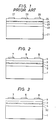
- Fig. 1 shows a sectional view of a conventional two-dimensional-electron transistor whose substrate is made of InP.
- the thickness of the GaInAs layer 23 is more than 1000 ⁇ .
- a control electrode 26 is provided in the AlInAs layer 24.
- a source electrode 27 and a drain electrode 28 are provided at both the sides of the control electrode 26.
- a two-dimensional-electron layer 25 is formed at the boundary of the GaInAs layer 23 and the n-type AlInAs layer 24 so that the field effect transistor is made up.
- the above-mentioned conventional field effect transistor has a problem that an impurity in the InP substrate 21 diffuses into the AlInAs layer 22 to make it difficult to obtain a good pinch off property of the field-effect transistor.
- the transistor has another problem that the properties thereof are likely to be affected by the substrate so that fluctuation of the property is apt to occur due to the difference between the lots of the substrates.
- an InP layer or an AlInAs layer to which a dondor impurity is added is formed on an InP substrate; a GaInAs layer to which no impurities are added is made on the InP layer or the AlInAs layer; an AlInAs layer is made on the GaInAs layer; a control electrode is provided on the AlInAs layer; and a source electrode and a drain electrode are provided at both the sides of the control electrode which make ohmic contact to the GaInAs layer.
- a two-dimensionalelectron layer is formed on the boundary between the n-type InP layer or the n-type AlInAs layer and the GaInAs layer.
- the control electrode needs to be provided in order to control the concentration of electrons in the two-dimensional-electron layer.
- the control electrode needs to make non-ohmic contact. Although Schottky contact is generally used as non-o hmic contact, it is usually difficult to make the Schottky contact to the GaInAs layer.
- the Schottky contact is not made directly to the GaInAs layer, but the AlInAs layer to which it is easy to generate non-ohmic contact is made on the GaInAs layer and the control electrode is thereafter provided on the AlInAs layer.
- An impurity either may be added to the AlInAs layer to provide the layer with the p-type or n-type of electric conduction, or may not be added thereto.
- an appropriate electric conduction type is selected for the AlInAs layer depending on the desired properties of the field effect transistor. For example, when the dielectric strength of the field effect transistor against the input voltage to the control electrode is to be enhanced, it is preferable to add no impurities to the AlInAs layer.
- the threshold voltage of the field effect transistor is to be made positive, the AlInAs layer is provided with the p-type of electric conduction.
- the AlInAs layer is provided with the n-type of electric conduction.
- the influence of an impurity which diffuses from the InP substrate is reduced.
- the concentration of the impurity which diffuses from the InP substrate is about 1016 cm ⁇ 3 and the depth of the diffusion is about 300 ⁇ . Therefore, the influence of the impurity which diffuses from the InP substrate can be reduced by making the thickness of the n-type layer and the concentration of donor impurity thereof larger than about 300 ⁇ and 1016 cm ⁇ 3,respectively.
- a first embodiment of the present invention which is a field effect transistor, is hereafter described with reference to Fig. 2.
- a first AlInAs layer 2 doped with a donor impurity is formed on a semi-insulating InP substrate 1 by an organic metal gas-phase growth method or a gas-source MBE (molecular-beam epitaxy method )at the substrate temperature of 600°C to 650°C. Si, S, Se or the like is supplied in the form of a hydride as the donor impurity.
- the concentration of the impurity and the thicknes of the first AlInAs layer 2 are set at about 1 x 10¹⁷ to 5 x 1018 cm ⁇ 3 and at 500 ⁇ to 2,000 ⁇ , respectively.
- the concentration of an impurity which diffuses from the InP substrate 1 is about 1016 cm ⁇ 3 and the depth of the diffusion is about 300 ⁇ . Therefore, the influence of the impurity which diffuses from the InP substrate 1 is almost all eliminated by making the concentration of the donor impurity and the thickness of the first AlInAs layer 2 larger than that of the diffusing impurity and the depth of the diffusion thereof, respectively.
- a GaInAs layer 3 to which no impurities are added is formed at a thickness of about 150 ⁇ to 2,000 ⁇ . It is possible to make an field effect transistor having superior amplification characteristics when the thickness of the AlInAs layer 3 is thin. However, if the thickness is less than 150 ⁇ , the density of two-dimensional electrons becomes small so that the range of gate voltage with the amplification operation becomes narrow.
- a second AlInAs layer 5 is then made at a thickness of about 200 ⁇ to 2.,000 ⁇ .
- the composition of the mixed crystal of each of the first AlInAs layer 2, the GaInAs layer 3 and the second AlInAs layer 5 is made such that the lattice mismatch thereof to the InP substrate 1 is 0.1% or less.
- An impurity either may be added to the second AlInAs layer 5 to provide the layer with the p-type or n-type of electric conduction, or may not be added thereto, depending on the desired properties of the field effect transistor. For example, when the high input withstand voltage is needed, the impurity is not added.
- the second AlInAs layer 5 is provided with the n-type of electric conduction.
- the threshold voltage is to be made positive, the layer 5 is provided with the p-type of electric conduction.
- the impurity such as Si, S and Se is added thereto at a concentration of about 1016 cm ⁇ 3 to 1018 cm ⁇ 3.
- the impurity such as Zn, Mg and Mn is added thereto at a concentration of about 1016 cm ⁇ 3 to 1018 cm ⁇ 3.
- the impurity is not added to the AlInAs layer 5
- the two-dimensional electron layer 4 is formed and a leak current between the source and the gate is decreased so that the noise of the field effect transistor can be suppressed.
- the impurity is not added to the AlInAs layer 24, the two-dimensional electron layer 25 is not formed so that the property of field effect transistor is not obtained.
- An ohmic contact metal formed of an Au-Ge alloy is evaporated and is subjected to alloying at a temperature of, for example, 400°C to make a course electrode 7 and a drain electrode 8.
- a control electrode 6 is made of Al,Pt, Au, W, WSi or the like by an evaporation method or the like, thus completing the field effect transistor.
- Fig. 3 is a sectional view showing a second embodiment of the present invention.
- the same reference numeral in Figs. 1 and 3 disignate the same parts.
- the second embodiment is identical to the first embodiment except that an n-type InP layer 32 is formed on the InP substrate 1.
- the InP layer 32 is made on the semi-insulating InP substrate 1 by the organic metal gas-phase growth method or the gas-source molecular-beam epitaxy method at the substrate temperature of 600°C to 650°C with being added by a donor impurity such as Si, S and Se. At that time, the concentration of the donor impurity and the thickness of the InP layer 32 are set at about 1 x 1017 cm ⁇ 3 to 5 x 1018 cm ⁇ 3 and at 500 ⁇ to 2,000 ⁇ , respectively.
- the GaInAs layer 3, AlInAs layer 5, control electrode 6, source electrode 7 and drain electrode 8 are formed by the same method as in the first embodiment.
- the field effect transistor of the first embodiment or the second embodiment since the n-type AlInAs layer 2 or the n-type InP layer 32 is formed on the InP substrate 1, the influence of an impurity which diffuses from the InP substrate is reduced. Accordingly, the field effect transistor having superior high-frequency property and amplifying property can be manufacturing with high reproducibility.
Landscapes
- Junction Field-Effect Transistors (AREA)
Applications Claiming Priority (4)
| Application Number | Priority Date | Filing Date | Title |
|---|---|---|---|
| JP61254180A JPS63107172A (ja) | 1986-10-24 | 1986-10-24 | 電界効果トランジスタ |
| JP254181/86 | 1986-10-24 | ||
| JP254180/86 | 1986-10-24 | ||
| JP61254181A JPS63107173A (ja) | 1986-10-24 | 1986-10-24 | 電界効果トランジスタ |
Publications (1)
| Publication Number | Publication Date |
|---|---|
| EP0264932A1 true EP0264932A1 (de) | 1988-04-27 |
Family
ID=26541567
Family Applications (1)
| Application Number | Title | Priority Date | Filing Date |
|---|---|---|---|
| EP87115444A Withdrawn EP0264932A1 (de) | 1986-10-24 | 1987-10-21 | Feldeffekttransistor |
Country Status (3)
| Country | Link |
|---|---|
| EP (1) | EP0264932A1 (de) |
| KR (1) | KR900008154B1 (de) |
| CA (1) | CA1261977A (de) |
Cited By (1)
| Publication number | Priority date | Publication date | Assignee | Title |
|---|---|---|---|---|
| US5170230A (en) * | 1989-05-10 | 1992-12-08 | Fujitsu Limited | Semiconductor device and production method thereof |
Citations (5)
| Publication number | Priority date | Publication date | Assignee | Title |
|---|---|---|---|---|
| GB2012480A (en) * | 1978-01-12 | 1979-07-25 | Plessey Co Ltd | Heterostructure field effect transistors |
| EP0050064A2 (de) * | 1980-10-14 | 1982-04-21 | Thomson-Csf | Feldeffekttransistor mit hoher Grenzfrequenz |
| EP0051271A1 (de) * | 1980-10-31 | 1982-05-12 | Hitachi, Ltd. | Halbleiteranordnung mit Heteroübergängen |
| EP0114962A2 (de) * | 1982-12-30 | 1984-08-08 | International Business Machines Corporation | Feldeffekttransistor mit doppeltem Heteroübergang |
| EP0147196A2 (de) * | 1983-12-23 | 1985-07-03 | Hitachi, Ltd. | Halbleiterelement und Halbleiteranordnung mit solchem Element |
-
1987
- 1987-10-21 EP EP87115444A patent/EP0264932A1/de not_active Withdrawn
- 1987-10-23 KR KR1019870011772A patent/KR900008154B1/ko not_active Expired
- 1987-10-23 CA CA000550121A patent/CA1261977A/en not_active Expired
Patent Citations (5)
| Publication number | Priority date | Publication date | Assignee | Title |
|---|---|---|---|---|
| GB2012480A (en) * | 1978-01-12 | 1979-07-25 | Plessey Co Ltd | Heterostructure field effect transistors |
| EP0050064A2 (de) * | 1980-10-14 | 1982-04-21 | Thomson-Csf | Feldeffekttransistor mit hoher Grenzfrequenz |
| EP0051271A1 (de) * | 1980-10-31 | 1982-05-12 | Hitachi, Ltd. | Halbleiteranordnung mit Heteroübergängen |
| EP0114962A2 (de) * | 1982-12-30 | 1984-08-08 | International Business Machines Corporation | Feldeffekttransistor mit doppeltem Heteroübergang |
| EP0147196A2 (de) * | 1983-12-23 | 1985-07-03 | Hitachi, Ltd. | Halbleiterelement und Halbleiteranordnung mit solchem Element |
Non-Patent Citations (1)
| Title |
|---|
| INTERNATIONAL ELECTRON DEVICES MEETING, TECHNICAL DIGEST, Washington, DC, 1st-4th December 1985, pages 321-323, IEEE, New York, US; K.S. SEO et al.: "DC and microwave performance of In0.53Ga0.47As-In0.52Al0.48As single quantum well MISFETS" * |
Cited By (1)
| Publication number | Priority date | Publication date | Assignee | Title |
|---|---|---|---|---|
| US5170230A (en) * | 1989-05-10 | 1992-12-08 | Fujitsu Limited | Semiconductor device and production method thereof |
Also Published As
| Publication number | Publication date |
|---|---|
| CA1261977A (en) | 1989-09-26 |
| KR880005689A (ko) | 1988-06-30 |
| KR900008154B1 (ko) | 1990-11-03 |
Similar Documents
| Publication | Publication Date | Title |
|---|---|---|
| EP0256363B1 (de) | AlGaAs/GaAs komplementäre IC-Struktur | |
| US5610410A (en) | III-V compound semiconductor device with Schottky electrode of increased barrier height | |
| US5319223A (en) | High electron mobility transistor | |
| KR920003799B1 (ko) | 반도체 장치 | |
| JPH10270467A (ja) | 半導体装置 | |
| JPH0324782B2 (de) | ||
| EP2416353A1 (de) | Halbleiterbauelement | |
| US20040266090A1 (en) | Semiconductor device and method for manufacturing semiconductor device | |
| US4866491A (en) | Heterojunction field effect transistor having gate threshold voltage capability | |
| EP0228624B1 (de) | Feldeffekttransistor | |
| US5895929A (en) | Low subthreshold leakage current HFET | |
| US5381027A (en) | Semiconductor device having a heterojunction and a two dimensional gas as an active layer | |
| US5258631A (en) | Semiconductor device having a two-dimensional electron gas as an active layer | |
| US5159414A (en) | Junction field effect transistor of a compound semiconductor | |
| USH291H (en) | Fully ion implanted junction field effect transistor | |
| JP3036404B2 (ja) | 半導体装置とその製造方法 | |
| JPH07273310A (ja) | 共振トンネリングfetおよびその製造方法 | |
| EP0264932A1 (de) | Feldeffekttransistor | |
| JPS6242569A (ja) | 電界効果型トランジスタ | |
| US5242846A (en) | Method of manufacturing a junction field effect transistor | |
| JPH09237889A (ja) | 半導体結晶積層体及びそれを用いた半導体装置 | |
| KR910006698B1 (ko) | 반도체 장치 | |
| JPH0312770B2 (de) | ||
| JP2695832B2 (ja) | ヘテロ接合型電界効果トランジスタ | |
| JPH0260224B2 (de) |
Legal Events
| Date | Code | Title | Description |
|---|---|---|---|
| PUAI | Public reference made under article 153(3) epc to a published international application that has entered the european phase |
Free format text: ORIGINAL CODE: 0009012 |
|
| AK | Designated contracting states |
Kind code of ref document: A1 Designated state(s): DE FR GB NL |
|
| 17P | Request for examination filed |
Effective date: 19880601 |
|
| 17Q | First examination report despatched |
Effective date: 19910716 |
|
| STAA | Information on the status of an ep patent application or granted ep patent |
Free format text: STATUS: THE APPLICATION IS DEEMED TO BE WITHDRAWN |
|
| 18D | Application deemed to be withdrawn |
Effective date: 19911127 |
|
| RIN1 | Information on inventor provided before grant (corrected) |
Inventor name: SASAKI, GOROC/O YOKOHAMA WORKS OF SUMITO |