EP0265698A2 - Dispositif de connexion pour la connexion électrique des branchements d'appareils électriques - Google Patents
Dispositif de connexion pour la connexion électrique des branchements d'appareils électriques Download PDFInfo
- Publication number
- EP0265698A2 EP0265698A2 EP87114294A EP87114294A EP0265698A2 EP 0265698 A2 EP0265698 A2 EP 0265698A2 EP 87114294 A EP87114294 A EP 87114294A EP 87114294 A EP87114294 A EP 87114294A EP 0265698 A2 EP0265698 A2 EP 0265698A2
- Authority
- EP
- European Patent Office
- Prior art keywords
- housing
- plug
- circuit
- connecting device
- connection
- Prior art date
- Legal status (The legal status is an assumption and is not a legal conclusion. Google has not performed a legal analysis and makes no representation as to the accuracy of the status listed.)
- Granted
Links
Images


Classifications
-
- H—ELECTRICITY
- H02—GENERATION; CONVERSION OR DISTRIBUTION OF ELECTRIC POWER
- H02B—BOARDS, SUBSTATIONS OR SWITCHING ARRANGEMENTS FOR THE SUPPLY OR DISTRIBUTION OF ELECTRIC POWER
- H02B1/00—Frameworks, boards, panels, desks, casings; Details of substations or switching arrangements
- H02B1/20—Bus-bar or other wiring layouts, e.g. in cubicles, in switchyards
- H02B1/202—Cable lay-outs
Definitions
- the invention relates to a connecting device for the electrical connection of electrical connections of electrical devices, in particular electronic devices, by means of connecting cables having plug connections according to the preamble of claim 1 and / or claim 19.
- German patent application P 35 22 710 (EP 86 107 698.2) suggests first of all to use connecting cables, at one end of which corresponding connections are provided, and the other end of which is always provided with the same type of connections , namely so-called coupling elements. Furthermore, a connector is proposed in which the respective coupling elements can be inserted on both sides, wherein an electrical connection between opposite connection ends of the contact elements is possible by means of a circuit board provided within the connector in the manner of a printed circuit (or in another way).
- the connector housing of a connector and thus also the corresponding circuit board can be designed so that more than one coupling element can be inserted.
- the circuit housing has on the one hand only plug connection elements according to a single standard, namely that which is proposed in the proposal.
- the connection to the circuit housing can be made from any device.
- the circuit housing has the circuit board which connects the two ends of the connector housing parts to one another via the plug connection elements and thus enables the electrical connection.
- the circuit board can be accommodated in the circuit housing are designed so that they can also accommodate larger circuits.
- it can accommodate actuation and / or display elements.
- the user can switch between different applications without having to change the connections between the electrical devices to be connected. These can be displayed. Other functions can also be displayed.
- a plurality of circuit housings could be connected to one another interchangeably, it also being possible to provide circuit housings which do not contain any connectors, to which no connecting cable can be connected from an electrical device.
- This will be the case if the interface circuits and / or the signal code recoding circuits require considerable effort, which makes it advisable for cost reasons (and space reasons), not all possibilities within one To provide circuit housing provided circuit.
- the basic idea of the proposal can also be used to connect such different circuit housings.
- connection can be made in such a way that the electrical connection takes place via a circuit board connecting two circuit housings, the circuit board being insertable into at least one of the circuit housings fixedly arranged coupling elements, the other ends of which are electrically connected to the circuit board arranged there, if appropriate directly to the latter are soldered on.
- This can be the case for both circuit housings.
- the design can also be such that a plug-in module is connected between two circuit housings to be coupled with one another, which has coupling elements at both ends, these being rigidly connected to one another. Electrical and / or electronic components can be present within the rigid section of the plug-in module. This enables additional additional programming or coding.
- Such programming is also possible by means of plug-in modules which can only be inserted in a circuit housing and which contain the corresponding electrical and / or electronic components.
- circuit housings can be designed to be stackable horizontally and / or vertically.
- appropriate plug-in modules can also be used for external programming in a single circuit housing, with additional security against incorrect connections being achieved by suitable training, also by covering plug-in connection elements.
- the design of the coupling elements with at least one inscribable field which is also proposed according to the application, enables the consumer to quickly identify which coupling element is to be used in his application or which connector it is to be connected to.
- the combined use of the two anmel Proposals according to the invention namely circuit housing on the one hand and labeling field on the other hand, enable an extremely consumer-friendly and, at the same time, cost-saving connection of electrical devices, in particular electronic devices, even if they have numerous poles, such as, for example, in data processing devices.
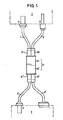
- connecting cables 1, 2 and 1 ⁇ , 2 ⁇ are provided, which are provided on one end of the cable with plug connections that correspond to the standards of the respective electrical devices Y and Z and therefore in the connections a, b and e, f can be inserted.
- the connecting cables 1 to 4 coupling elements K1, K2, K1 ⁇ or K2 ⁇ which are designed as uniform plug connections.
- a connector V which consists of two connector parts V1 ⁇ and V2 ⁇ , in which on the one hand the coupling elements K1 and K2 and on the other hand the coupling elements K1 ⁇ and K2 ⁇ can be inserted.
- the connector V contains a circuit board which is held in the two connector parts V1 ⁇ and V2 ⁇ , the two connector parts being non-detachable are connected to one another, that is to say form a unit as a whole.
- the circuit board contains conductor tracks that connect the respective contact elements of the coupling elements to one another.
- the coupling elements can have the same or different number of contact elements and the connector can be suitable for receiving one or more of the coupling elements.
- a number of contact elements of three appears expedient, which is why the connector expediently has a circuit board which has three conductor tracks or an integral multiple thereof and which has a corresponding spatial configuration.
- the circuit board of the connector accordingly has 6 conductor tracks.
- connection device can be used advantageously at least in most audio and video applications, there are difficulties, however, when a larger number of actual electrical connections have to be made and a direct electrical connection may not be readily permissible. Such use cases occur especially when it comes to electronic data processing. In particular, not all electrical connections are permitted there for reasons of compatibility.
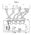
- two electrical devices Y and Z are also to be electrically connected to one another. These devices also have electrical connections a, b or c and d.
- a direct connection of the two devices to each other either in the conventional way, not permitted by the way suggested in the proposal, or to a reasonable extent not possible.
- connections c and d are very large, as is indicated schematically at connections c and d of device Y.
- multiple connections of the same type are often provided in data processing devices, the connection contacts of which are not completely occupied, and to which a corresponding application must be connected separately.
- a circuit housing X is now provided in accordance with the present invention, which contains a circuit board 11 of larger dimensions, on which a printed circuit and further electrical and / or electronic components can be accommodated.
- a circuit board 11 of larger dimensions, on which a printed circuit and further electrical and / or electronic components can be accommodated.
- an integrated circuit 35, an electrical switch 36 and an indicator lamp 37 are provided in FIG. 2.
- the actuation button 38 of the switch 36 is guided to the outside and can be actuated from the outside.
- the visible side of the display element 37 also faces outwards, as is shown.
- the housing X in its rear wall 39 has a plurality of connector housing parts Vi, of which a total of connector housing parts V1, V2, V3 and V4 are shown in the exemplary embodiment, which are each suitable for receiving two coupling elements Ki in accordance with the embodiment according to FIG. 1 .
- various connection cables with coupling elements K1 to K6 on the one hand, and corresponding pluggable connections at the other end for the electrical connection with the connections a, b, c and d of the electrical devices Z and Y to be connected to one another are provided.
- the connection cables 1 and 2 correspond in structure essentially to the connection cables 1 and 2 shown in FIG. 1.
- the connection cable 3 is only indicated and is connected together with connection cables 4 and 5 together with the connection d of the electrical device Y.
- Each of the connecting cables 4 and 5 carries a corresponding coupling element K4 or K6 at the other end.
- a multi-core connecting cable 8 is connected, which branches into cable sections 6 and 7, which carry coupling elements K5 and K3 at their ends.
- the contact elements of the various coupling elements K1 to K6 are connected to corresponding contact elements of the different connector housing parts V1 to V4, these contact elements being arranged on the circuit board 11.
- not all connection options of the connector housing parts are used. This shows that a different assignment and thus also programming is possible.
- all connections of an electrical device can be advantageously connected to the provided on the circuit board 11 printed circuit in the circuit housing X, which, by suitable design of the printed circuit and actuation of corresponding electrical switches 36, the change in the device function which was previously possible only by annoying changing of the electrical device is possible and can be displayed accordingly.
- the circuit housing X therefore expediently accommodates a plurality of such switches 36, which in turn have a plurality of switching elements which can each be actuated by a single actuation button 38.
- Such switches are commercially available. In this way, devices from different manufacturers can be connected.
- the circuit board 11 expediently contains interface circuits of two or more manufacturer standards, as well as signal code recoding circuits, in order to be able to connect the devices from different manufacturers, which are usually not compatible with one another. It is expedient if the connector housing parts Vi are arranged in a wall, namely the rear wall 39 of the circuit housing X, while actuation and display parts such as the actuation button 38 and the display element 37 are provided in the front wall 40 of the circuit housing X. Front 40 and back 39, in particular with regard to the different connector housing parts Vi, can be labeled in accordance with a system standard in order to give the consumer the assignment of the various coupling elements K1 to K6 to the individual connector housing parts V1 to V4 and the contact elements of the circuit board 11 to facilitate.
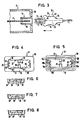
- a connector housing part V1 according to an embodiment is shown in detail.
- an embodiment is shown, which can also be used as a connector housing part V1 ⁇ or V2 ⁇ of the connector V according to the main patent.
- the housing part 10 has, on the sections and sides pointing into the interior of the circuit housing X, snap-fit or form-fitting mating and pluggable connecting parts 10a, 10a ⁇ , 10b and 10b ⁇ , via which a connection to another connector housing part would be possible, whereby, as already stated in the main patent, both housing parts V1 ⁇ and V2 ⁇ should be identical for the same reasons mentioned.
- a part of the connecting parts is raised, another is recessed, whereby, as explained in the main patent, they are designed so that they engage and lock together when plugged together.
- other embodiments are also possible.
- each housing part 10 has on both sides of the rectangular hollow housing section a pair of guide lugs 22 for guiding the respective section of the circuit board 11 (see FIG. 2) in the center of the cavity 23 of the housing part 10.
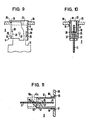
- the circuit board 11 according to FIG. 2
- the circuit board 11 can (see FIG. 9) have a stop projection 24 on the tongue 9 which strikes a stop 25 when the circuit board 11 is inserted into the housing part 10.
- latching knobs 26 latch in the housing part 10 via their projecting ends in a latching opening 27 in the tongue 9 of the circuit board 11.
- Each connector housing part V1 to V4 is assigned at least one such latching knob / latching opening connection, as is particularly the case in FIG. 10 is recognizable at the end of assembly.
- the tongue 9 of the patine 11 has locking shoulders 28 which lock behind locking cams 29.
- each housing part 10 has a respective guide groove 32 on the opposite walls of the respective cavities 30, 31, which are arranged eccentrically to the cavity axes.
- These guide grooves 32 basically correspond to guide grooves, as are explained in the housing parts according to the proposal, and which interact with corresponding guide elements on the coupling elements.
- coding ribs 33 can be formed in a different geometric arrangement, which cooperate with corresponding coding elements or coding grooves in the coupling elements for the purpose of unmistakably plugging the connector plug-in connection (contact element) and the corresponding coupling element.
- the different geometric arrangement can be caused by the height, the width, the shape and / or the number of the coding ribs 33 used.
- the geometric arrangement can be such that a plurality of differently coded coupling elements can be inserted into a cavity in the manner of a superordinate and subordinate arrangement, or vice versa, a coupling element having a specific coding can be inserted into several differently coded cavities.
- the housing 10 can have latching lugs 19 on the outside. As a result, the housing part 10 can be securely fixed in the rear wall 39.
- the housing part 10 is inserted from the outside of the circuit housing X through a correspondingly dimensioned opening 18 such that the latching lug 19 engages behind the rear wall 39, while the raised peripheral edge 20 rests on the outside or in a corresponding recess 17 (FIG. 11 ) intervenes.
- Fig. 11 shows another embodiment of the locking connection between the housing part 10 and the circuit board 11 or its tongue 9.
- a tab 41 protrudes from the housing part 10 to the rear and has a corresponding locking knob 26a at the extreme end, which in a corresponding latching opening 27a of the tongue 9 engages.
- this embodiment is also fundamentally applicable to the connecting device according to the proposal, since the other housing part 10a can also be designed in a corresponding manner with a fin-like extension 21a with latching knobs 26, which then engages in a latching opening 27 in the tongue 9.
- the illustration shows that even complete compatibility (see FIG. 9) can be achieved here.
- several such approaches 41 and 41a can also be arranged next to one another.
- the fin-like approach can have a support section 42 for the tongue 9 of the circuit board 11 between the connection to the housing part 10 and the locking knobs 26a, as a result of which better support is achieved (a reinforced clamping effect being achieved with a connector V as proposed).
- the coupling element Ki has a coupling housing 13 made of insulating material, which has a continuous slot 14 on the front. With spring spacing to the inner surfaces of the slot 14 there are fork-shaped contact ends of contact springs 15, the free ends of the contact springs 15 have contact tips 12. At the non-free end, an extension 16 protrudes from the coupling housing 13 to which a wire or a shield of the cable i is soldered . In this area, the coupling housing 13 of the coupling element Ki is surrounded by an insulating sleeve 43, which is preferably produced by extrusion coating is.
- This insulating sleeve 43 encloses a part of the coupling housing 13 and in particular the soldering point on the attachment 16.
- the coupling housing 13 has the corresponding guide ribs or grooves and / or coding ribs or grooves on its surfaces pointing upwards or downwards (FIG. 3) as explained above for the housing 10.
- the guide grooves on the clutch housing 13 and the corresponding guide ribs on the housing part 10 can be provided and vice versa.
- Contact springs 15 arranged laterally next to one another in the coding housing 13 are preferably spaced apart from one another in accordance with the grid dimension of 2.5 mm customary in printed circuits.
- FIG. 12 shows an embodiment in which an additional circuit housing X ⁇ is provided in addition to the circuit housing X.
- Both circuit housings X and X ⁇ basically have the same embodiment, they contain a circuit board 11 or 11 ⁇ to which corresponding coupling elements (not shown here) can be connected via housing parts 10 and 10 ⁇ .
- supports 44 and 45 can be provided in the housings as shown for the circuit housing X to support the circuit board 11.
- Fig. 12 shows an embodiment in which the housings X and X ⁇ are vertically stackable, namely in that they are placed on top of each other. A similar design is also shown in FIG. 13.
- coupling housing 13 can be soldered into the respective printed circuit of the circuit board 11 or 11 ⁇ via its unfree ends 16.
- the respective plug-in slots lie opposite one another via aligned housing openings 46 and 47.
- the electrical connection is made with the aid of a printed circuit board 48, which can have the structure of the circuit board according to the proposal, in such a way that the electrical connection takes place in the two coupling housings 13 via the resilient contact of the contact tips 12 of the contact springs 15.
- FIG. 13 shows an exemplary embodiment in which a circuit board 13 is assigned a circuit board 48 which projects through the opening 46 of the circuit housing X. Furthermore, a second U-shaped circuit board 50 is assigned to two coupling housings 13 arranged next to one another, and projects outward from the circuit housing X via a correspondingly dimensioned housing opening 49.
- the circuit board 50 on the outwardly projecting side two tongues 51 and 52.
- a coupling housing 13 was assigned to both boards 11 and 11 ⁇ .
- a plurality of circuit boards which are electrically connected to one another can also be arranged in a housing X.
- 14 shows the circuit board 11 and an additional circuit board 61.
- the circuit board X of the circuit housing X according to FIG. 14, like the circuit board 11, has tongues 59 which, similar to the housing part 10, protrude into a corresponding housing part 60, which expediently has the same design as the housing part 10.
- the connection of the printed circuits of the two boards 11 and 61 can take place within the housing X. However, external programming of your choice is possible using a plug-in module 58.
- the plug-in module 58 has coupling housings 13 of the type described at both ends, by means of which an electrical connection to the conductor tracks on the tongues 59 and 9 of the two boards 61 and 11 is possible.
- the plug-in module 58 namely the essentially rigid connection Section 57 is at least a direct electrical connection, coding being possible if desired.
- the connecting section 57 can also contain electrical and / or electronic components, the same design options being basically available as are explained for the coupling elements according to the main patent with regard to coding and guidance and the number of contact springs arranged next to one another.
- plug-in module 58 With a correspondingly dimensioned plug-in module 58, it is also possible to connect the boards 11 and 11 ⁇ of two vertically stacked housings X and X ⁇ , cf. Fig. 12, achieve that are then to be inserted into the corresponding housing parts 10 and 10 ⁇ .
- Coding by means of a plug-in module is also possible in the case of a circuit housing X with a single circuit board 11, such a plug-in module 62, which internally has a schematically indicated electrical circuit 63, only having a single coupling housing 13 which is inserted into a housing part 10 for contacting the conductor tracks is provided on the corresponding tongue 9 of the board 11.
- coding and / or programming can take place by appropriate selection of the plug-in module 62, such as a termination with a certain resistance, a short circuit or the like.
- circuit housings X and X ⁇ can be connected to one another by means of a plug-in module 64.
- This plug-in module 64 also has coupling housings 13 at the ends, which are provided for contacting the conductor tracks of the circuit board 11 in the circuit housing X or the circuit board 65 in the circuit housing X ⁇ .
- the connecting section 66 can, like the connecting section 57 of the plug-in module 58 according to FIG. 14 only lines or conductor tracks, if necessary, but also contain additional electronic components for coding and / or programming. As explained with reference to FIG.
- a housing part 67 is also provided in the circuit housing X ⁇ , which receives a corresponding tongue 68 of the circuit board 65 and into which the one coupling housing 13 can be inserted.
- the described guide and / or coding grooves or ribs can also be provided here.
- FIG. 17 Another embodiment is shown in FIG. 17.
- coding and / or programming e.g. a change in function achieved in the circuit on the circuit board 11 of the circuit housing X.
- two coupling housings 13 are likewise provided at the ends, the design being such that, when inserted in the corresponding housing parts 10, certain cavities (cf. FIG. 4) of the housing parts 10 are no longer accessible. This can prevent a malfunction when programming is selected.
- more than two such coupling housings 13 can also be provided on a plug-in module.
- plug-in modules are possible, for example any combinations of the plug-in modules 58, 62, 64, 69 explained.
- the housing parts 10 can have an outer shell 71, a metal foil 73 which achieves a metallic shielding being able to be provided between this shell 71 and the housing wall 72, as already explained in the proposal is.
- the shielding is expedient 73 electrically connected to the circuit board 11 or the conductor tracks, the electrical tongue 9 thereof, the connection being able to take place, for example, via the locking knobs 26, as is explained in the proposal, for which purpose this has an electrically conductive coating or the like.
- the electrical shielding can also be provided by an electrically conductive plastic that is insulated from the outside.
- shielding is often provided in principle in the applications in question, namely, shielded cores are used, it may be expedient to assign a contact spring to each coupling element 13 of the shield, the corresponding connection of the tongue 9 of the circuit board being assigned the corresponding connection to the shield 73 is
- the insulating sleeve 43 can have cross ribs 74, 75 which facilitate handling. Furthermore, lettering and / or marking can be provided on the side surfaces 76, this lettering and / or marking being able to be applied positively or negatively during the spraying process by suitable formation of the spray mold.
- a comparable design of a coupling element Ki ⁇ shows Fig. 18 and Fig. 19. It is essential in the embodiment according to FIG. 18 that in addition a strain relief 77 for the cable i is injection molded simultaneously with the insulating sleeve 43 ⁇ . Furthermore, the insulating sleeve 43 79 according to FIG.
- 18 has additional fields 78, 79 which are provided for inscription and which are also visible when plugged in and when a plurality of similar coupling elements Ki ⁇ are arranged next to one another.
- the inscription can be molded on in the same way, it can also be done in addition.
- 19 indicates that the coupling element need not only have a coupling housing 13, As has already been explained, but as indicated by dashed lines, a clutch housing 13 ⁇ can have a larger width, the total width of the clutch housing 13 ⁇ expediently corresponding to an integer multiple of the width of the clutch housing 13.
- Such training allows the fixed connection of several cables i with a one-piece coupling element Ki ⁇ .
- a strain relief 77 can be provided for each of the cables i, and gripping grooves 74 ⁇ , 75 ⁇ can also be provided in the same way as was explained above with reference to FIG. 3.
- differently colored plastics can also be used for the coupling housing 13 and / or the insulating sleeves 43 and 43 ⁇ .
- a system which is universally suitable for connecting a wide variety of electrical and electronic devices.
- the system is designed in such a way that any simple electrical connection is possible on the basis of simple components for the connection, even with comparatively complicated devices from a wide variety of manufacturers, such as data processing devices.
- This connecting device is therefore particularly suitable for standardization, especially since the coding and programming options are almost unlimited are and can be safely avoided for the devices even harmful exchanges.
- the system according to the application is suitable for systematization with regard to all applications, in such a way that even users without special previous knowledge can achieve the desired electrical connections. All in all, a complete and compatible bus system can be created that is not only commercial, but also professionally applicable and allows smooth transitions as desired by the user.
Landscapes
- Engineering & Computer Science (AREA)
- Power Engineering (AREA)
- Coupling Device And Connection With Printed Circuit (AREA)
- Details Of Connecting Devices For Male And Female Coupling (AREA)
- Testing Of Short-Circuits, Discontinuities, Leakage, Or Incorrect Line Connections (AREA)
Applications Claiming Priority (2)
| Application Number | Priority Date | Filing Date | Title |
|---|---|---|---|
| DE3633218 | 1986-09-30 | ||
| DE19863633218 DE3633218A1 (de) | 1985-06-25 | 1986-09-30 | Verbindungsvorrichtung fuer die elektrische verbindung von elektrischen anschluessen von elektrogeraeten |
Publications (3)
| Publication Number | Publication Date |
|---|---|
| EP0265698A2 true EP0265698A2 (fr) | 1988-05-04 |
| EP0265698A3 EP0265698A3 (en) | 1989-04-12 |
| EP0265698B1 EP0265698B1 (fr) | 1994-03-30 |
Family
ID=6310688
Family Applications (1)
| Application Number | Title | Priority Date | Filing Date |
|---|---|---|---|
| EP87114294A Expired - Lifetime EP0265698B1 (fr) | 1986-09-30 | 1987-09-30 | Dispositif de connexion pour la connexion électrique des branchements d'appareils électriques |
Country Status (4)
| Country | Link |
|---|---|
| US (1) | US4981438A (fr) |
| EP (1) | EP0265698B1 (fr) |
| JP (1) | JPS63158774A (fr) |
| AT (1) | ATE103739T1 (fr) |
Families Citing this family (39)
| Publication number | Priority date | Publication date | Assignee | Title |
|---|---|---|---|---|
| US5108294A (en) * | 1990-07-25 | 1992-04-28 | Amp Incorporated | Terminator connector |
| US5187645A (en) * | 1991-06-07 | 1993-02-16 | Ergo Computing, Inc. | Portable computer with docking connector for peripheral devices |
| GB2288922B (en) * | 1994-04-25 | 1998-04-01 | John Edward Mcgrath | Patient monitoring apparatus |
| US5828905A (en) * | 1995-11-13 | 1998-10-27 | Mitsubishi Chemical America, Inc. | Adapter and method of connecting devices associated with at least three different protocols |
| US5645434A (en) * | 1995-12-01 | 1997-07-08 | Asante Technologies, Inc. | Connector element and component arrangement for a stackable communications network hub |
| US6042390A (en) * | 1995-12-01 | 2000-03-28 | Asante Technologies, Inc. | Network hub interconnection component |
| JPH10208830A (ja) * | 1997-01-20 | 1998-08-07 | Sony Corp | コネクタ用アダプタおよびコネクタ |
| US5800186A (en) * | 1997-03-13 | 1998-09-01 | Framatome Connectors Usa, Inc. | Printed circuit board assembly |
| US5984716A (en) * | 1997-06-09 | 1999-11-16 | Progressive Components International Corporation | Electrical connection system for mold components and a plastic injection molding press |
| US6511327B1 (en) * | 1997-09-29 | 2003-01-28 | Avaya Technology Corp. | Simplified network interface device |
| US6152778A (en) * | 1998-02-26 | 2000-11-28 | Hewlett-Packard Company | Electronic connector adapter with power input |
| JP3703665B2 (ja) * | 1999-11-16 | 2005-10-05 | ヒロセ電機株式会社 | 電気コネクタ接続構造 |
| US6283789B1 (en) * | 2000-03-16 | 2001-09-04 | Shui Chuan Tsai | Data and power transmitting cable system |
| TW476902B (en) * | 2000-05-19 | 2002-02-21 | Acer Inc | Universal serial bus hub |
| AU2002350212A1 (en) * | 2001-11-20 | 2003-06-10 | Dana Farber Cancer Institute | Pharmaceutically active compounds and methods of use thereof |
| DE20219377U1 (de) * | 2002-12-09 | 2003-03-06 | Siemens AG, 80333 München | Leiterplatte mit Steckeranschluss |
| US20050023026A1 (en) * | 2003-07-28 | 2005-02-03 | Wilson Chen | Network cable |
| US20060011368A1 (en) * | 2004-03-19 | 2006-01-19 | Hiroyuki Maruyama | Transfer center |
| US20050205278A1 (en) * | 2004-03-19 | 2005-09-22 | Hiroyuki Maruyama | Cable system to exchange data |
| US7121850B2 (en) * | 2004-11-05 | 2006-10-17 | Ming-Hsiang Yeh | Dual-purpose male/female connector |
| US7255577B2 (en) * | 2005-04-14 | 2007-08-14 | International Business Machines Corporation | Protective cover for DIMM circuit card |
| US20070279895A1 (en) * | 2005-05-12 | 2007-12-06 | Finelite | Workspace lighting system |
| US20070020980A1 (en) * | 2005-07-25 | 2007-01-25 | Seibert Gregory L | Electrical connection apparatus |
| WO2007133611A2 (fr) * | 2006-05-10 | 2007-11-22 | Finelite | Système d'éclairage d'un espace de travail |
| JP4505477B2 (ja) * | 2007-03-30 | 2010-07-21 | オリンパスメディカルシステムズ株式会社 | 筐体機構とこれを適用した医療用観測装置 |
| US8221152B2 (en) * | 2007-04-11 | 2012-07-17 | Hewlett-Packard Development Company, L.P. | Cable management system and method |
| US20100168547A1 (en) * | 2008-12-29 | 2010-07-01 | David Kendricks | Universal din leadwire system for use with ekg and ecg patient monitoring and event recording instruments |
| US9847636B2 (en) | 2012-10-03 | 2017-12-19 | Ideal Industries, Inc. | Low voltage buss system |
| US8485831B2 (en) * | 2011-01-06 | 2013-07-16 | International Business Machines Corporation | Tall mezzanine connector |
| CN102882085A (zh) * | 2011-07-15 | 2013-01-16 | 鸿富锦精密工业(深圳)有限公司 | 线缆连接器 |
| TWM445798U (zh) * | 2012-07-02 | 2013-01-21 | Nai-Chien Chang | 具有雙面接觸式連接器的傳輸線(二) |
| US9912100B2 (en) | 2012-10-03 | 2018-03-06 | Ideal Industries, Inc. | Low voltage buss system |
| US10186801B2 (en) | 2012-10-03 | 2019-01-22 | Ideal Industries, Inc. | Low voltage buss system |
| US9455540B2 (en) * | 2015-01-19 | 2016-09-27 | Aimmet Industrial Co., Ltd. | High-speed signal transmission device |
| US10283885B2 (en) * | 2015-11-06 | 2019-05-07 | Foxconn Interconnect Technology Limited | Electrical connector assembly and system using the same |
| DE102016224705A1 (de) * | 2016-12-12 | 2018-06-14 | BSH Hausgeräte GmbH | Elektrogerät mit verteilten elektrischen Einrichtungen |
| US11171438B2 (en) * | 2020-04-09 | 2021-11-09 | Energy Services LLC | Unitized cable plug array for mobile power generation equipment |
| CN114914739A (zh) * | 2021-02-09 | 2022-08-16 | 哈廷电子有限公司及两合公司 | 用于连接器的嵌件 |
| CN118474992A (zh) * | 2024-06-04 | 2024-08-09 | 深圳欧陆通电子股份有限公司 | 电路板连接结构、服务器电源及服务器供电系统 |
Family Cites Families (28)
| Publication number | Priority date | Publication date | Assignee | Title |
|---|---|---|---|---|
| US1779924A (en) * | 1927-11-17 | 1930-10-28 | Charles H Wallace | Junction-box outlet |
| US3524198A (en) * | 1968-02-29 | 1970-08-11 | Heath Co | Modular unit for making plug-in electrical connections |
| US3521220A (en) * | 1968-06-10 | 1970-07-21 | Black & Decker Mfg Co | Integral plug and strain relief cord set and method of manufacture |
| US3541396A (en) * | 1969-01-16 | 1970-11-17 | Ibm | Support frames for planar circuit boards |
| BE757345A (fr) * | 1969-10-17 | 1971-04-09 | Amp Inc | Boite a fusibles |
| DE1957847A1 (de) * | 1969-11-18 | 1971-05-27 | Licentia Gmbh | Elektrische Steckverbindung mit einem Stecker nach Art einer gedruckten Schaltung |
| US3654586A (en) * | 1970-03-20 | 1972-04-04 | Anderson Power Products | Indexing means for electrical connectors |
| US3668476A (en) * | 1970-09-11 | 1972-06-06 | Seeburg Corp | Self-locking enclosure for electronic circuitry and method of assembling the same |
| US3950058A (en) * | 1973-11-05 | 1976-04-13 | Lockheed Aircraft Corporation | Programmable wiring system and junction box for use therein |
| CH576709A5 (fr) * | 1974-12-06 | 1976-06-15 | Celio Tino | |
| DE2640233C3 (de) * | 1976-09-07 | 1980-10-23 | Siemens Ag, 1000 Berlin Und 8000 Muenchen | Kabelstecker für eine Vielzahl von Schaltdrähten |
| US4146287A (en) * | 1977-10-07 | 1979-03-27 | National Service Industries, Inc. | Lighting and power system and connectors therefor |
| US4280062A (en) * | 1979-08-22 | 1981-07-21 | Douglas Dynamics Inc. | Auxiliary light wiring harness |
| DE2943787A1 (de) * | 1979-10-30 | 1981-05-14 | Siemens AG, 1000 Berlin und 8000 München | Steckerkupplung |
| US4362905A (en) * | 1980-01-29 | 1982-12-07 | Nassar Ismail | Universal adapters for modular plug telephones |
| DE3133810A1 (de) * | 1981-08-25 | 1983-03-17 | Dr.-Ing. Sieger Electronic GmbH, 1000 Berlin | Adapter fuer elektronische geraete mit unterschiedlichen anschlussbuchsen |
| JPS5836585U (ja) * | 1981-09-03 | 1983-03-09 | 第一電子工業株式会社 | 電気コネクタ |
| US4440463A (en) * | 1981-10-26 | 1984-04-03 | The Bendix Corporation | Electrical connector having a metallized plastic grounding insert |
| JPS58111281A (ja) * | 1981-12-25 | 1983-07-02 | 本田技研工業株式会社 | カプラ−接続装置 |
| US4498716A (en) * | 1982-04-01 | 1985-02-12 | Ward Marvin W | Data monitoring connector for testing transmission links |
| DE8212541U1 (de) * | 1982-04-30 | 1982-08-19 | Siemens AG, 1000 Berlin und 8000 München | Interne Anschlußleitung |
| GB2139017A (en) * | 1983-04-30 | 1984-10-31 | Michael Anthony Thomas | A modular interconnector |
| US4514028A (en) * | 1983-05-09 | 1985-04-30 | Kuo Wei H | CRT updated method and apparatus for identifying integrated circuit pins |
| US4531176A (en) * | 1983-06-27 | 1985-07-23 | At&T Bell Laboratories | Cartridge having improved electrostatic discharge protection |
| US4760375A (en) * | 1983-10-28 | 1988-07-26 | Josef Stecker | Data transmission cable |
| FR2580136B1 (fr) * | 1985-04-05 | 1988-10-14 | Radiotechnique Compelec | |
| DE3539137A1 (de) * | 1985-06-25 | 1987-05-07 | Fauzi Bekhiet | Verbindungsvorrichtung fuer unterhaltungselektronik um niederfrequenz-anschluesse miteinander zu verbinden |
| FR2593085B1 (fr) * | 1986-01-23 | 1990-10-26 | Hauville Francois | Table de laboratoire. |
-
1987
- 1987-09-30 AT AT87114294T patent/ATE103739T1/de not_active IP Right Cessation
- 1987-09-30 EP EP87114294A patent/EP0265698B1/fr not_active Expired - Lifetime
- 1987-09-30 JP JP62247774A patent/JPS63158774A/ja active Pending
-
1989
- 1989-06-02 US US07/361,754 patent/US4981438A/en not_active Expired - Fee Related
Also Published As
| Publication number | Publication date |
|---|---|
| US4981438A (en) | 1991-01-01 |
| EP0265698A3 (en) | 1989-04-12 |
| EP0265698B1 (fr) | 1994-03-30 |
| JPS63158774A (ja) | 1988-07-01 |
| ATE103739T1 (de) | 1994-04-15 |
Similar Documents
| Publication | Publication Date | Title |
|---|---|---|
| EP0265698B1 (fr) | Dispositif de connexion pour la connexion électrique des branchements d'appareils électriques | |
| EP0617487B1 (fr) | Assemblage de connecteur, notamment pour un téléphone mobile | |
| DE69502190T2 (de) | Datenübertragungsverbinder | |
| DE10045498A1 (de) | Elektrische Reihenklemme | |
| EP3323176B1 (fr) | Système de connexion avec codage | |
| EP1959523A1 (fr) | Dispositif de codage pour connecteur à fiches | |
| DE202006006659U1 (de) | Elektrisches oder elektronisches Gerät | |
| DE2405464A1 (de) | Vielfachsteckverbinder zur herstellung mehrerer elektrischer verbindungen | |
| DE3545186C2 (fr) | ||
| DE2712723A1 (de) | Elektrischer verteiler | |
| EP0209691B1 (fr) | Dispositif d'interconnexion électrique pour postes de travail | |
| DE3633218A1 (de) | Verbindungsvorrichtung fuer die elektrische verbindung von elektrischen anschluessen von elektrogeraeten | |
| DE3641153A1 (de) | Mobile mehrfachschutzkontaktsteckdosenleiste | |
| WO2020192836A1 (fr) | Connecteur enfichable | |
| DE9401974U1 (de) | Adapter für den Anschluß von Telekommunikations-Endgeräten | |
| DE19525801A1 (de) | Vorrichtung zum elektrisch leitenden Verbinden von zwei elektrischen Leitungen | |
| DE4345217C2 (de) | Anschlußkabel zur Bildung einer Anschlußeinrichtung für ein Datennetz | |
| DE19615015A1 (de) | Verbindungsvorrichtung | |
| BE1025765B1 (de) | Baukastensystem zum Herstellen eines Elektronikgeräts | |
| DE202017000474U1 (de) | Gehäuse für ein elektronisches Gerät mit einer Leiterplatte | |
| CH690701A5 (de) | Mehrpoliger elektrischer Stecker. | |
| DE1690247A1 (de) | Steckverbinder zur elektrischen Verbindung mehrerer plattenfoermiger Leitungstraeger | |
| DE19715436C2 (de) | Anordnung mit einer elektrischen Verteilervorrichtung | |
| DE1590002C (de) | Elektrische Steckvorrichtung | |
| DE3818461C2 (de) | Steckerbrücke für einen zweipoligen elektrischen Gerätestecker mit einem Phasenstift, einem Nulleiterstift und einem Entriegelungsstift |
Legal Events
| Date | Code | Title | Description |
|---|---|---|---|
| PUAI | Public reference made under article 153(3) epc to a published international application that has entered the european phase |
Free format text: ORIGINAL CODE: 0009012 |
|
| AK | Designated contracting states |
Kind code of ref document: A2 Designated state(s): AT BE CH DE ES FR GB GR IT LI NL SE |
|
| PUAL | Search report despatched |
Free format text: ORIGINAL CODE: 0009013 |
|
| AK | Designated contracting states |
Kind code of ref document: A3 Designated state(s): AT BE CH DE ES FR GB GR IT LI NL SE |
|
| 17P | Request for examination filed |
Effective date: 19891005 |
|
| 17Q | First examination report despatched |
Effective date: 19910724 |
|
| GRAA | (expected) grant |
Free format text: ORIGINAL CODE: 0009210 |
|
| AK | Designated contracting states |
Kind code of ref document: B1 Designated state(s): AT BE CH DE ES FR GB GR IT LI NL SE |
|
| PG25 | Lapsed in a contracting state [announced via postgrant information from national office to epo] |
Ref country code: IT Free format text: LAPSE BECAUSE OF FAILURE TO SUBMIT A TRANSLATION OF THE DESCRIPTION OR TO PAY THE FEE WITHIN THE PRE;WARNING: LAPSES OF ITALIAN PATENTS WITH EFFECTIVE DATE BEFORE 2007 MAY HAVE OCCURRED AT ANY TIME BEFORE 2007. THE CORRECT EFFECTIVE DATE MAY BE DIFFERENT FROM THE ONE RECORDED.SCRIBED TIME-LIMIT Effective date: 19940330 Ref country code: GB Effective date: 19940330 Ref country code: BE Effective date: 19940330 Ref country code: FR Effective date: 19940330 Ref country code: SE Free format text: THE PATENT HAS BEEN ANNULLED BY A DECISION OF A NATIONAL AUTHORITY Effective date: 19940330 Ref country code: NL Effective date: 19940330 Ref country code: GR Free format text: LAPSE BECAUSE OF FAILURE TO SUBMIT A TRANSLATION OF THE DESCRIPTION OR TO PAY THE FEE WITHIN THE PRESCRIBED TIME-LIMIT Effective date: 19940330 |
|
| REF | Corresponds to: |
Ref document number: 103739 Country of ref document: AT Date of ref document: 19940415 Kind code of ref document: T |
|
| REF | Corresponds to: |
Ref document number: 3789486 Country of ref document: DE Date of ref document: 19940505 |
|
| PG25 | Lapsed in a contracting state [announced via postgrant information from national office to epo] |
Ref country code: ES Free format text: LAPSE BECAUSE OF FAILURE TO SUBMIT A TRANSLATION OF THE DESCRIPTION OR TO PAY THE FEE WITHIN THE PRESCRIBED TIME-LIMIT Effective date: 19940711 |
|
| EN | Fr: translation not filed | ||
| NLV1 | Nl: lapsed or annulled due to failure to fulfill the requirements of art. 29p and 29m of the patents act | ||
| PG25 | Lapsed in a contracting state [announced via postgrant information from national office to epo] |
Ref country code: LI Effective date: 19940930 Ref country code: CH Effective date: 19940930 Ref country code: AT Effective date: 19940930 |
|
| GBV | Gb: ep patent (uk) treated as always having been void in accordance with gb section 77(7)/1977 [no translation filed] |
Effective date: 19940330 |
|
| PLBE | No opposition filed within time limit |
Free format text: ORIGINAL CODE: 0009261 |
|
| STAA | Information on the status of an ep patent application or granted ep patent |
Free format text: STATUS: NO OPPOSITION FILED WITHIN TIME LIMIT |
|
| 26N | No opposition filed | ||
| REG | Reference to a national code |
Ref country code: CH Ref legal event code: PL |
|
| PG25 | Lapsed in a contracting state [announced via postgrant information from national office to epo] |
Ref country code: DE Effective date: 19950601 |