EP0265948B1 - Processeur de données capable de calculer immédiatement l'adresse de branchement dans un branchement à adresse relative - Google Patents
Processeur de données capable de calculer immédiatement l'adresse de branchement dans un branchement à adresse relative Download PDFInfo
- Publication number
- EP0265948B1 EP0265948B1 EP87115910A EP87115910A EP0265948B1 EP 0265948 B1 EP0265948 B1 EP 0265948B1 EP 87115910 A EP87115910 A EP 87115910A EP 87115910 A EP87115910 A EP 87115910A EP 0265948 B1 EP0265948 B1 EP 0265948B1
- Authority
- EP
- European Patent Office
- Prior art keywords
- address
- signal
- instruction
- branch
- input
- Prior art date
- Legal status (The legal status is an assumption and is not a legal conclusion. Google has not performed a legal analysis and makes no representation as to the accuracy of the status listed.)
- Expired - Lifetime
Links
Images

Classifications
-
- G—PHYSICS
- G06—COMPUTING OR CALCULATING; COUNTING
- G06F—ELECTRIC DIGITAL DATA PROCESSING
- G06F9/00—Arrangements for program control, e.g. control units
- G06F9/06—Arrangements for program control, e.g. control units using stored programs, i.e. using an internal store of processing equipment to receive or retain programs
- G06F9/30—Arrangements for executing machine instructions, e.g. instruction decode
- G06F9/32—Address formation of the next instruction, e.g. by incrementing the instruction counter
- G06F9/322—Address formation of the next instruction, e.g. by incrementing the instruction counter for non-sequential address
- G06F9/324—Address formation of the next instruction, e.g. by incrementing the instruction counter for non-sequential address using program counter relative addressing
-
- G—PHYSICS
- G06—COMPUTING OR CALCULATING; COUNTING
- G06F—ELECTRIC DIGITAL DATA PROCESSING
- G06F9/00—Arrangements for program control, e.g. control units
- G06F9/06—Arrangements for program control, e.g. control units using stored programs, i.e. using an internal store of processing equipment to receive or retain programs
- G06F9/30—Arrangements for executing machine instructions, e.g. instruction decode
- G06F9/32—Address formation of the next instruction, e.g. by incrementing the instruction counter
- G06F9/321—Program or instruction counter, e.g. incrementing
-
- G—PHYSICS
- G06—COMPUTING OR CALCULATING; COUNTING
- G06F—ELECTRIC DIGITAL DATA PROCESSING
- G06F9/00—Arrangements for program control, e.g. control units
- G06F9/06—Arrangements for program control, e.g. control units using stored programs, i.e. using an internal store of processing equipment to receive or retain programs
- G06F9/30—Arrangements for executing machine instructions, e.g. instruction decode
- G06F9/32—Address formation of the next instruction, e.g. by incrementing the instruction counter
- G06F9/322—Address formation of the next instruction, e.g. by incrementing the instruction counter for non-sequential address
Definitions
- the present invention relates to a stored program type digital computer, and more specifically, to a data processor for use in small sized digital computers such as microcomputers.
- the stored program digital computers have been adapted to fetch necessary instructions and data from an associated memory so as to execute necessary operation.
- a program counter is widely used as means for designating the address of instructions to be read out of the memory. Namely each time one instruction is executed, the program counter is incremented to designate the address of an instruction to be executed next, so that a sequence of instructions are read in accordance with the address indicated by the program counter.
- a so-called branch instruction is required.
- the branch instruction is divided into an absolute address branch instruction and a relative address branch instruction.
- Most of small scaled microcomputers of an initial stage had been operated with only the absolute address branch instructions.
- a first reason for this is that the microcomputers of the initial stage can handle only jobs of several kilobytes or less in the amount of programs, and therefore, use of the absolute address branch had not so given a trouble in development of programs.
- the branch instruction should be the relative address branch instruction.
- the relative address branch instruction has been executed by calculating the branch address by use of an arithmetic and logic unit for data processing, and then by setting the calculated branch address to the program counter.
- the address information for memory access has a bit length larger than that of the data processed in the microcomputer. Therefore, the arithmetic and logic unit cannot calculate the destination address of the relative address branch at only one operation. Therefore, a plurality of operations must be executed. This is one hindrance in a high speed operation of the computer.
- the branch destination addresses distribute in a limited range near to the current address, and it is a rare case that the branch destination addresses distribute in a wide range accessible by the microcomputer. This means that it is sufficient if the microcomputer has a function of branching to an address contained in a limited range in the case of the relative address branch instruction.
- a technique for high speed processing of relative jump instructions is disclosed in IBM technical disclosure bulletin, vol. 20, No. 4, September 1977, pages 1284-1285.
- the assembler calculates the lowest four bits of the destination address and inserts them into the instruction instead of the actual displacement, and depending from the jump direction and a comparison of the said lowest four bits of the destination address with the lowest four bits of the programm counter the remaining twelve bits are either incremented or decremented. Increment is conducted by a ordinary 16-bit increment logic, and decrement is conducted by using a 8-bit ALU and an additional four bit decrementer.
- Another object of the present invention is to provide a data processor capable of calculating a branch destination address of a relative address branch at a high speed and with a simple additional circuit.
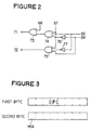
- a data processor in accordance with the present invention comprises an address bus 10 used for transmitting an address information for access to a memory 12 coupled to the address bus 10.
- the address bus 10 is of a parallel type having a width of 16 bits.
- the memory 12 is also coupled to a data bus 20 used for transferring various items of data within the computer.
- the data bus 20 is of a parallel type having a width of 8 bits.
- a pair of instruction address registers 30 and 31 of 8 bits are coupled at their outputs to the data bus 20. Further, a pair of incrementer/decrementers 40 and 41 of 8 bits are coupled at their one inputs to the data bus 20 and at their other inputs to the outputs of the instruction address registers 30 and 31, respectively. Outputs of the incrementer/decrementers 40 and 41 are coupled to respective inputs of a pair of address latches 50 and 51 of 8 bits, respectively. These address latches 50 and 51 are coupled at their outputs to the less significant 8 bits and the more significant 8 bits of the address bus 10, respectively, and also to inputs of the instruction address registers 30 and 31, respectively.
- the shown data processor includes an arithmetic and logic unit (ALU) 60 having a pair of 8-bit inputs coupled to outputs of a pair of input temporary registers 61 and 62 of 8 bits, which are in turn coupled at their inputs to the data bus 20.
- the ALU 60 has an 8-bit output coupled to an input of an output temporary register 63 of 8 bits, whose output is coupled to the data bus 20.
- the most significant bit (MSB) 64 of the temporary register 61 is supplied to a control circuit 70, which also receive a carry signal 65 from the ALU 60, another carry signal 66 from the incrementer/decrementer 40, and a control signal 67 indicative of a relative address branch instruction.
- the control circuit 70 is adapted to respond to the above four signals to generate an increment signal 71 or a decrement signal 72 to the incrementer/decrementer 41.
- the instruction address registers 30 and 31 store the address of an instruction stored in the memory 12 and to be read from the memory 12, in such a manner that the register 30 stores less significant 8 bits of the address and the register 31 stores more significant 8 bits of the same address.
- the input temporary registers 61 and 62 respectively receive through the data but 20 the data to be inputted to the ALU 60, and then, output the temporarily held data to the ALU 60.
- the most significant bit (MSB) signal 64 is supplied to the control circuit 70 from the input temporary register 61.
- the ALU 60 adds the pair of data supplied from the temporary registers 61 and 62, and outputs a data signal representative of the result of addition through the output temporary register 63 to the data bus 20. Concurrently with this operation of addition, the ALU 60 generates the carry signal 65 to the control circuit 70 if a carry has occurred.
- the incrementer/decrementers 40 and 41 respectively receive the data outputted on the data bus 20, and then, output the data to the address latches 50 and 51, respectively. Furthermore, when the increment signal 71 is generated by the control circuit 70, the incrementer/decrementer 41 receiving the more significant half of the data will increment the content of the more significant instruction address register 31 to output an incremented address information to the address latch 51. When the decrement signal 72 is generated by the control circuit 70, the incrementer/decrementer 41 will decrement the content of the register 31 so as to output the decremented address information to the address latch 51. These address latches 50 and 51 respectively latch the inputted address information of 8 bits, and then, output the latched address to the address bus 10 in the form of 16 bits.
- the shown control circuit 70 includes a three-input AND circuit 74 connected to receive at its first input the control signal 67 indicative of the relative address branch instruction, at its second input the carry signal 65 outputted from the ALU 60 and at its third input through an inverter 76 the MSB signal 64 supplied from the input temporary register 61.
- An output of the AND circuit 74 is connected to one input of an OR circuit 73, whose other input is connected to receive the carry signal 66 outputted from the incrementer/decrementer 40.
- the OR circuit 73 generates the increment signal 71 which is supplied to the incrementer/decrementer 41.
- the control circuit 70 also includes another three-input AND circuit 75 receiving the control signal 67 and the MSB signal 64 and also the carry signal 65 through another inverter 77. This AND circuit 75 generates the decrement signal 72 to the incrementer/decrementer 41.
- the branch instruction includes two bytes, a first byte of which is composed of an operation code (OPC).
- the second byte indicates a branch relative address, which is divided into a most significant bit (MSB) and other seven bits and defined as follows: When the MSB is of "0”, it is instructed to branch to the address obtained by adding the current address with the lower seven bits of the second byte. When the MSB is of "1”, it is instructed to branch to the address obtained by adding the data in a complement form of the lower seven bits of the second byte to the current address (i.e., by subtracting the data of the lower seven bits of the second byte from the current address).
- This operation for the branch instruction is executed under control of a sequence controller (not shown) as the result of the decoding of the operation code included in the first byte.
- the incrementer/decrementer 40 carries out neither the increment operation nor the decrement operation, so that the result of addition is inputted to the address latch 50 as it is.
- the control circuit 70 receiving the signals 64 and 65 will generate the increment signal 71 or the decrement signal 72 to the more significant incrementer/decrementer 41.
- the MSB signal 64 of the input temporary register 61 is of "0"
- the carry signal 65 is generated by the ALU 60
- the increment signal 71 is generated since the control signal 67 is at a high level "1”.
- the MSB signal 64 of the input temporary register 61 is of "1"
- the carry signal 65 is not generated by the ALU 60
- the decrement signal 72 is generated.
- increment signal 71 If the increment signal 71 is inputted to the more significant incrementer/decrementer 41, the content of the more significant instruction address register 31 is incremented by the more significant incrementer/decrementer 41, so that the incremented data is outputted to the address latch 51.
- decrement signal 72 when the decrement signal 72 is inputted to the more significant incrementer/decrementer 41, the content of the more significant instruction address register 31 is decremented by the incrementer/decrementer 41, and the decremented data is outputted to the address latch 51.
- the branch destination absolute address of 16 bits is obtained by adding the total 16-bit content of the instruction address registers 30 and 31 with the lower 7 bits of the second byte of the relative address branch instruction, and then latched in the address latches 50 and 51 in a divided form.
- the address of 16 bits in total latched in the address latches 50 and 51 is outputted to the address but 10 and hence to the memory 12.
- the branch destination absolute address of 16 bits is calculated by subtracting the lower 7 bits of the second byte of the relative address branch instruction from the 16 bit content of the instruction address registers 30 and 31, and then, is latched in the address latches 50 and 51 so that it is transferred to the address bus 10.
- the AND gates 74 and 75 are closed so that neither the increment signal nor the decrement signal is generated by the AND gates 74 and 75.
- the less significant incrementer/decrementer 40 increments the content of the less significant instruction address register 30 and outputs the incremented data to the address latch 50.
- the carry signal 66 is generated by the less significant incrementer/decrementer 40, the carry signal 66 is supplied through the OR circuit 73 as the increment signal 71 to the more significant incrementer/decrementer 41.
- this incrementer/decrementer 41 increments the content of the more significant instruction address register 31 and outputs the incremented data to the address latch 51. Unless the increment signal 71 is inputted, the incrementer/decrementer 41 supplies the content of the register 31 to the address latch 51 without modification. Accordingly, the circuits 30, 31, 40, 41, 50 and 51 function as a program counter of 16 bits in a normal sequential program operation.
Landscapes
- Engineering & Computer Science (AREA)
- Software Systems (AREA)
- Theoretical Computer Science (AREA)
- Physics & Mathematics (AREA)
- General Engineering & Computer Science (AREA)
- General Physics & Mathematics (AREA)
- Executing Machine-Instructions (AREA)
- Memory System (AREA)
- Advance Control (AREA)
Claims (9)
- Processeur de données dans lequel une information d'adresse d'accès à la mémoire présente une largeur de bit supérieure à celle des données traitées dans le processeur, qui comprend un bus d'adresses (10), un bus de données (20), des premier et second registres d'adresse d'instruction (31, 30) couplés au bus d'adresses (10) et au bus de données (20) et utilisés pour mémoriser respectivement une partie de poids fort et une partie de poids faible de l'adresse d'instruction qui doit être extraite, une unité arithmétique et logique (60) couplée au bus de données (20) et pouvant exécuter un calcul sur la base du contenu du second registre d'adresse d'instruction (30) et du déplacement contenu dans une instruction de branchement d'adresse relative, un circuit de commande (70) couplé à l'unité arithmétique et logique de façon à produire un signal d'incrémentation (71) ou un signal de décrémentation (72) sur la base du résultat du calcul par l'unité arithmétique et logique, à un incrémenteur/décrémenteur (41) couplé par l'intermédiaire du bus de données au premier registre d'adresse d'instruction (31) et commandé par le signal d'incrémentation (71) et par le signal de décrémentation (72) de façon à incrémenter le contenu du premier registre d'adresse d'instruction (31) lorsque le signal d'incrémentation est reçu et de façon à décrémenter le contenu du premier registre d'adresse d'instruction (31) lorsque le signal de décrémentation est reçu.
- Processeur de données selon la revendication 1, comprenant de plus une mémoire (12) couplée au bus d'adresses de sorte qu'une information nécessaire puisse être extraite d'un emplacement indiqué par l'adresse transmise par l'intermédiaire du bus d'adresses.
- Processeur de données selon la revendication 1 ou 2, caractérisé en ce que le bus de données (20) et chacun des premier et second registres d'adresse d'instruction (30, 31) sont de N bits.
- Processeur de données selon la revendication 3, comprenant de plus un second incrémenteur/décrémenteur (40) couplé au second registre d'adresse d'instruction (30) dans lequel les premier et second incrémenteurs/décrémenteurs (41, 40) sont couplés à leurs sorties à des première et seconde bascules d'adresse (51, 50) de N bits, qui sont à leur tour couplées à leurs sorties aux N bits de poids fort et aux N bits de poids faible du bus d'adresses (10), respectivement et également couplées aux premier et second registres d'adresse d'instruction (31, 30), respectivement.
- Processeur de données selon la revendication 3, dans lequel l'unité arithmétique et logique (60) présente une première entrée à N bits couplée par l'intermédiaire d'un premier registre temporaire d'entrée (61) au bus de données de façon à recevoir une partie à N bits de l'instruction de branchement d'adresse relative comportant le déplacement et une seconde entrée à N bits couplée par l'intermédiaire d'un second registre temporaire d'entrée (62) au bus de données de façon à recevoir le contenu du second registre d'adresse d'instruction (30).
- Processeur de données selon la revendication 5, dans lequel la partie à N bits contenue dans le premier registre temporaire d'entrée (61) comporte le bit de poids fort (MSB) représentatif du fait qu'une addition ou une soustraction devra être exécutée afin d'obtenir l'adresse de destination de branchement à partir de l'adresse de branchement relative et les autres (N-1) bits représentatifs de l'adresse de branchement relative et le circuit de commande (70) reçoit un signal de report (65) produit par l'unité arithmétique et logique (60) et le signal de bit de poids fort (64) du premier registre temporaire d'entrée, le circuit de commande agissant pour produire sélectivement le signal d'incrémentation (71) ou le signal de décrémentation (72) en réponse à la combinaison logique des deux signaux d'entrée.
- Processeur de données selon la revendication 6, dans lequel le circuit de commande (70) comporte un premier circuit ET (74) recevant sur sa première entrée le signal de report (65) à partir de l'unité arithmétique et logique (60) et sur sa seconde entrée par l'intermédiaire d'un inverseur (76) le signal de bit de poids fort (64) du premier registre temporaire d'entrée (61) dans le but de produire le signal d'incrémentation (71) et une seconde porte ET (75) recevant sur sa première entrée par l'intermédiaire d'un autre inverseur (77) le signal de report (65) à partir de l'unité arithmétique et logique (60) et sur sa seconde entrée le signal de bit de poids fort (64) du premier registre temporaire d'entrée (61) dans le but de produire le signal de décrémentation (72).
- Processeur de données selon la revendication 7, dans lequel chacun des premier et second circuits ET (74, 75) comporte une troisième entrée recevant un signal de commande (67) indicatif de l'instruction de branchement d'adresse relative.
- Processeur de données selon la revendication 3, dans lequel l'unité arithmétique et logique (60) peut additionner le contenu du second registre d'adresse d'instruction (30) et du déplacement contenu dans une instruction de branchement d'adresse relative de façon à sortir le résultat de l'addition vers le bus d'adresses (10) comme les N bits de poids faible de l'adresse de destination de branchement et dans lequel l'incrémenteur/décrémenteur (41) sort les données incrémentées/décrémentées vers le bus d'adresses comme les N bits de poids fort de l'adresse de destination de branchement.
Applications Claiming Priority (2)
| Application Number | Priority Date | Filing Date | Title |
|---|---|---|---|
| JP61258917A JPH0831033B2 (ja) | 1986-10-29 | 1986-10-29 | データ処理装置 |
| JP258917/86 | 1986-10-29 |
Publications (3)
| Publication Number | Publication Date |
|---|---|
| EP0265948A2 EP0265948A2 (fr) | 1988-05-04 |
| EP0265948A3 EP0265948A3 (en) | 1990-05-02 |
| EP0265948B1 true EP0265948B1 (fr) | 1994-06-08 |
Family
ID=17326823
Family Applications (1)
| Application Number | Title | Priority Date | Filing Date |
|---|---|---|---|
| EP87115910A Expired - Lifetime EP0265948B1 (fr) | 1986-10-29 | 1987-10-29 | Processeur de données capable de calculer immédiatement l'adresse de branchement dans un branchement à adresse relative |
Country Status (3)
| Country | Link |
|---|---|
| EP (1) | EP0265948B1 (fr) |
| JP (1) | JPH0831033B2 (fr) |
| DE (1) | DE3750014T2 (fr) |
Families Citing this family (5)
| Publication number | Priority date | Publication date | Assignee | Title |
|---|---|---|---|---|
| DE4340551A1 (de) * | 1993-11-29 | 1995-06-01 | Philips Patentverwaltung | Programmspeichererweiterung für einen Mikroprozessor |
| EP0730220A3 (fr) * | 1995-03-03 | 1997-01-08 | Hal Computer Systems Inc | Procédé et dispositif pour l'exécution rapide d'instructions de tranchement |
| US5958039A (en) * | 1997-10-28 | 1999-09-28 | Microchip Technology Incorporated | Master-slave latches and post increment/decrement operations |
| JP4920960B2 (ja) * | 2005-11-24 | 2012-04-18 | 朝日ウッドテック株式会社 | 木質床構造および木質床の施工方法 |
| JP2007327290A (ja) * | 2006-06-09 | 2007-12-20 | Yuka Sansho Kenzai Kk | 床構造の構築方法 |
Family Cites Families (6)
| Publication number | Priority date | Publication date | Assignee | Title |
|---|---|---|---|---|
| US3774166A (en) * | 1963-09-30 | 1973-11-20 | F Vigliante | Short-range data processing transfers |
| JPS5343448A (en) * | 1976-10-01 | 1978-04-19 | Hitachi Ltd | Lsi sequence control circuit |
| JPS5563442A (en) * | 1978-11-07 | 1980-05-13 | Fujitsu Ltd | Address set control system |
| JPS55103653A (en) * | 1979-01-31 | 1980-08-08 | Nec Corp | Data processing unit |
| US4449185A (en) * | 1981-11-30 | 1984-05-15 | Rca Corporation | Implementation of instruction for a branch which can cross one page boundary |
| JPS617945A (ja) * | 1984-06-22 | 1986-01-14 | Usac Electronics Ind Co Ltd | 実効アドレス計算方式 |
-
1986
- 1986-10-29 JP JP61258917A patent/JPH0831033B2/ja not_active Expired - Lifetime
-
1987
- 1987-10-29 DE DE3750014T patent/DE3750014T2/de not_active Expired - Fee Related
- 1987-10-29 EP EP87115910A patent/EP0265948B1/fr not_active Expired - Lifetime
Also Published As
| Publication number | Publication date |
|---|---|
| EP0265948A3 (en) | 1990-05-02 |
| JPH0831033B2 (ja) | 1996-03-27 |
| EP0265948A2 (fr) | 1988-05-04 |
| JPS63111535A (ja) | 1988-05-16 |
| DE3750014T2 (de) | 1995-01-12 |
| DE3750014D1 (de) | 1994-07-14 |
Similar Documents
| Publication | Publication Date | Title |
|---|---|---|
| JP2968289B2 (ja) | 中央演算処理装置 | |
| US5862065A (en) | Method and circuit for fast generation of zero flag condition code in a microprocessor-based computer | |
| EP0198470B1 (fr) | Unité arithmétique avec un système de détection de débordement simple | |
| US4713750A (en) | Microprocessor with compact mapped programmable logic array | |
| EP0471191B1 (fr) | Processeur de données capable d'exécuter simultanément deux instructions | |
| US5757685A (en) | Data processing system capable of processing long word data | |
| EP0234495B1 (fr) | Circuit arithmétique capable d'exécuter des opérations à virgule flottante et à virgule fixe | |
| US4254461A (en) | Method and apparatus for determining linking addresses for microinstructions to be executed in a control memory of a data-processing system | |
| US5459847A (en) | Program counter mechanism having selector for selecting up-to-date instruction prefetch address based upon carry signal of adder which adds instruction size and LSB portion of address register | |
| US4773035A (en) | Pipelined data processing system utilizing ideal floating point execution condition detection | |
| JPH0213333B2 (fr) | ||
| US4893267A (en) | Method and apparatus for a data processor to support multi-mode, multi-precision integer arithmetic | |
| US4460970A (en) | Digital data processing system using unique techniques for handling the leading digits and the signs of operands in arithmetic operations | |
| EP0265948B1 (fr) | Processeur de données capable de calculer immédiatement l'adresse de branchement dans un branchement à adresse relative | |
| US5440704A (en) | Data processor having branch predicting function | |
| JP3556252B2 (ja) | オフセット合計を計算するデータ処理システムとその方法 | |
| US5905662A (en) | Digital processing system for binary addition/subtraction | |
| US4707783A (en) | Ancillary execution unit for a pipelined data processing system | |
| EP0936537B1 (fr) | Contrôle de redondance cyclique dans un système informatique | |
| Vassiliadis et al. | Brief communication Condition code predictor for fixed-point arithmetic units | |
| US6505225B1 (en) | Adder logic circuit and processor | |
| EP0343668B1 (fr) | Système de commande de normalisation pour des opérations arithmétiques à virgule flottante | |
| EP0265972B1 (fr) | Contrôle du compteur d'instruction dans un ordinateur pipe-line | |
| US4775933A (en) | Address generation system | |
| US5313600A (en) | System for controlling the number of data pieces in a queue memory |
Legal Events
| Date | Code | Title | Description |
|---|---|---|---|
| PUAI | Public reference made under article 153(3) epc to a published international application that has entered the european phase |
Free format text: ORIGINAL CODE: 0009012 |
|
| 17P | Request for examination filed |
Effective date: 19871029 |
|
| AK | Designated contracting states |
Kind code of ref document: A2 Designated state(s): DE FR GB |
|
| PUAL | Search report despatched |
Free format text: ORIGINAL CODE: 0009013 |
|
| AK | Designated contracting states |
Kind code of ref document: A3 Designated state(s): DE FR GB |
|
| 17Q | First examination report despatched |
Effective date: 19920731 |
|
| GRAA | (expected) grant |
Free format text: ORIGINAL CODE: 0009210 |
|
| AK | Designated contracting states |
Kind code of ref document: B1 Designated state(s): DE FR GB |
|
| REF | Corresponds to: |
Ref document number: 3750014 Country of ref document: DE Date of ref document: 19940714 |
|
| ET | Fr: translation filed | ||
| PLBE | No opposition filed within time limit |
Free format text: ORIGINAL CODE: 0009261 |
|
| STAA | Information on the status of an ep patent application or granted ep patent |
Free format text: STATUS: NO OPPOSITION FILED WITHIN TIME LIMIT |
|
| 26N | No opposition filed | ||
| REG | Reference to a national code |
Ref country code: GB Ref legal event code: IF02 |
|
| PGFP | Annual fee paid to national office [announced via postgrant information from national office to epo] |
Ref country code: FR Payment date: 20021008 Year of fee payment: 16 |
|
| PGFP | Annual fee paid to national office [announced via postgrant information from national office to epo] |
Ref country code: GB Payment date: 20021023 Year of fee payment: 16 |
|
| PGFP | Annual fee paid to national office [announced via postgrant information from national office to epo] |
Ref country code: DE Payment date: 20021031 Year of fee payment: 16 |
|
| PG25 | Lapsed in a contracting state [announced via postgrant information from national office to epo] |
Ref country code: GB Free format text: LAPSE BECAUSE OF NON-PAYMENT OF DUE FEES Effective date: 20031029 |
|
| PG25 | Lapsed in a contracting state [announced via postgrant information from national office to epo] |
Ref country code: DE Free format text: LAPSE BECAUSE OF NON-PAYMENT OF DUE FEES Effective date: 20040501 |
|
| GBPC | Gb: european patent ceased through non-payment of renewal fee |
Effective date: 20031029 |
|
| PG25 | Lapsed in a contracting state [announced via postgrant information from national office to epo] |
Ref country code: FR Free format text: LAPSE BECAUSE OF NON-PAYMENT OF DUE FEES Effective date: 20040630 |
|
| REG | Reference to a national code |
Ref country code: FR Ref legal event code: ST |