EP0266588A1 - Phasenregelkreis - Google Patents
Phasenregelkreis Download PDFInfo
- Publication number
- EP0266588A1 EP0266588A1 EP87114958A EP87114958A EP0266588A1 EP 0266588 A1 EP0266588 A1 EP 0266588A1 EP 87114958 A EP87114958 A EP 87114958A EP 87114958 A EP87114958 A EP 87114958A EP 0266588 A1 EP0266588 A1 EP 0266588A1
- Authority
- EP
- European Patent Office
- Prior art keywords
- output
- frequency
- input
- phase
- oscillator
- Prior art date
- Legal status (The legal status is an assumption and is not a legal conclusion. Google has not performed a legal analysis and makes no representation as to the accuracy of the status listed.)
- Granted
Links
Images

Classifications
-
- H—ELECTRICITY
- H04—ELECTRIC COMMUNICATION TECHNIQUE
- H04L—TRANSMISSION OF DIGITAL INFORMATION, e.g. TELEGRAPHIC COMMUNICATION
- H04L7/00—Arrangements for synchronising receiver with transmitter
- H04L7/02—Speed or phase control by the received code signals, the signals containing no special synchronisation information
- H04L7/033—Speed or phase control by the received code signals, the signals containing no special synchronisation information using the transitions of the received signal to control the phase of the synchronising-signal-generating means, e.g. using a phase-locked loop
- H04L7/0331—Speed or phase control by the received code signals, the signals containing no special synchronisation information using the transitions of the received signal to control the phase of the synchronising-signal-generating means, e.g. using a phase-locked loop with a digital phase-locked loop [PLL] processing binary samples, e.g. add/subtract logic for correction of receiver clock
Definitions
- the invention relates to a phase locked loop with a phase discriminator, with a first frequency divider, the input of which serves as an input for a gap clock and the output of which is connected to the first input of the phase discriminator, with a regulator and oscillator part, the input of which is connected to the output of the phase discriminator is connected and the output of which is used to deliver a regulated clock, and a second frequency divider, the input of which is connected to the output of the regulator and oscillator part and the output of which is connected to a second input of the phase discriminator.
- phase locked loop phase-locked loop
- the controller and oscillator section usually contains an analog integrator in order to achieve the smallest possible phase deviations. However, because of the lower limit frequency present in the integrator, an undesirable jitter increase can occur.
- a digital signal multiplex device DSMX 2/34 In a digital signal multiplex device DSMX 2/34, the same number of phase-locked loops is required for the recovery of the clocks from sixteen 2 Mbit / s channels.
- the object of the invention is to reduce the space and cost of a group with several phase-locked loops, for example in a digital signal multiplexer or distributor multiplexer.
- this object is achieved according to the invention in that in the controller and oscillator part a summing counter for averaging, the control input of which is connected to the output of the phase discriminator, a quartz oscillator, an exclusive-OR gate, the first input of which the output of the summing counter and its second input are connected to the output of the quartz oscillator and the clock input of the summing counter, and a third frequency divider is provided, the input of which is connected to the output of the exclusive OR gate and the output of which is the output of the controller and Forms oscillator part, and that further the auxiliary frequency of the quartz oscillator is chosen to be lower than the frequency of the controlled clock multiplied by the division factor of the third frequency divider.
- phase-locked loops can only be fully integrated with a common outer quartz oscillator.
- circuitry required for this can be small and the power consumption can be kept low.
- a division factor 16 is selected for all frequency dividers, if the totalizer counts up to 2048 and if the quartz oscillator outputs a frequency of 32.76 MHz.
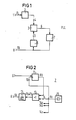
- Fig. 1 shows a phase locked loop PLL according to the prior art with an input 1 for a gap clock with the frequency FL, a frequency divider 2, a phase discriminator 3 with Inputs 4 and 5 and an output 6, a regulator and oscillator part 7, an output 8 for the clock regulated by means of the phase locked loop PLL and a frequency divider 9.
- FIG. 2 shows the regulator and oscillator part 7 in detail. This contains a summing counter 11 for averaging, a frequency divider 12, an exclusive OR gate 13 and a quartz oscillator 15.
- FIG. 3 shows a pulse plan with the auxiliary frequency FH of the output signal of the quartz oscillator 15, with the frequency FX of the output signal of the summing counter 11 and the sum of the frequencies FH + FX of both signals at the output of the exclusive OR gate 13.
- the mode of operation of the phase-locked loop according to FIGS. 1 and 2 is as follows: A gap clock with the frequency FL applied to the input 1 is divided by the frequency divider 2 in the form of a counter in such a way that a square-wave voltage at the input 4 of the phase discriminator 3 has only a fluctuating period is present. With the division factor of the frequency divider 2, a maximum possible jitter resulting, for example, from three successive gaps must be taken into account.
- the frequency divider 9 has the same structure as the frequency divider 2.
- the quartz oscillator 15 To generate the clock with the frequency FA, the quartz oscillator 15 first supplies a square-wave voltage with the auxiliary frequency FH, which is smaller than the frequency FA of the clock multiplied by the division factor N 12 of the frequency divider 12. With a permissible tolerance of the frequency of the read cycle of ⁇ AFA, FH ⁇ N 12 (FA-AFA) applies.
- FH ⁇ N 12 FH ⁇ N 12 (FA-AFA) applies.
- the frequency of the readout pulse is thus FA
- the output signal of the phase discriminator 3 controls, according to its duty cycle, via a control input which enables or blocks the clock input, the summing counter 11, whose frequency FX is equal to the mean frequency difference from FH / N 12 to FL, N 12 being the division factor of the frequency divider 12 is.
- the auxiliary frequency FH drives the exclusive OR gate 13 directly.
- the size of the summing counter 11 determines the frequency pulling range of the clock with the frequency FA and thus also the auxiliary frequency FH.
- the limit frequency FG of the jitter transfer function results from where the indices of the division factors indicate the corresponding frequency divider or the summing counter. Since there is no integrating effect in this phase locked loop, there is no jitter increase.
- a plurality of, for example, three or fifteen phase-locked loops without a crystal oscillator, each with the second input 14a, 14b ... 14n of the respective exclusive-OR gate 13, can additionally be connected to the output of the crystal oscillator 15.
- FIG. 4 shows a practical embodiment of the phase locked loop according to the invention.
- a frequency FH + FX 32.768 MHz with 0.5 UI jitter occurs at the output of the exclusive OR gate 13.
- a clock FA 2.048 MHz with a jitter (0.032 Ul) reduced by a factor of sixteen in the frequency divider 12a is output at the output 8.
Landscapes
- Engineering & Computer Science (AREA)
- Computer Networks & Wireless Communication (AREA)
- Signal Processing (AREA)
- Stabilization Of Oscillater, Synchronisation, Frequency Synthesizers (AREA)
- Networks Using Active Elements (AREA)
- Optical Communication System (AREA)
- Manipulation Of Pulses (AREA)
- Amplifiers (AREA)
Abstract
Description
- Die Erfindung bezieht sich auf einen Phasenregelkreis mit einem Phasendiskriminator, mit einem ersten Frequenzteiler, dessen Eingang als Eingang für einen Lückentakt dient und dessen Ausgang mit dem ersten Eingang des Phasendiskriminators verbunden ist, mit einem Regler-und Oszillatorteil, dessen Eingang an den Ausgang des Phasendiskriminators angeschlossen ist und dessen Ausgang der Abgabe eines geregelten Taktes dient, und mit einem zweiten Frequenzteiler, dessen Eingang mit dem Ausgang des Regler-und Oszillatorteils und dessen Ausgang mit einem zweiten Eingang des Phasendiskriminators verbunden ist.
- Ein derartiger Phasenregelkreis (phase-lockedloop) ist aus dem Buch "Halbleiter-Schaltungstechnik", Tietze/ Schenk, 6. Auflage, Springer-Verlag Berlin Heidelberg New York Tokyo, 1983, Seiten 828 und 829 bekannt.
- In der Zeitschrift "telcom report", 9 (1986) Heft 3, Seiten 190 - 197 sind weiter Digitalsignal-Multiplexgeräte beschrieben. In diesen wird in dem im Empfangsweg liegenden Demultiplexer zur Rückgewinnung des jeweiligen Unterkanals dessen Takt benötigt. Die Taktrückgewinnung erfolgt üblicherweise mit einem Phasenregelkreis PLL im Zusammenwirken mit einem Pufferspeicher. Hierbei wird der gedemultiplexte Unterkanal mit dessen Lückentakt in den Pufferspeicher eingelesen und mit dem aus diesem Lückentakt mit Hilfe eines Phasenregelkreises hoher Güte gewonnenen jitterarmen Takt ausgelesen. Phasenregelkreise hoher Güte sind wegen der Anforderung an die Jitterdämpfung notwendig.
- Der Regler-und Oszillatorteil enthält meist einen analogen Integrator, um möglichst kleine Phasenabweichungen zu erzielen. Wegen der beim Integrator vorhandenen unteren Grenzfrequenz kann es aber zu einer unerwünschten Jitterüberhöhung kommen.
- In einem Digitalsignal-Multiplexgerät DSMX 2/34 sind für die Rückgewinnung der Takte aus sechzehn 2-Mbit/s-Kanälen ebensoviele Phasenregelkreise notwendig.
- Aufgabe der Erfindung ist es, den Platz-und Kostenaufwand einer Gruppe mit mehreren Phasenregelkreisen beispielsweise in einem Digitalsignal-Multiplexgerät oder - Verteilermultiplexer zu senken.
- Ausgehend von einem Phasenregelkreis der einleitend geschilderten Art wird diese Aufgabe erfindungsgemäß dadurch gelöst, daß im Regler-und Oszillatorteil ein Summierzähler für Mittelwertbildung, dessen Steuereingang mit dem Ausgang des Phasendiskriminators verbunden ist, ein Quarzoszillator, ein Exklusiv-ODER-Gatter, dessen erster Eingang mit dem Ausgang des Summierzählers und dessen zweiter Eingang mit dem Ausgang des Quarzoszillators und dem Takteingang des Summierzählers verbunden sind, und ein dritter Frequenzteiler vorgesehen sind, dessen Eingang mit dem Ausgang des Exklusiv-ODER-Gatters verbunden ist und dessen Ausgang den Ausgang des Regler-und Oszillatorteils bildet, und daß ferner die Hilfsfrequenz des Quarzoszillators niedriger als die Frequenz des geregelten Taktes multipliziert mit dem Teilungsfaktor des dritten Frequenzteilers gewählt ist.
- Vorteilhaft ist es dabei, wenn der Ausgang des Quarzoszillators mit den zweiten Eingängen der Exklusiv-ODER-Gatter mehrerer Phasenregelkreise ohne eigenen Quarzoszillator verbunden ist.
- Damit läßt sich eine Vollintegration vieler Phasenregelkreise lediglich mit einem gemeinsamen äußeren Quarzoszillator realisieren. Bezüglich eines vorgegebenen Eigenjitters und einer nicht zulässigen Jitterüberhöhung im Jitterdämpfungsverhalten kann der dazu notwendige Schaltungsaufwand klein und der Leistungsverbrauch niedrig gehalten werden.
- Zur Regelung eines Lückentaktes einer mittleren Frequenz von 2,048 MHz ist es vorteilhaft, wenn für alle Frequenzteiler ein Teilungsfaktor 16 gewählt ist, wenn der Summierzähler bis 2048 zählt und wenn der Quarzoszillator eine Frequenz von 32,76 MHz abgibt.
- Damit ist eine vierfache Verwendung mit einem gemeinsamem Quarzoszillator in einem Digitalsignal-Multiplexgerät DSMX 2/8, eine sechzehnfache Verwendung mit einem gemeinsamem Quarzoszillator in einem Digitalsignal-Multiplexgerät DSMX 2/34 und eine mehrfache Verwendung bei anderen Digitalsignal-Multiplexern, oder - Verteilermultiplexern möglich.
- Anhand von Ausführungsbeispielen wird die Erfindung nachstehend näher erläutert.
-
- Fig. 1 zeigt einen Phasenregelkreis nach dem Stand der Technik,
- Fig. 2 zeigt einen erfindungsgemäßen Regler-und Oszillatorteil für einen Phasenregelkreis nach Figur 1,
- Fig. 3 zeigt einen Pulsplan zur Erläuterung der Wirkungsweise des Phasenregelkreises nach den Fig. 1 und 2 und
- Fig. 4 zeigt ein praktisches Ausführungsbeispiel der Erfindung.
- Fig. 1 zeigt einen Phasenregelkreis PLL nach dem Stand der Technik mit einem Eingang 1 für einen Lückentakt mit der Frequenz FL, einen Frequenzteiler 2, einen Phasendiskriminator 3 mit Eingängen 4 und 5 und einem Ausgang 6, einen Regler-und Oszillatorteil 7, einen Ausgang 8 für den mittels des Phasenregelkreises PLL geregelten Takt und einen Frequenzteiler 9.
- Fig. 2 zeigt den Regler-und Oszillatorteil 7 detailliert. Dieser enthält einen Summierzähler 11 zur Mittelwertbildung, einen Frequenzteiler 12, ein Exklusiv-ODER-Gatter 13 und einen Quarzoszillator 15.
- Figur 3 zeigt einen Pulsplan mit der Hilfsfrequenz FH des Ausgangssignals des Quarzoszillators 15, mit der Frequenz FX des Ausgangssignals des Summierzählers 11 und der Summe der Frequenzen FH + FX beider Signale am Ausgang des Exkiusiv-ODER-Gatters 13.
- Die Wirkungsweise des Phasenregelkreises nach den Figuren 1 und 2 ist wie folgt: Ein am Eingang 1 angelegter Lückentakt mit der Frequenz FL wird durch den Frequenzteiler 2 in Form eines Zählers derart geteilt, daß am Eingang 4 des Phasendiskriminators 3 eine Rechteckspannung mit lediglich noch schwankender Periodendauer anliegt. Mit dem Teilungsfaktor des Frequenzteilers 2 muß dabei ein sich beispielsweise aus drei hintereinander liegenden Lücken ergebender maximal möglicher Jitter berücksichtigt werden. Der als flankengetriggertes RS-Flipflop ausgebildete Phasendiskriminator 3 vergleicht diese Rechteckspannung mit der am Eingang 5 des Phasendiskriminators 3 anliegenden durch Teilung im Frequenzteiler 9 aus dem Takt mit der Frequenz FA abgeleiteten hinsichtlich der Phasendifferenz. Der Frequenzteiler 9 weist dafür einen gleichen Aufbau wie der Frequenzteiler 2 auf.
- Zur Erzeugung des Taktes mit der Frequenz FA liefert zuerst der Quarzoszillator 15 eine Rechteckspannung mit der Hilfsfrequenz FH, die kleiner als die Frequenz FA des Taktes multipliziert mit dem Teilungsfaktor N12 des Frequenzteilers 12 ist. Bei einer zulässigen Toleranz der Frequenz des Auslesetaktes von ± AFA gilt FH<N12 (FA-AFA). Durch regelmäßiges Umpolen während einer Halbperiode der Hilfsfrequenz FH mit der Frequenz FX über das Exkiu siv-ODER-Gatter 13 wird die mittlere Frequenz der Impulsreihe mit der Hilfsfrequenz FH auf den Wert FH+FX erhöht, wobei an den Umpoistellen jeweils ein Phasenfehler von auftritt. Dieser wird durch Teilen der lmpulsfolge mit dem Frequenzteiler 12 auf den restlichen Phasenfehler (Eigenjitter)

- Das Ausgangssignal des Phasendiskriminators 3 steuert entsprechend seinem Tastverhältnis über einen Steuereingang, der den Takteingang freigibt, bzw. sperrt, den Summierzähler 11, dessen Frequenz FX gleich dem mittleren Frequenzunterschied von FH/N12 zu FL ist, wobei N12 der Teilungsfaktor des Frequenzteilers 12 ist. Die Hilfsfrequenz FH steuert das Exklusiv-ODER-Gatter 13 direkt an. Die Größe des Summierzählers 11 bestimmt den Frequenzziehbereich des Taktes mit der Frequenz FA und damit auch die Hilfsfrequenz FH.
- Die Grenzfrequenz FG der Jitterübertragungsfunktion ergibt sich aus

- An dem Ausgang des Quarzoszillators 15 können zusätzlich mehrere beispielsweise drei oder fünfzehn Phasenregelkreise ohne Quarzoszillator jeweils mit dem zweiten Eingang 14a, 14b ... 14n des jeweiligen Exklusiv-ODER-Gatters 13 angeschlossen werden.
- Figur 4 zeigt ein praktisches Ausführungsbeispiel des erfindungsgemäßen Phasenregelkreises. Die Frequenzteiler 2a, 9a und 12a haben jeweils einen Teilungsfaktor TF=16; der Summierzähler 11 zählt bis 2048, ehe er ein Ausgangssignal abgibt. Der Quarzoszillator 15a gibt eine Hilfsfrequenz FH = 32,76 MHz ab, der Summierzähler 11 liefert im Mittel eine Frequenz FX = 0,008 MHz. Am Ausgang des Exklusiv-ODER-Gatters 13 tritt eine Frequenz FH + FX = 32,768 MHz mit 0,5 UI Jitter auf. Am Ausgang 8 wird ein Takt FA=2,048 MHz mit einem im Frequenzteiler 12a um den Faktor sechzehn reduzierten Jitter (0,032 Ul) ausgegeben.
Claims (5)
dadurch gekennzeichnet,
daß im Regler-und Oszillatorteil (7)
dadurch gekennzeichnet,
daß der Ausgang des Quarzoszillators (14) mit den zweiten Eingängen (14,14a,14b,14c) der Exklusiv-ODER-Gatter (13) mehrerer Phasenregelkreise ohne eigenen Quarzoszillator verbunden ist.
dadurch gekennzeichnet,
gekennzeichnet durch
eine vierfache Verwendung mit einem gemeinsamen Quarzoszillator (15) in einem Digitalsignal-Multiplexgerät DSMX 2/8.
gekennzeichnet durch
eine sechszehnfache Verwendung mit einem gemeinsamen Quarzoszillator, (15) in einem Digitalsignal-Multiplexgerät DSMX 2/34.
Priority Applications (1)
| Application Number | Priority Date | Filing Date | Title |
|---|---|---|---|
| AT87114958T ATE64049T1 (de) | 1986-10-20 | 1987-10-13 | Phasenregelkreis. |
Applications Claiming Priority (2)
| Application Number | Priority Date | Filing Date | Title |
|---|---|---|---|
| DE3635641 | 1986-10-20 | ||
| DE3635641 | 1986-10-20 |
Publications (2)
| Publication Number | Publication Date |
|---|---|
| EP0266588A1 true EP0266588A1 (de) | 1988-05-11 |
| EP0266588B1 EP0266588B1 (de) | 1991-05-29 |
Family
ID=6312064
Family Applications (1)
| Application Number | Title | Priority Date | Filing Date |
|---|---|---|---|
| EP87114958A Expired - Lifetime EP0266588B1 (de) | 1986-10-20 | 1987-10-13 | Phasenregelkreis |
Country Status (11)
| Country | Link |
|---|---|
| US (1) | US4820994A (de) |
| EP (1) | EP0266588B1 (de) |
| JP (1) | JPS63109609A (de) |
| AT (1) | ATE64049T1 (de) |
| AU (1) | AU579962B2 (de) |
| BR (1) | BR8705563A (de) |
| CA (1) | CA1273413A (de) |
| DE (1) | DE3770410D1 (de) |
| ES (1) | ES2022256B3 (de) |
| GR (1) | GR3002111T3 (de) |
| NO (1) | NO874371L (de) |
Cited By (3)
| Publication number | Priority date | Publication date | Assignee | Title |
|---|---|---|---|---|
| WO1989012936A1 (en) * | 1988-06-24 | 1989-12-28 | Nkt A/S | A method of adjusting the phase of a clock generator with respect to a data signal |
| EP0393341A1 (de) * | 1989-03-23 | 1990-10-24 | Siemens Aktiengesellschaft | Verfahren und Anordnung zur Umwandlung eines lückenbehafteten Einlesetaktes in einen lückenfreien Auslesetakt |
| WO1992001344A1 (en) * | 1990-07-10 | 1992-01-23 | Telefonaktiebolaget Lm Ericsson | Phase locking circuit for jitter reduction in a digital multiplex system |
Families Citing this family (1)
| Publication number | Priority date | Publication date | Assignee | Title |
|---|---|---|---|---|
| JPH0273722A (ja) * | 1988-09-09 | 1990-03-13 | Nec Corp | Pll方式オフセット周波数合成回路 |
Citations (3)
| Publication number | Priority date | Publication date | Assignee | Title |
|---|---|---|---|---|
| US3731219A (en) * | 1971-07-29 | 1973-05-01 | Int Standard Electric Corp | Phase locked loop |
| US4066978A (en) * | 1974-10-07 | 1978-01-03 | The Charles Stark Draper Laboratory, Inc. | Digital phase-locked loop filter |
| DE2925391A1 (de) * | 1979-06-21 | 1981-01-15 | Hertz Inst Heinrich | Verfahren zur uebermittlung von zeitmultiplexsignalen in einem digitalen nachrichtennetz |
Family Cites Families (5)
| Publication number | Priority date | Publication date | Assignee | Title |
|---|---|---|---|---|
| US3883817A (en) * | 1973-08-20 | 1975-05-13 | Nasa | Digital phase-locked loop |
| US4242639A (en) * | 1978-09-05 | 1980-12-30 | Ncr Corporation | Digital phase lock circuit |
| AU534342B2 (en) * | 1980-02-13 | 1984-01-19 | Motorola, Inc. | An improved frequency synthesizer using multiple dual modules prescalers |
| DE3681075D1 (de) * | 1985-06-10 | 1991-10-02 | Siemens Ag | Taktregenerator. |
| US4679004A (en) * | 1985-09-03 | 1987-07-07 | Nec Corporation | Frequency synthesizer of a phase-locked type with a sampling circuit |
-
1987
- 1987-10-07 US US07/105,670 patent/US4820994A/en not_active Expired - Fee Related
- 1987-10-13 ES ES87114958T patent/ES2022256B3/es not_active Expired - Lifetime
- 1987-10-13 DE DE8787114958T patent/DE3770410D1/de not_active Expired - Lifetime
- 1987-10-13 AT AT87114958T patent/ATE64049T1/de not_active IP Right Cessation
- 1987-10-13 EP EP87114958A patent/EP0266588B1/de not_active Expired - Lifetime
- 1987-10-16 CA CA000549458A patent/CA1273413A/en not_active Expired - Lifetime
- 1987-10-19 BR BR8705563A patent/BR8705563A/pt not_active IP Right Cessation
- 1987-10-19 JP JP62261945A patent/JPS63109609A/ja active Granted
- 1987-10-19 AU AU79906/87A patent/AU579962B2/en not_active Ceased
- 1987-10-20 NO NO874371A patent/NO874371L/no unknown
-
1991
- 1991-06-12 GR GR90401180T patent/GR3002111T3/el unknown
Patent Citations (3)
| Publication number | Priority date | Publication date | Assignee | Title |
|---|---|---|---|---|
| US3731219A (en) * | 1971-07-29 | 1973-05-01 | Int Standard Electric Corp | Phase locked loop |
| US4066978A (en) * | 1974-10-07 | 1978-01-03 | The Charles Stark Draper Laboratory, Inc. | Digital phase-locked loop filter |
| DE2925391A1 (de) * | 1979-06-21 | 1981-01-15 | Hertz Inst Heinrich | Verfahren zur uebermittlung von zeitmultiplexsignalen in einem digitalen nachrichtennetz |
Cited By (5)
| Publication number | Priority date | Publication date | Assignee | Title |
|---|---|---|---|---|
| WO1989012936A1 (en) * | 1988-06-24 | 1989-12-28 | Nkt A/S | A method of adjusting the phase of a clock generator with respect to a data signal |
| US5161173A (en) * | 1988-06-24 | 1992-11-03 | NKT A/S NKT Alle | Method of adjusting the phase of a clock generator with respect to a data signal |
| EP0393341A1 (de) * | 1989-03-23 | 1990-10-24 | Siemens Aktiengesellschaft | Verfahren und Anordnung zur Umwandlung eines lückenbehafteten Einlesetaktes in einen lückenfreien Auslesetakt |
| US5017801A (en) * | 1989-03-23 | 1991-05-21 | Siemens Aktiengesellschaft | Method and apparatus for converting a gap-infested read-in clock into a gap-free read-out clock |
| WO1992001344A1 (en) * | 1990-07-10 | 1992-01-23 | Telefonaktiebolaget Lm Ericsson | Phase locking circuit for jitter reduction in a digital multiplex system |
Also Published As
| Publication number | Publication date |
|---|---|
| US4820994A (en) | 1989-04-11 |
| ATE64049T1 (de) | 1991-06-15 |
| JPS63109609A (ja) | 1988-05-14 |
| NO874371D0 (no) | 1987-10-20 |
| NO874371L (no) | 1988-04-21 |
| CA1273413A (en) | 1990-08-28 |
| JPH0445011B2 (de) | 1992-07-23 |
| ES2022256B3 (es) | 1991-12-01 |
| DE3770410D1 (de) | 1991-07-04 |
| EP0266588B1 (de) | 1991-05-29 |
| AU7990687A (en) | 1988-04-21 |
| GR3002111T3 (en) | 1992-12-30 |
| AU579962B2 (en) | 1988-12-15 |
| BR8705563A (pt) | 1988-05-24 |
Similar Documents
| Publication | Publication Date | Title |
|---|---|---|
| DE69131066T2 (de) | Anordnung zum extrahieren von asynchronen signalen | |
| DE69027152T2 (de) | Hoch-Resolutionsabtast-Taktgenerator mit Deglitcher-Anordnung | |
| DE3308903A1 (de) | Adaptive schwellenwertvorrichtung | |
| DE2515969C3 (de) | Mehrkanalgenerator mit einer Frequenzsyntheseanordnung | |
| DE3022746A1 (de) | Digitale phasenkomparatorschaltung | |
| DE68912348T2 (de) | Verfahren zur phasenregelung eines taktgebers in bezug auf ein datensignal. | |
| DE60036445T2 (de) | Oszillator und Oszillationsverfahren | |
| EP0775400B1 (de) | Integrierbare taktgewinnungsschaltung | |
| EP0203208A1 (de) | Frequenzsyntheseschaltung zur Erzeugung eines analogen Signals mit digital in Stufen einstellbarer Frequenz | |
| DE69111669T2 (de) | Phasenkorrekturschaltung für Signale in einem System mit doppelten digitalen Leitungen. | |
| EP0903859B1 (de) | Frequenzteiler mit geringem Stromverbrauch | |
| EP0266588B1 (de) | Phasenregelkreis | |
| DE69319851T2 (de) | Diskretzeit Signalverarbeitungssystem | |
| DE102004038100B3 (de) | Erzeugung eines Takts mit gespreiztem Frequenzspektrum | |
| EP0419895A2 (de) | Taktversorgung für Multiplexsysteme | |
| DE2529448C2 (de) | Schaltungsanordnung zur Umwandlung von NRZ-Signalen in RZ-Signale, insbesondere für die synchrone Zeitmultiplexbildung | |
| DE19822777C2 (de) | Taktgenerator | |
| DE3324506C2 (de) | ||
| DE3153249C2 (en) | Phase discriminator arrangement | |
| EP0133279B1 (de) | Verfahren zur Bitraten-Transformation von Digitalsignalen | |
| DE2627830C2 (de) | System zur Verzögerung eines Signals | |
| EP0084675B1 (de) | Verfahren und Anordnung zur Taktsynchronisierung auf der Empfangsseite eines plesiochronen Übertragungssystems | |
| DE3635429A1 (de) | Phasenregelkreis | |
| DE19860964B4 (de) | Taktgenerator | |
| EP0393341A1 (de) | Verfahren und Anordnung zur Umwandlung eines lückenbehafteten Einlesetaktes in einen lückenfreien Auslesetakt |
Legal Events
| Date | Code | Title | Description |
|---|---|---|---|
| PUAI | Public reference made under article 153(3) epc to a published international application that has entered the european phase |
Free format text: ORIGINAL CODE: 0009012 |
|
| AK | Designated contracting states |
Kind code of ref document: A1 Designated state(s): AT BE CH DE ES FR GB GR IT LI NL SE |
|
| 17P | Request for examination filed |
Effective date: 19880608 |
|
| 17Q | First examination report despatched |
Effective date: 19900621 |
|
| GRAA | (expected) grant |
Free format text: ORIGINAL CODE: 0009210 |
|
| AK | Designated contracting states |
Kind code of ref document: B1 Designated state(s): AT BE CH DE ES FR GB GR IT LI NL SE |
|
| REF | Corresponds to: |
Ref document number: 64049 Country of ref document: AT Date of ref document: 19910615 Kind code of ref document: T |
|
| REF | Corresponds to: |
Ref document number: 3770410 Country of ref document: DE Date of ref document: 19910704 |
|
| ET | Fr: translation filed | ||
| ITF | It: translation for a ep patent filed | ||
| GBT | Gb: translation of ep patent filed (gb section 77(6)(a)/1977) | ||
| PLBE | No opposition filed within time limit |
Free format text: ORIGINAL CODE: 0009261 |
|
| STAA | Information on the status of an ep patent application or granted ep patent |
Free format text: STATUS: NO OPPOSITION FILED WITHIN TIME LIMIT |
|
| 26N | No opposition filed | ||
| REG | Reference to a national code |
Ref country code: GR Ref legal event code: FG4A Free format text: 3002111 |
|
| EAL | Se: european patent in force in sweden |
Ref document number: 87114958.9 |
|
| PGFP | Annual fee paid to national office [announced via postgrant information from national office to epo] |
Ref country code: GB Payment date: 19950918 Year of fee payment: 9 |
|
| PGFP | Annual fee paid to national office [announced via postgrant information from national office to epo] |
Ref country code: ES Payment date: 19950925 Year of fee payment: 9 |
|
| PGFP | Annual fee paid to national office [announced via postgrant information from national office to epo] |
Ref country code: SE Payment date: 19951019 Year of fee payment: 9 |
|
| PGFP | Annual fee paid to national office [announced via postgrant information from national office to epo] |
Ref country code: FR Payment date: 19951024 Year of fee payment: 9 |
|
| PGFP | Annual fee paid to national office [announced via postgrant information from national office to epo] |
Ref country code: CH Payment date: 19960118 Year of fee payment: 9 |
|
| PGFP | Annual fee paid to national office [announced via postgrant information from national office to epo] |
Ref country code: AT Payment date: 19961008 Year of fee payment: 10 |
|
| PG25 | Lapsed in a contracting state [announced via postgrant information from national office to epo] |
Ref country code: GB Effective date: 19961013 |
|
| PG25 | Lapsed in a contracting state [announced via postgrant information from national office to epo] |
Ref country code: SE Effective date: 19961014 Ref country code: ES Free format text: LAPSE BECAUSE OF THE APPLICANT RENOUNCES Effective date: 19961014 |
|
| PGFP | Annual fee paid to national office [announced via postgrant information from national office to epo] |
Ref country code: GR Payment date: 19961025 Year of fee payment: 10 |
|
| PG25 | Lapsed in a contracting state [announced via postgrant information from national office to epo] |
Ref country code: CH Effective date: 19961031 Ref country code: LI Effective date: 19961031 |
|
| GBPC | Gb: european patent ceased through non-payment of renewal fee |
Effective date: 19961013 |
|
| REG | Reference to a national code |
Ref country code: CH Ref legal event code: PL |
|
| PG25 | Lapsed in a contracting state [announced via postgrant information from national office to epo] |
Ref country code: FR Effective date: 19970630 |
|
| EUG | Se: european patent has lapsed |
Ref document number: 87114958.9 |
|
| REG | Reference to a national code |
Ref country code: FR Ref legal event code: ST |
|
| PG25 | Lapsed in a contracting state [announced via postgrant information from national office to epo] |
Ref country code: AT Free format text: LAPSE BECAUSE OF NON-PAYMENT OF DUE FEES Effective date: 19971013 |
|
| PG25 | Lapsed in a contracting state [announced via postgrant information from national office to epo] |
Ref country code: GR Free format text: LAPSE BECAUSE OF NON-PAYMENT OF DUE FEES Effective date: 19971031 |
|
| PGFP | Annual fee paid to national office [announced via postgrant information from national office to epo] |
Ref country code: BE Payment date: 19981016 Year of fee payment: 12 |
|
| PGFP | Annual fee paid to national office [announced via postgrant information from national office to epo] |
Ref country code: NL Payment date: 19981030 Year of fee payment: 12 |
|
| PG25 | Lapsed in a contracting state [announced via postgrant information from national office to epo] |
Ref country code: BE Free format text: LAPSE BECAUSE OF NON-PAYMENT OF DUE FEES Effective date: 19991031 |
|
| REG | Reference to a national code |
Ref country code: ES Ref legal event code: FD2A Effective date: 19991007 |
|
| PGFP | Annual fee paid to national office [announced via postgrant information from national office to epo] |
Ref country code: DE Payment date: 19991217 Year of fee payment: 13 |
|
| BERE | Be: lapsed |
Owner name: SIEMENS A.G. Effective date: 19991031 |
|
| PG25 | Lapsed in a contracting state [announced via postgrant information from national office to epo] |
Ref country code: NL Free format text: LAPSE BECAUSE OF NON-PAYMENT OF DUE FEES Effective date: 20000501 |
|
| NLV4 | Nl: lapsed or anulled due to non-payment of the annual fee |
Effective date: 20000501 |
|
| PG25 | Lapsed in a contracting state [announced via postgrant information from national office to epo] |
Ref country code: DE Free format text: LAPSE BECAUSE OF NON-PAYMENT OF DUE FEES Effective date: 20010703 |
|
| PG25 | Lapsed in a contracting state [announced via postgrant information from national office to epo] |
Ref country code: IT Free format text: LAPSE BECAUSE OF NON-PAYMENT OF DUE FEES;WARNING: LAPSES OF ITALIAN PATENTS WITH EFFECTIVE DATE BEFORE 2007 MAY HAVE OCCURRED AT ANY TIME BEFORE 2007. THE CORRECT EFFECTIVE DATE MAY BE DIFFERENT FROM THE ONE RECORDED. Effective date: 20051013 |