EP0266866A2 - Vorwärts-/Rückwärts-N-Bit-Zählregister - Google Patents
Vorwärts-/Rückwärts-N-Bit-Zählregister Download PDFInfo
- Publication number
- EP0266866A2 EP0266866A2 EP87307249A EP87307249A EP0266866A2 EP 0266866 A2 EP0266866 A2 EP 0266866A2 EP 87307249 A EP87307249 A EP 87307249A EP 87307249 A EP87307249 A EP 87307249A EP 0266866 A2 EP0266866 A2 EP 0266866A2
- Authority
- EP
- European Patent Office
- Prior art keywords
- signal
- gate
- output
- input
- counter
- Prior art date
- Legal status (The legal status is an assumption and is not a legal conclusion. Google has not performed a legal analysis and makes no representation as to the accuracy of the status listed.)
- Granted
Links
Images


Classifications
-
- H—ELECTRICITY
- H03—ELECTRONIC CIRCUITRY
- H03K—PULSE TECHNIQUE
- H03K23/00—Pulse counters comprising counting chains; Frequency dividers comprising counting chains
- H03K23/40—Gating or clocking signals applied to all stages, i.e. synchronous counters
- H03K23/50—Gating or clocking signals applied to all stages, i.e. synchronous counters using bi-stable regenerative trigger circuits
- H03K23/52—Gating or clocking signals applied to all stages, i.e. synchronous counters using bi-stable regenerative trigger circuits using field-effect transistors
Definitions
- This invention relates generally to semiconductor integrated circuit devices and more particularly, it relates to a dual mode N-bit counter which may be used to count either up or down by one or two.
- each bit cell it would therefore be desirable to provide a dual mode N-bit counter which can be used to count either up or down by one or two. It would be expedient to have such a dual mode N-bit counter contain a plurality of identical bit cells, each cell being formed with a smaller number of components than-has been traditionally required. Further, it would also be expedient to construct each bit cell to be of a regular configuration or structure so as to conform to a repeatable pattern suitable for very large scale integration (VLSI) with high packing density.
- VLSI very large scale integration
- the present invention is concerned with the provision of a counter cell for counting either up or down by one or two which includes a multiplexer section,- an increment decrement section. and a carry section.
- the multiplexer section is responsive to control counter signals and input carry signals for generating a count signal which determines the counting by one or two.
- the incrementdecrement section is responsive to the count signal and a preset input data signal for generating an incremented output signal and a decremented output signal.
- the carry section is responsive to the increment ⁇ decrement section and the input carry signals for generating a carryout-by-one signal and a carryout-by-two signal.
- three of the counter cells or stages of the present invention are arrayed to form a 3-bit counter.
- sixteen of the counter cells are arranged to form a 16-bit dual mode counter register which counts by one or two.
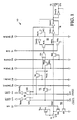
- FIG. 1 a schematic circuit diagram of a counter cell or bit 10 which is used to implement a dual mode increment / decrement N-bit counter register of the present invention.
- the counter cell 10 is constructed with a relatively small number of circuit components so as to use a reduced amount of semiconductor chip area. thereby reducing manufacturing costs and power consumption. Further, the counter cell 10 is formed as a part of a monolithic IC with a regular configuration suitable for use in large scale integration circuit arrays which may be mass produced.
- the counter cell 10 receives nine input signals consisting of a clear-counter signal CLE on input terminal 11, a load-counter signal LDCTR on input terminal 12. an increment strobe signal INCR" on input terminals l3 and 14. increment-by-one signal INCRX1 in input terminal 15. an increment-by-two signal INCRX2 on input terminal 16, an output-enable or read signal OE on input terminal 17, a preset data input or address signal D on input terminal 18, a complement carryin-by-two signal
- the counter cell provides four output signals consisting of a complement carryout-by-one signal
- COX1 on output terminal 01 a complement carryout-by-two signal COX2 on output terminal 02, an incremented output signal Q on output terminal 05, and a decremented output signal on output terminal 04.
- the counter cell 10 is formed of a multiplexer section 12, an increment/decrement section 14, a carry section 16, and an output enable or read section 18.
- the multiplexer section 12 includes a first coupling or pass N-channel MOS transistor N1 and a second coupling or pass N-channel MOS transistor N2.
- the transistor N1 has its drain connected to the input terminal 110 for receiving the complement carryin-by-one signal CINX1.
- the transistor N2 has its drain connected to the input terminal 19 for receiving the complement carryin-by-two signal CINX2.
- the terminals 19 and 110 are connected to a ground potential since this bit is always changed.
- the sources of the transistors N1 and N2 are connected together and to an internal node A for providing a count signal.
- the gate of the transistor N1 is connected to the input terminal 15 for receiving the increment-by-one or count-by-one signal INCRX1-
- This signal INCRX 1 is a control signal which is used to cause the cell to count by one.
- the gate of the transistor N2 is connected to the input terminal 16 for receiving the increment-by-two or count-by-two signal INCRX2.
- This signal INCRX2 is a control signal which is used to cause the cell to count by two.
- the increment/decrement section 14 includes a two-input NOR logic gate G1, pass N-channel MOS transistors N3-N7, and inverters INV1-INV4.
- the NOR gate G1 has one of its inputs connected to the input terminal 14 for receiving the increment strobe signal INCR * and has its other input connected to the source of the transistor N3.
- the transistor N3 has its drain connected to the count signal at the internal node A defining the output of the multiplexer section 12.
- the output of the NOR gate G1 is connected to the gate of the transistor N4.
- the transistor N4 has its drain connected to the output of the fourth inverter INV4.
- the transistor N4 has its source connected to the source of the transistor N5, the drain of the transistor N6, and to the input of the first inverter INV1.
- the transistor N5 has its drain connected to the input terminal 18 for receiving the preset data input signal D and its gate connected to the input terminal 12 for receiving the load-counter signal LDCTR.
- the transistor N6 has its gate connected to the input terminal 11 for receiving the clear-counter signal CLR and its source connected to a ground potential.
- the first and second inverters INV1, INV2 define a latch in which the output of the first inverter INV1 is connected to the input of the second inverter INV2 and the output of the second inverter INV2 is connected to the input of the first inverter INV1 via a resistor R.
- the resistor R may be implemented by an N-channel depletion-mode MOS transistor whose gate and drain electrodes are connected together as is well known in the art.
- the output of the second inverter INV2 is connected to the output terminal 05 which provides the incremented output signal Q. Further, the output of the second inverter INV2 is connected to the input of the third inverter INV3.
- the output of the third inverter INV3 is connected to the output terminal 04 which provides the decremented signal Q.
- the output of the second inverter INV2 is also connected to the drain of the transistor N7 whose source is joined to the input of the fourth inverter INV4.
- the gate of the transistor N7 is connected to the input terminal 13 for receiving the increment strobe signal INCR*.
- the carry section 16 includes a pair of two-input NOR logic gates G2, G3 and a pair of fifth and sixth inverters INV5, INV6.
- the NOR gate G2 has one of its inputs connected to one input of the NOR gate G3 and to the output of the first inverter INV1.
- the other input of the NOR gate G2 is connected to the input terminal 110 for receiving the complement carryin-by-one signal CINX1.
- the other input of the NOR gate G3 is connected to the input terminal 19 for receiving the complement carryin-by-two signal CINX2.
- the output of the NOR gate G2 is connected to the input of the fifth inverter INV5 whose output is connected to the output terminal 01 for supplying the complement carryout-by-one signal COX1.
- the output of the NOR gate G3 is connected to the input of the sixth inverter INV6 whose output is connected to the output terminal 02 for supplying the complement carryout-by-two signal COX2.
- the read section 18 includes a depletion mode transistor DM, an eight pass N-channel MOS transistor N8, and a ninth pass N-channel MOS transistor N9.
- the transistor DM has its gate and source electrodes connected together and to the input terminal 18.
- the transistor DM has its drain connected to a supply potential or voltage VCC.
- the common gate and source electrodes of the transistor DM is further joined to the drain of the eighth transistor N8.
- the eighth pass transistor N8 has its gate connected to the input terminal 17 for receiving the output-enable signal OE and has its source connected to the drain of the ninth pass transistor N9.
- the ninth pass transistor N9 has its gate connected to the output of the third inverter INV3 and its source connected to the ground potential.
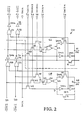
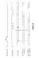
- FIGs 5(a) through 5(e) are timing diagrams which are useful in understanding the operation of the counter cell 10.
- the load-counter signal LDCTR is used to load or preset the data value into the counter cell at a time interval t1 as is shown in Figure 5(a).
- the increment strobe signal INCR* is at a high or "1" logic level as is illustrated in Figure 5(b).
- the current data value AO shown in Figure 5(c) is loaded into the counter cell during this time interval t1.
- the increment strobe signal INCR' of Figure 5(b) is pulled to a low or "0" logic level.
- the counter cell counts by one or two dependent upon which one of the control signals INCRX1 or INCRX2 illustrated in Figure 5(d) is high. It will be noted that the control signal INCRX1 or INCRX2 must be valid prior to the time when the increment strobe signal INCR' goes low and must remain valid during the time interval t2.
- control signal INCX1 applied to the input terminal 15 is at a high logic level, then the counter cell will count by one. If the control signal INCX2 applied to the input terminal 16 is at a high logic level, then the counter cell will count by two. It should be understood that only one of the input terminals 15 or 16 will be at a "1" logic level.
- the complement carryout-by-one signal COX1 from the counter cell is fed to the input terminal 110 of the next higher bit cell.
- carryout-by-two signal COX2 from the counter cell is fed to the input terminal 19 of the next higher bit cell.
- the carryin signals CINX1 and CINX2 affect whether the next preceding bit cell will count or not count and are illustrated in Figure 5(e).
- the values of the carryin signals CINX1 and CINX2 depend upon the data value AO loaded during the time interval t1, or changed value of A0 from previous t2. It will be noted that the carryin signals must be valid prior to the time interval t2 when the increment strobe signal INCR* goes low.
- any number of identical counter cells or bits 10 referred to as a counter stage can be arrayed to implement a dual mode N-bit counter of the present invention which can be used to count either up or down by one or two.
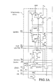
- the counter 210 is formed of two identical cells CO and C1. Each of the cells CO and C1 is similar to the cell 10 of Figure 1, with the like parts being designated by the same reference numerals. It will be noted that a third inverter INV3 of Figure 1 has been omitted since this circuit functions as an up/counter counting either by one or two.
- FIG. 3 there is illustrated a three-bit up/down counter 310 which counts by one.
- the counter 310 is formed of three identical cells C0, C1 and C2.
- Each of the cells C0, C1, C2 is similar to the cell 10 of Figure 1, with like parts being designated by the same reference numerals.
- the third inverter INV3 of Figure 1 has been replaced by a buffer section 20 which provides the incremented output signals A0, A1, A2 and the decremented output signals AO*, A1*, A2*.
- the buffer section 20 has been added to enable a higher drive capability.
- the logic gate G3 and the inverter INV6 have been omitted since this circuit functions as an up/down counter which counts by one.
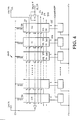
- FIG 4 there is illustrated in block diagram form a 16-bit up / down counter 410 for counting by one or two which represents a preferred embodiment of the present invention.
- the counter 410 is formed of sixteen identical cells or stages C0, C1...C15. Each of the cells C0, C1...C15 is similar to the cell 10 of Figure 1.
- the preset data input signals ADOO...AD15 are fed to corresponding ones of the cells C0...C15 via the input terminals I8.
- Each cell further receives the output-enable or read signal OE on its input terminal 17, the load-counter signal LDCTR on its input terminal 12, the increment strobe signal INCR' on its input terminals 13 and 14, the complement carryin-by-one signal CINX1 on its input terminal 19, and the complement carryin-by-two signal CINX2 on the input terminal 110.
- Each cell provides the incremented output signal on the output terminal 05 and the decremented output signal on the output terminal 04.
- the complement carryout-by-one signal COX1 is provided on the output terminal 01.
- the complement carryout-by-two signal COX2 is provided on the output terminal 02. Except for the bit "0”, each cell has its input terminals I9 and 110 connected to the respective output terminals 02 and 01 of the next lower cell. For the bit "0", the input terminals 19 an 110 are connected to a ground potential since this cell is always changed.
- the present invention provides an improved counter cell for counting either up or down by one or two which includes a multiplexer section, an increment/decrement section, and a carry section. Further. any number of such counter cells may be connected to form an N-bit counter which counts either up or down by one or two.
Landscapes
- Logic Circuits (AREA)
- Communication Control (AREA)
- Data Exchanges In Wide-Area Networks (AREA)
- Synchronisation In Digital Transmission Systems (AREA)
- Time-Division Multiplex Systems (AREA)
- Stabilization Of Oscillater, Synchronisation, Frequency Synthesizers (AREA)
- Electronic Switches (AREA)
- Analysing Materials By The Use Of Radiation (AREA)
Priority Applications (1)
| Application Number | Priority Date | Filing Date | Title |
|---|---|---|---|
| AT87307249T ATE87154T1 (de) | 1986-11-05 | 1987-08-17 | Vorwaerts-/rueckwaerts-n-bit-zaehlregister. |
Applications Claiming Priority (2)
| Application Number | Priority Date | Filing Date | Title |
|---|---|---|---|
| US06/927,308 US4706266A (en) | 1986-11-05 | 1986-11-05 | Dual mode-increment/decrement N-bit counter register |
| US927308 | 1986-11-05 |
Publications (3)
| Publication Number | Publication Date |
|---|---|
| EP0266866A2 true EP0266866A2 (de) | 1988-05-11 |
| EP0266866A3 EP0266866A3 (en) | 1990-05-02 |
| EP0266866B1 EP0266866B1 (de) | 1993-03-17 |
Family
ID=25454547
Family Applications (1)
| Application Number | Title | Priority Date | Filing Date |
|---|---|---|---|
| EP87307249A Expired - Lifetime EP0266866B1 (de) | 1986-11-05 | 1987-08-17 | Vorwärts-/Rückwärts-N-Bit-Zählregister |
Country Status (5)
| Country | Link |
|---|---|
| US (1) | US4706266A (de) |
| EP (1) | EP0266866B1 (de) |
| JP (1) | JP2719620B2 (de) |
| AT (1) | ATE87154T1 (de) |
| DE (1) | DE3784838T2 (de) |
Cited By (1)
| Publication number | Priority date | Publication date | Assignee | Title |
|---|---|---|---|---|
| WO1996037824A1 (en) * | 1995-05-26 | 1996-11-28 | National Semiconductor Corporation | Incrementor/decrementor |
Families Citing this family (7)
| Publication number | Priority date | Publication date | Assignee | Title |
|---|---|---|---|---|
| US5159696A (en) * | 1990-07-27 | 1992-10-27 | Microelectronics And Computer Technology Corporation | Maskable cascade counter |
| US6947077B1 (en) * | 1998-03-30 | 2005-09-20 | Micron Technology, Inc. | Fast and accurate adjustment of gain and exposure time for image sensors |
| US6668298B1 (en) * | 1999-12-29 | 2003-12-23 | Intel Corporation | Shifting an input signal from a high-speed domain to a lower-speed domain |
| US7899190B2 (en) | 2004-04-16 | 2011-03-01 | Research In Motion Limited | Security countermeasures for power analysis attacks |
| US7848514B2 (en) | 2004-05-24 | 2010-12-07 | Research In Motion Limited | Table masking for resistance to power analysis attacks |
| DE602005002349T2 (de) * | 2005-05-10 | 2008-01-17 | Research In Motion Ltd., Waterloo | Schlüsselmaskierung für kryptographische Prozesse |
| WO2014028005A1 (en) * | 2012-08-14 | 2014-02-20 | Empire Technology Development Llc | Software-based side-channel attack prevention |
Family Cites Families (5)
| Publication number | Priority date | Publication date | Assignee | Title |
|---|---|---|---|---|
| US3546597A (en) * | 1968-03-28 | 1970-12-08 | Collins Radio Co | Frequency divider circuit |
| US4280190A (en) * | 1979-08-09 | 1981-07-21 | Motorola, Inc. | Incrementer/decrementer circuit |
| US4509183A (en) * | 1982-09-16 | 1985-04-02 | Helene R. Wright | Bidirectional transition counter with threshold output |
| US4611337A (en) * | 1983-08-29 | 1986-09-09 | General Electric Company | Minimal logic synchronous up/down counter implementations for CMOS |
| JP5636826B2 (ja) | 2010-08-31 | 2014-12-10 | 株式会社リコー | スイッチングレギュレータ |
-
1986
- 1986-11-05 US US06/927,308 patent/US4706266A/en not_active Expired - Lifetime
-
1987
- 1987-08-17 AT AT87307249T patent/ATE87154T1/de not_active IP Right Cessation
- 1987-08-17 DE DE8787307249T patent/DE3784838T2/de not_active Expired - Fee Related
- 1987-08-17 EP EP87307249A patent/EP0266866B1/de not_active Expired - Lifetime
- 1987-08-31 JP JP62219015A patent/JP2719620B2/ja not_active Expired - Fee Related
Cited By (1)
| Publication number | Priority date | Publication date | Assignee | Title |
|---|---|---|---|---|
| WO1996037824A1 (en) * | 1995-05-26 | 1996-11-28 | National Semiconductor Corporation | Incrementor/decrementor |
Also Published As
| Publication number | Publication date |
|---|---|
| EP0266866B1 (de) | 1993-03-17 |
| DE3784838D1 (de) | 1993-04-22 |
| EP0266866A3 (en) | 1990-05-02 |
| DE3784838T2 (de) | 1993-08-19 |
| US4706266A (en) | 1987-11-10 |
| ATE87154T1 (de) | 1993-04-15 |
| JPS63125019A (ja) | 1988-05-28 |
| JP2719620B2 (ja) | 1998-02-25 |
Similar Documents
| Publication | Publication Date | Title |
|---|---|---|
| US4692634A (en) | Selectable multi-input CMOS data register | |
| US4706266A (en) | Dual mode-increment/decrement N-bit counter register | |
| US5027012A (en) | Programmable logic circuit using wired-or tristate gates | |
| EP0187698A2 (de) | Symmetrische Volladdiererschaltung | |
| JPS59114924A (ja) | Plaカウンタ | |
| EP0202910A2 (de) | Dekodierschaltung für eine Halbleiterspeicheranordnung | |
| US7480165B1 (en) | Microcontroller with programmable logic | |
| US4395646A (en) | Logic performing cell for use in array structures | |
| US5175753A (en) | Counter cell including a latch circuit, control circuit and a pull-up circuit | |
| US4686691A (en) | Multi-purpose register for data and control paths having different path widths | |
| US4513432A (en) | Multiple self-contained logic gate counter circuit | |
| US4631425A (en) | Logic gate circuit having P- and N- channel transistors coupled in parallel | |
| US5309043A (en) | Compound logic circuit having NAND and NOR gate outputs and two transistors connected within both gate circuits | |
| US4918657A (en) | Semiconductor memory device provided with an improved precharge and enable control circuit | |
| EP0228649A2 (de) | CMOS-Enkoderschaltung | |
| US4891534A (en) | Circuit for comparing magnitudes of binary signals | |
| US4924440A (en) | MOS gate array devices | |
| EP0168230B1 (de) | Multiplexier-Dekodier-Schaltungseinheit | |
| JP3200132B2 (ja) | マルチプレクサ回路 | |
| EP0250174B1 (de) | Inkrementierer und Dekrementierer | |
| US5039885A (en) | Single function programmable logic array circuit | |
| EP0308591A2 (de) | Programmierbare Logikanordnungen | |
| US7307295B2 (en) | Method and an apparatus for a hard-coded bit value changeable in any layer of metal | |
| US5446401A (en) | Synchronous dual word decoding using PLA | |
| JPH0834427B2 (ja) | 論理回路 |
Legal Events
| Date | Code | Title | Description |
|---|---|---|---|
| PUAI | Public reference made under article 153(3) epc to a published international application that has entered the european phase |
Free format text: ORIGINAL CODE: 0009012 |
|
| AK | Designated contracting states |
Kind code of ref document: A2 Designated state(s): AT BE CH DE ES FR GB GR IT LI LU NL SE |
|
| PUAL | Search report despatched |
Free format text: ORIGINAL CODE: 0009013 |
|
| AK | Designated contracting states |
Kind code of ref document: A3 Designated state(s): AT BE CH DE ES FR GB GR IT LI LU NL SE |
|
| 17P | Request for examination filed |
Effective date: 19900806 |
|
| 17Q | First examination report despatched |
Effective date: 19910828 |
|
| GRAA | (expected) grant |
Free format text: ORIGINAL CODE: 0009210 |
|
| AK | Designated contracting states |
Kind code of ref document: B1 Designated state(s): AT BE CH DE ES FR GB GR IT LI LU NL SE |
|
| PG25 | Lapsed in a contracting state [announced via postgrant information from national office to epo] |
Ref country code: IT Free format text: LAPSE BECAUSE OF FAILURE TO SUBMIT A TRANSLATION OF THE DESCRIPTION OR TO PAY THE FEE WITHIN THE PRE;WARNING: LAPSES OF ITALIAN PATENTS WITH EFFECTIVE DATE BEFORE 2007 MAY HAVE OCCURRED AT ANY TIME BEFORE 2007. THE CORRECT EFFECTIVE DATE MAY BE DIFFERENT FROM THE ONE RECORDED.SCRIBED TIME-LIMIT Effective date: 19930317 Ref country code: BE Effective date: 19930317 Ref country code: GR Free format text: LAPSE BECAUSE OF FAILURE TO SUBMIT A TRANSLATION OF THE DESCRIPTION OR TO PAY THE FEE WITHIN THE PRESCRIBED TIME-LIMIT Effective date: 19930317 Ref country code: LI Effective date: 19930317 Ref country code: CH Effective date: 19930317 Ref country code: SE Effective date: 19930317 Ref country code: FR Effective date: 19930317 Ref country code: AT Effective date: 19930317 |
|
| REF | Corresponds to: |
Ref document number: 87154 Country of ref document: AT Date of ref document: 19930415 Kind code of ref document: T |
|
| REF | Corresponds to: |
Ref document number: 3784838 Country of ref document: DE Date of ref document: 19930422 |
|
| PG25 | Lapsed in a contracting state [announced via postgrant information from national office to epo] |
Ref country code: ES Free format text: LAPSE BECAUSE OF FAILURE TO SUBMIT A TRANSLATION OF THE DESCRIPTION OR TO PAY THE FEE WITHIN THE PRESCRIBED TIME-LIMIT Effective date: 19930628 |
|
| REG | Reference to a national code |
Ref country code: CH Ref legal event code: PL |
|
| EN | Fr: translation not filed | ||
| PG25 | Lapsed in a contracting state [announced via postgrant information from national office to epo] |
Ref country code: LU Free format text: LAPSE BECAUSE OF NON-PAYMENT OF DUE FEES Effective date: 19930831 |
|
| PLBE | No opposition filed within time limit |
Free format text: ORIGINAL CODE: 0009261 |
|
| STAA | Information on the status of an ep patent application or granted ep patent |
Free format text: STATUS: NO OPPOSITION FILED WITHIN TIME LIMIT |
|
| 26N | No opposition filed | ||
| REG | Reference to a national code |
Ref country code: GB Ref legal event code: IF02 |
|
| PGFP | Annual fee paid to national office [announced via postgrant information from national office to epo] |
Ref country code: NL Payment date: 20020618 Year of fee payment: 16 |
|
| PGFP | Annual fee paid to national office [announced via postgrant information from national office to epo] |
Ref country code: GB Payment date: 20020626 Year of fee payment: 16 |
|
| PGFP | Annual fee paid to national office [announced via postgrant information from national office to epo] |
Ref country code: DE Payment date: 20020830 Year of fee payment: 16 |
|
| PG25 | Lapsed in a contracting state [announced via postgrant information from national office to epo] |
Ref country code: GB Free format text: LAPSE BECAUSE OF NON-PAYMENT OF DUE FEES Effective date: 20030817 |
|
| PG25 | Lapsed in a contracting state [announced via postgrant information from national office to epo] |
Ref country code: NL Free format text: LAPSE BECAUSE OF NON-PAYMENT OF DUE FEES Effective date: 20040301 |
|
| PG25 | Lapsed in a contracting state [announced via postgrant information from national office to epo] |
Ref country code: DE Free format text: LAPSE BECAUSE OF NON-PAYMENT OF DUE FEES Effective date: 20040302 |
|
| GBPC | Gb: european patent ceased through non-payment of renewal fee |
Effective date: 20030817 |
|
| NLV4 | Nl: lapsed or anulled due to non-payment of the annual fee |
Effective date: 20040301 |