EP0266997A2 - Horizontal-Ablenkschaltung mit Rasterkorrektur - Google Patents
Horizontal-Ablenkschaltung mit Rasterkorrektur Download PDFInfo
- Publication number
- EP0266997A2 EP0266997A2 EP87309697A EP87309697A EP0266997A2 EP 0266997 A2 EP0266997 A2 EP 0266997A2 EP 87309697 A EP87309697 A EP 87309697A EP 87309697 A EP87309697 A EP 87309697A EP 0266997 A2 EP0266997 A2 EP 0266997A2
- Authority
- EP
- European Patent Office
- Prior art keywords
- trace
- capacitance
- current
- retrace
- voltage
- Prior art date
- Legal status (The legal status is an assumption and is not a legal conclusion. Google has not performed a legal analysis and makes no representation as to the accuracy of the status listed.)
- Granted
Links
Images


Classifications
-
- H—ELECTRICITY
- H04—ELECTRIC COMMUNICATION TECHNIQUE
- H04N—PICTORIAL COMMUNICATION, e.g. TELEVISION
- H04N3/00—Scanning details of television systems; Combination thereof with generation of supply voltages
- H04N3/10—Scanning details of television systems; Combination thereof with generation of supply voltages by means not exclusively optical-mechanical
- H04N3/16—Scanning details of television systems; Combination thereof with generation of supply voltages by means not exclusively optical-mechanical by deflecting electron beam in cathode-ray tube, e.g. scanning corrections
- H04N3/22—Circuits for controlling dimensions, shape or centering of picture on screen
- H04N3/23—Distortion correction, e.g. for pincushion distortion correction, S-correction
-
- H—ELECTRICITY
- H04—ELECTRIC COMMUNICATION TECHNIQUE
- H04N—PICTORIAL COMMUNICATION, e.g. TELEVISION
- H04N3/00—Scanning details of television systems; Combination thereof with generation of supply voltages
- H04N3/10—Scanning details of television systems; Combination thereof with generation of supply voltages by means not exclusively optical-mechanical
- H04N3/16—Scanning details of television systems; Combination thereof with generation of supply voltages by means not exclusively optical-mechanical by deflecting electron beam in cathode-ray tube, e.g. scanning corrections
- H04N3/22—Circuits for controlling dimensions, shape or centering of picture on screen
- H04N3/23—Distortion correction, e.g. for pincushion distortion correction, S-correction
- H04N3/233—Distortion correction, e.g. for pincushion distortion correction, S-correction using active elements
Definitions
- This invention relates to a deflection circuit in which a supply current is coupled to a trace capacitor of the deflection circuit through a plurality of current paths.
- a retrace capacitance is coupled across the deflection winding during the retrace interval to form a retrace resonant circuit. Energy is replenished during retrace via a flyback transformer.
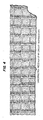
- each vertical strip of the crosshatch pattern may appear as being of a zig-zag shape, instead of a straight line shape.
- the zig-zag shape appears in a given vertical strip immediately below the intersection point with a horizontal strip.
- Such distortions are sometimes referred to by the name "mouseteeth" distortions.
- “Mouseteeth” distortions may be reduced using an arrangement such as described in UK Published application 2150796A, published 3 July 1985, corresponding to U.S. Patent No. 4,634,937, entitled EAST-WEST CORRECTION CIRCUIT, issued to P.E. Haferl on 6 January 1987, that is referred to herein as the Haferl patent, by supplying an E-W modulation current generated by an east-west control circuit via a choke having a high impedance. This choke integrates the horizontal frequency components resulting in a sink current that is substantially a D.C. current that flows from the deflection circuit to the E-W control circuit.
- Deflection disturbances referred to as “mouseteeth” are avoided because of the loose coupling between the flyback transformer and the deflection winding during the retrace interval.
- the loose coupling is provided by the choke that provides high frequency isolation of the deflection circuit output stage from the E-W control circuit.
- Color television picture tubes with a large faceplate radius R such as, for example, Philips 45AX picture tube, may require a significantly high amount of inside pincushion correction.
- a deflection apparatus includes a deflection winding for generating scanning current at a deflection rate.
- a trace capacitance is coupled to the deflection winding.
- a supply inductance is coupled to the trace capacitance to provide a first current path for conducting a first portion of a supply current.
- a circuit branch, including a second capacitance and a second inductance, that is coupled to the trace capacitance forms with the trace capacitance a second resonant circuit for generating in the second inductance a second current.
- the second current is coupled to the trace capacitance to vary a parabolic voltage in the trace capacitance in accordance with the amplitude of the second current in a manner to reduce, for example, inside pincushion distortion.
- a voltage in the second capacitance is combined at a terminal of the second inductance with the parabolic voltage in the trace capacitance to reduce an alternating current voltage at the terminal.
- a second portion of the supply current is coupled to the trace capacitance through the terminal to reduce a discharge current from the trace capacitor during retrace.
- mouseteeth distortions are also reduced.
- a scanning current is generated in a deflection winding at a deflection rate during trace and retrace intervals of a deflection cycle.
- the deflection winding is included in a retrace resonant circuit during the retrace interval.
- Switching means that is coupled to the deflection winding, responsive to an input signal at a first frequency that is related to the deflection rate, generates, during the retrace interval, a retrace voltage.
- a trace capacitance coupled to the deflection winding forms with the deflection winding a first trace resonant circuit during the trace interval such that the scanning current in the trace capacitance develops a parabolic voltage in the trace capacitance during the trace interval.
- a supply voltage is developed at a supply terminal.
- a supply inductance is coupled between the supply voltage and the trace capacitance for supplying via the supply inductance a first portion of a DC supply current that replenishes a first portion of energy losses in the retrace resonant circuit.
- a second portion of the DC supply current is coupled to the trace capacitance in a current path that bypasses the supply inductance for replenishing a second portion of the energy losses.
- a deflection circuit 100 of FIGURE 1, embodying an aspect of the invention, may provide horizontal deflection of the electron beams in, for example, a Philips 110° 45AX FS color picture tube type A66-EAK00X01.
- a source of regulated direct current voltage B+ developed between a terminal 22 and ground, is coupled through a small-valued resistor R1 to a terminal 22a of a primary winding W1 of a horizontal flyback transformer T1.
- the other terminal of winding W1 is coupled to a junction terminal 23.
- a filtering capacitance C1 is coupled from terminal 22a to ground.
- Regulated voltage B+ is generated, for example, by a switched mode power supply 90.
- a secondary winding W3 of transformer T1 supplies an ultor voltage U through a rectifying diode D40.
- a horizontal output transistor Q1 operating at a deflection rate f H and having its base coupled to a conventional driver and oscillator circuit 50, has its collector-to-emitter path coupled between junction terminal 23 and ground. Circuit 50 is synchronized by a sync signal H s and by a retrace pulse representative signal H r , in a well known manner.
- Paralleling transistor Q1 is the series arrangement of two rectifiers, diodes D1 and D2 operating as a damper diode arrangement. Coupled in parallel with the anode and cathode electrodes of diode D1 is an arrangement of a horizontal deflection winding L H that is coupled to an S-shaping, or trace, capacitance C s .
- a deflection retrace capacitance C RD coupled also across the anode and cathode electrodes of diode D1, forms with deflection winding L H , a parallel retrace resonant circuit 27.
- a second retrace capacitance C RT is coupled between a junction terminal 28 and ground.
- a small-valued capacitance C P is coupled between terminal 23 and ground.
- Capacitance C P provides fine tuning of the resonance frequency of retrace resonance circuit 27. Coupled between terminal 28 and ground is a series arrangement of a diode D3 and a controllable East-West current source 25 that includes a current sink transistor Q4 having, at the collector electrode, a high output impedance during retrace.
- the collector electrode of transistor Q4 is coupled via a diode D3 to terminal 28 to provide a modulated sink current i3 that varies in a vertical rate parabolic manner.
- Diode D3 decouples the collector of transistor Q4 from ground, toward the end of trace, when diode D2 conducts, to prevent the flow of saturation collector current in transistor Q4, prior to retrace.
- An inside pincushion distortion correction circuit 60 includes an inductance L1 that is coupled to a terminal 60a at the junction of capacitance C s and inductor L H .
- a capacitor C6 of circuit 60 is coupled between a terminal 60b of inductance L1 and ground.
- deflection current i1 flows, in a direction opposing the arrow, in deflection winding L H and in diode D1.
- deflection current i1 flows in deflection winding L H , in the direction of the arrow, and in diode D2 and transistor Q1 that is conductive.
- transistor Q1 becomes nonconductive and a retrace voltage V1 is developed between terminal 23 and ground.
- the high output impedance of transistor Q4 that is interposed between winding W1 and retrace resonant circuit 27 prevents, during horizontal retrace, an undesirable high frequency coupling through current source 25 between winding W1 of flyback transformer T1 and retrace resonant circuit 27 that, otherwise, could have caused "mouseteeth" distortion.
- “Mouseteeth” distortion can also be reduced by supplying East-West modulated current, instead of through the high output impedance of the transistor, via a choke having a high impedance.
- the choke may be expensive. An example of such arrangement is described in the Haferl patent that was mentioned before.
- Capacitor C RT is coupled to winding W1 via ground and capacitor C1 to form a second retrace resonant circuit that is coupled to retrace resonant circuit 27 so as to form a combined retrace resonant circuit that includes winding W1, capacitor C RT and retrace resonant circuit 27.
- the combined retrace resonant circuit is tuned to, for example, the retrace frequency.
- each of retrace resonant circuit 27 and the second retrace resonant circuit that includes winding W1 and capacitor C RT is tuned to a frequency that may be lower than the retrace frequency.
- Capacitor C RT causes the retrace voltage across winding W1 and that across deflection winding L H to occur simultaneously. Therefore, retrace voltage H r across winding W4 that provides synchronization information to Driver and oscillator 50, advantageously, contains the same synchronization information as of the retrace voltage across deflection winding L H or as of voltage V41 across capacitor C RD .
- the purpose of capacitor C RT is described in detail in the Haferl patent.
- Capacitor C RT determines the lowest deflection current amplitude that corresponds with current i3 that is zero.
- transistor Q4 of E-W control circuit 25 of FIGURE 1 operates, during the rest of horizontal retrace interval, as a Class A sink current amplifier.
- Sink current i3 in transistor Q4 develops a proportional feedback voltage V R4 across a resistor R4 that is coupled between the emitter of transistor Q4 and ground.
- Voltage V R4 is fed back to the base of a transistor Q3 via a resistor R5.
- the collector of transistor Q3 is coupled to the base of transistor Q4 at a terminal 25a.
- the amplitude of sink current i3, during retrace is kept independent from variations of the shape and amplitude of voltage V3, for example, by the negative feedback arrangement of resistors R4 and R5; therefore, high output impedance at the retrace frequency and above is established at the collector of transistor Q4.
- the average amplitude of sink current i3 is adjusted by a width control resistor R11, which determines, the emitter voltage of transistor Q3, in accordance with a vertical parabola voltage V10, that is described below.
- the average value of current i3 is modulated at a vertical rate in a parabolic manner in accordance with voltage V10.
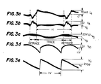
- FIGURES 2a-2f and 3a-3e illustrate wavefroms useful in explaining the operation of the arrangement of FIGURE 1. Similar numbers and symbols in FIGURES 1, 2a-2f and 3a-3e indicate similar items or functions.
- Parabola voltage V10 of FIGURE 1 is generated across a capacitor C c of, for example, a conventional vertical deflection circuit 300.
- Parabola voltage V10 of FIGURE 3d is AC coupled to the emitter of transistor Q3 of FIGURE 1 via a DC blocking capacitor C4, a resistor R14 and an adjustable E-W control resistor R12.
- Retrace voltage V3 is coupled via a diode D3, a time-integrating network, or lowpass filter that includes a resistor R2 and a capacitor C2 that filters out frequencies above the vertical frequency.
- the lowpass filtered voltage is coupled, via a resistor R3, to the emitter of transistor Q3.
- the low frequency negative feedback voltage that develops across capacitor C2 causes the average value of voltage V3 to vary in a vertical rate parabolic manner in accordance with vertical parabola voltage V10. Because of the negative feedback, the peak, for example, of the vertical rate envelope of voltage V3 is inversely related to the vertical parabola voltage applied across emitter-base junction of transistor Q3 that is obtained from voltage V10.
- Such low frequency feedback arrangement of resistors R2 and R3 provides DC stabilization and improves linearly.
- a vertical sawtooth voltage V11 that provides trapeze correction, shown in FIGURE 3e, that is obtained across a resistor R s of FIGURE 1.
- Resistor R s is coupled in series with a vertical deflection winding L v and capacitor C c of circuit 300.
- Correction of inside pincushion distortion is accomplished by the "S"-shaping of deflection current i1, in accordance with an inside pincushion correction modulation current i2 that flows in capacitance C6 an in inductor L1 of inside pincushion distortion correction circuit 60.
- Current i2 that flows in a current path that includes trace capacitance C2, varies a voltage V cs across trace capacitance C s , during trace, at a frequency that is higher than the trace resonance frequency of the trace resonant circuit that includes deflection winding L H and trace capacitance C s .
- the amplitude of current i2 is modulated by voltage V3 of FIGURE 2f at terminal 28 of FIGURE 1 to provide inside pincushion correction.
- circuit 60 is described in more detail in European Published Patent Application No. 0236064 entitled PINCUSHION CORRECTION IN DEFLECTION CIRCUIT, in the name of RCA Corporation, published 9 September 1987.
- Capacitance C6 and inductor L1 of circuit 60 form, with trace capacitance C s and deflection winding L H , a resonance circuit portion of correction circuit 60 during trace.
- the resonance circuit portion of circuit 60 is tuned by inductor L1 to a frequency that is lower than frequency f H so that current i2 will not reach zero value prior to the end of horizontal trace; yet, it is tuned to a frequency that is substantially higher than the resonance frequency of the trace resonant circuit of deflection winding L H and trace capacitance C s .
- Inside pin modulation inductor L1 may be of a variable type if an adjustable amount of correction is required. For the circuit values showing in FIGURE 1, inductor L1 may tune the resonance circuit portion of circuit 60 to a frequency of, for example, 14 KHz.
- the portion of voltage V cs that is caused by deflection current i1 is generally a parabola shaped waveform that, in each horizontal period H, is composed of trace and retrace sinewave portions, respectively.
- the corresponding sinewave portion of voltage V cs is at a frequency that is approximately equal to the trace resonance frequency of winding L H and capacitor C s .
- Such resonance frequency is for example, equal to approximately 7 KHz.
- the corresponding sinewave portion is at approximately 44 KHz.
- Inductor L1 and capacitance C6 are included in a circuit branch that, during trace, is coupled in parallel with trace capacitance C s .
- resonance current i2 flows, in a direction opposite to the arrow, from ground, through capacitance C6, inductor L1, capacitance C s , diode D1, deflection transistor Q1 that is conductive and back to ground.
- current i2 circulates in the direction of the arrow, from ground, through diode, D2, capacitance C s , inductor L1 and capacitance C6 and back to ground.
- Deflection current i1 flows, during retrace, in a current path that includes retrace capacitor C RD , deflection winding L H and trace capacitor C s .
- Trace capacitor C s that provides low impedance during retrace, prevent current i1 from flowing, throughout retrace, in the branch of circuit 60 that includes capacitance C6 and inductor L1. Because inductor L1 is bypassed by capacitor C s , the deflection inductance during retrace and retrace voltage V1 are, advantageously, not substantially affected by inductor L1. Therefore, circuit 100 of FIGURE 1 may, advantageously, require a relatively low level of voltage B+ when operating at higher deflection frequencies such as, for example, 2xf H .
- the correction of outside pincushion distortion requires, at the top and bottom of the raster, a lower amplitude of deflection current i1 of FIGURE 2a than at the center.
- the correction of inside pincushion distortion requires a lower amount of "S" shaping at the top and bottom than at the center.
- sink current i3 that is lower, causes a higher amplitude of retrace voltage V3.
- the higher amplitude of voltage V3 causes a lower amplitude of current i2.
- sink current i3, that is at a maximum causes the amplitude of retrace voltage V3 to be at a minimum.
- the amplitude of each of deflection current i1 and inside pincushion correction current i2 is at a maximum, resulting in more "S" shaping of voltage V cs .
- a required amount of inside pincushion correction can be obtained for a given amount of outside pincushion correction.
- Circuit 60 is coupled in parallel with capacitor C RT during the retrace interval. Therefore, the value of capacitor C RT has to be larger than if circuit 60 was not used, so as to account for the effect of circuit 60 on the total retrace capacitance that is required. Increasing the value of capacitor C RT has a tendency to increase the coupling between flyback transformer T1 and resonant circuit 27 that may, if not accounted for, disadvantageously, increase "mouseteeth" distortions.
- Sink current transistor Q4 is switched into saturation at the beginning of the horizontal trace interval.
- this provides a current path for inside pincushion modulation current i2 during the first half of the trace interval.
- Current i2 causes voltage V3, during trace, to increase so as to bias diode D3 in the forward direction.
- diode D3 advantageously, provides a ground return for current i2 via saturated transistor Q4 and clamps voltage V3 to approximately zero volts.
- Transistor Q4 is switched into saturation by retrace pulse H r across winding W4 that is applied to the base of transistor Q3 through a capacitor C5.
- a waveform shaping network that includes capacitor C5 and resistors R15 and R16 generates from pulse H r an upramping voltage V7, during trace that is shown in the corresponding waveform in FIGURE 1.
- the negative portion of voltage V7 is applied to the base of transistor Q3 via a diode D4 and a resistor R17 to form a voltage V9 that causes transistors Q3 and Q4 to saturate.
- the waveform, that is included within FIGURE 1, of voltage V9 shows the base voltage of transistor Q3
- transistors Q3 and Q4 are driven into saturation by negative going voltage V9. Both transistors Q3 and Q4 remain in saturation until a time t b , when diode D4 is reverse biased by upramping voltage V7.
- transistor Q4 is biased for Class A operation that occurs during horizontal retrace after time t a ⁇ so as to provide high output impedance.
- FIGURE 2a illustrates the waveform of retrace voltage V1 at terminal 23 of FIGURE 1.
- Retrace voltage V1 of FIGURE 2a is, advantageously, unaffected by modulation of E-W modulation current i3.
- a resistor R18 is coupled between terminal 22a and an intermediate terminal, or tap 112 of inductor L1. Resistor R18 supplies a DC current i4 that bypasses deflection winding L H and winding W1. Current i4, that flows through resistor R18 and inductance L1, advantageously stabilizes the DC voltage in capacitor C S by providing an additional DC current path between supply voltage V6 and capacitor C s .
- the average DC voltage of voltage V2 at junction terminal 60a of winding L H and capacitance C S is equal to voltage V6 that is at terminal 22a between capacitor C1 and resistor R18.
- the AC portions of voltages V2 of FIGURE 2d and V5 of FIGURE 3c at the end terminals of inductor L1 have opposite phases.
- the location of tap 112 of FIGURE 1 is selected in such a way that, advantageously, causes voltage V4 at tap 112 of inductor L1 of FIGURE 1, that is approximately equal to the average of voltages V2 and V5, to have a minimal AC component during trace, as shown in FIGURE 3b. Consequently, resistor R18 of FIGURE 1, that is coupled to tap 112 does not significantly load deflection circuit 100 and inside pincushion correction circuit 60, and therefore advantageously does not increase AC losses in circuit 100.
- current i4 of FIGURE 3a that flows in resistor R18 of FIGURE 1 is sawtooth shaped because of the ripple voltage component of voltage V6.
- current i4 may correct some of the asymmetrical horizontal linearity errors. Linearity errors occur because of power losses in winding L H and in inductor L1 during trace that might have caused a slight decrease in voltage V4 at tap 112. The decrease in voltage V4 might have resulted in currents i1 and i2 having smaller amplitudes near the end of horizontal trace.
- current i4 that is sawtooth shaped advantageously reduces the amount of decrease in voltage V4 that might have otherwise occurred.
Landscapes
- Engineering & Computer Science (AREA)
- Multimedia (AREA)
- Signal Processing (AREA)
- Details Of Television Scanning (AREA)
Applications Claiming Priority (2)
| Application Number | Priority Date | Filing Date | Title |
|---|---|---|---|
| GB868626317A GB8626317D0 (en) | 1986-11-04 | 1986-11-04 | Raster corrected horizontal deflection circuit |
| GB8626317 | 1986-11-04 |
Publications (3)
| Publication Number | Publication Date |
|---|---|
| EP0266997A2 true EP0266997A2 (de) | 1988-05-11 |
| EP0266997A3 EP0266997A3 (en) | 1989-10-11 |
| EP0266997B1 EP0266997B1 (de) | 1993-07-14 |
Family
ID=10606765
Family Applications (1)
| Application Number | Title | Priority Date | Filing Date |
|---|---|---|---|
| EP87309697A Expired - Lifetime EP0266997B1 (de) | 1986-11-04 | 1987-11-03 | Horizontal-Ablenkschaltung mit Rasterkorrektur |
Country Status (8)
| Country | Link |
|---|---|
| US (1) | US4780648A (de) |
| EP (1) | EP0266997B1 (de) |
| JP (1) | JP3056490B2 (de) |
| KR (1) | KR960008389B1 (de) |
| DE (1) | DE3786524T2 (de) |
| ES (1) | ES2043667T3 (de) |
| FI (1) | FI84005C (de) |
| GB (1) | GB8626317D0 (de) |
Cited By (1)
| Publication number | Priority date | Publication date | Assignee | Title |
|---|---|---|---|---|
| GB2272617A (en) * | 1992-07-13 | 1994-05-18 | Eldon Technology Ltd | Stabilization of EHT voltage and horizontal scan for magnetic deflection cathode ray tube circuits |
Families Citing this family (4)
| Publication number | Priority date | Publication date | Assignee | Title |
|---|---|---|---|---|
| US4906902A (en) * | 1988-03-10 | 1990-03-06 | Rca Licensing Corporation | Raster distortion corrected deflection circuit |
| US6320332B1 (en) * | 1999-10-08 | 2001-11-20 | Thomson Licensing S.A. | Raster distortion correction circuit |
| US6586895B2 (en) | 2001-05-08 | 2003-07-01 | Thomson Licensing S.A. | Raster distortion correction circuit |
| US6614193B2 (en) | 2001-08-31 | 2003-09-02 | Thomson Licensing S.A. | Deflection current modulation circuit |
Family Cites Families (13)
| Publication number | Priority date | Publication date | Assignee | Title |
|---|---|---|---|---|
| GB1555178A (en) * | 1976-10-11 | 1979-11-07 | Indesit | Circuit for providing saw-tooth current in a coil |
| GB2098424B (en) * | 1981-05-11 | 1985-06-12 | Rca Corp | Horizontal driver and linearity circuit |
| US4516058A (en) * | 1981-05-11 | 1985-05-07 | Rca Corporation | Linearity corrected horizontal deflection circuit |
| US4468593A (en) * | 1982-04-23 | 1984-08-28 | Rca Corporation | Horizontal drive and nonlinearity correction circuit |
| US4429257A (en) * | 1982-04-23 | 1984-01-31 | Rca Corporation | Variable horizontal deflection circuit capable of providing east-west pincushion correction |
| AU559242B2 (en) * | 1982-04-23 | 1987-03-05 | Rca Corp. | Variable horizontal deflection and e-w pincushion correction circuit |
| GB8331283D0 (en) * | 1983-11-23 | 1983-12-29 | Rca Corp | E-w correction by yoke sink current control |
| GB8333067D0 (en) * | 1983-12-12 | 1984-01-18 | Rca Corp | Horizontal deflection circuit |
| US4634938A (en) * | 1984-12-13 | 1987-01-06 | Rca Corporation | Linearity corrected deflection circuit |
| GB8506107D0 (en) * | 1985-03-08 | 1985-04-11 | Rca Corp | East-west vertical parabola shaper |
| US4625154A (en) * | 1985-07-30 | 1986-11-25 | Rca Corporation | Deflection circuit with a switched mode modulator circuit |
| US4686430A (en) * | 1985-12-05 | 1987-08-11 | Rca Corporation | Drive circuit for pincushion corrector |
| GB8604865D0 (en) * | 1986-02-27 | 1986-04-03 | Rca Corp | Raster correction circuit |
-
1986
- 1986-11-04 GB GB868626317A patent/GB8626317D0/en active Pending
-
1987
- 1987-09-29 US US07/102,446 patent/US4780648A/en not_active Expired - Lifetime
- 1987-10-28 FI FI874745A patent/FI84005C/fi not_active IP Right Cessation
- 1987-11-02 JP JP62278135A patent/JP3056490B2/ja not_active Expired - Fee Related
- 1987-11-03 DE DE87309697T patent/DE3786524T2/de not_active Expired - Fee Related
- 1987-11-03 EP EP87309697A patent/EP0266997B1/de not_active Expired - Lifetime
- 1987-11-03 ES ES87309697T patent/ES2043667T3/es not_active Expired - Lifetime
- 1987-11-03 KR KR87012294A patent/KR960008389B1/ko not_active Expired - Fee Related
Cited By (2)
| Publication number | Priority date | Publication date | Assignee | Title |
|---|---|---|---|---|
| GB2272617A (en) * | 1992-07-13 | 1994-05-18 | Eldon Technology Ltd | Stabilization of EHT voltage and horizontal scan for magnetic deflection cathode ray tube circuits |
| GB2272617B (en) * | 1992-07-13 | 1996-01-10 | Eldon Technology Ltd | Stabilization of EHT voltage and horizontal scan for magnetic deflection cathode ray tube circuits |
Also Published As
| Publication number | Publication date |
|---|---|
| EP0266997A3 (en) | 1989-10-11 |
| KR960008389B1 (en) | 1996-06-26 |
| GB8626317D0 (en) | 1986-12-03 |
| DE3786524T2 (de) | 1994-02-10 |
| EP0266997B1 (de) | 1993-07-14 |
| FI874745A0 (fi) | 1987-10-28 |
| KR880006902A (ko) | 1988-07-25 |
| JP3056490B2 (ja) | 2000-06-26 |
| ES2043667T3 (es) | 1994-01-01 |
| FI874745A7 (fi) | 1988-05-05 |
| US4780648A (en) | 1988-10-25 |
| JPS63125059A (ja) | 1988-05-28 |
| FI84005B (fi) | 1991-06-14 |
| FI84005C (fi) | 1991-09-25 |
| DE3786524D1 (de) | 1993-08-19 |
Similar Documents
| Publication | Publication Date | Title |
|---|---|---|
| JP2556305B2 (ja) | 偏向回路 | |
| US4329729A (en) | Side pincushion modulator circuit with overstress protection | |
| US4254365A (en) | Side pincushion correction modulator circuit | |
| US4429257A (en) | Variable horizontal deflection circuit capable of providing east-west pincushion correction | |
| US4719392A (en) | Raster correction circuit | |
| EP0581154A2 (de) | Schaltung zur Korrektur von Rasterverzerrungen | |
| EP0266997B1 (de) | Horizontal-Ablenkschaltung mit Rasterkorrektur | |
| US4794307A (en) | Raster distortion correction for a deflection circuit | |
| KR100340775B1 (ko) | 음극선관용전원공급장치 | |
| EP0266996B2 (de) | Schaltung zur Rasterkorrektur | |
| KR920007156B1 (ko) | 수평 출력회로 | |
| EP0236064B1 (de) | Kissenverzerrungskorrektion in Ablenkschaltungen | |
| US4572993A (en) | Television deflection circuit with raster width stabilization | |
| EP0253445A2 (de) | Fernseh-Zeilensausgangschaltung | |
| US4118655A (en) | Line sawtooth deflection current generator | |
| HK1003242B (en) | Pincushion correction in deflection circuit | |
| JP3479089B2 (ja) | テレビジョン偏向装置 | |
| HK1004049B (en) | Raster correction circuit | |
| EP1135927A1 (de) | Dynamische s-korrektur | |
| JP2519733B2 (ja) | 水平出力回路 | |
| JPH0728377B2 (ja) | 水平偏向回路 |
Legal Events
| Date | Code | Title | Description |
|---|---|---|---|
| PUAI | Public reference made under article 153(3) epc to a published international application that has entered the european phase |
Free format text: ORIGINAL CODE: 0009012 |
|
| AK | Designated contracting states |
Kind code of ref document: A2 Designated state(s): DE ES FR GB IT SE |
|
| RAP1 | Party data changed (applicant data changed or rights of an application transferred) |
Owner name: RCA LICENSING CORPORATION |
|
| PUAL | Search report despatched |
Free format text: ORIGINAL CODE: 0009013 |
|
| AK | Designated contracting states |
Kind code of ref document: A3 Designated state(s): DE ES FR GB IT SE |
|
| 17P | Request for examination filed |
Effective date: 19900308 |
|
| 17Q | First examination report despatched |
Effective date: 19920310 |
|
| RAP1 | Party data changed (applicant data changed or rights of an application transferred) |
Owner name: RCA THOMSON LICENSING CORPORATION |
|
| GRAA | (expected) grant |
Free format text: ORIGINAL CODE: 0009210 |
|
| AK | Designated contracting states |
Kind code of ref document: B1 Designated state(s): DE ES FR GB IT SE |
|
| ITF | It: translation for a ep patent filed | ||
| REF | Corresponds to: |
Ref document number: 3786524 Country of ref document: DE Date of ref document: 19930819 |
|
| ET | Fr: translation filed | ||
| REG | Reference to a national code |
Ref country code: ES Ref legal event code: FG2A Ref document number: 2043667 Country of ref document: ES Kind code of ref document: T3 |
|
| PLBE | No opposition filed within time limit |
Free format text: ORIGINAL CODE: 0009261 |
|
| STAA | Information on the status of an ep patent application or granted ep patent |
Free format text: STATUS: NO OPPOSITION FILED WITHIN TIME LIMIT |
|
| 26N | No opposition filed | ||
| EAL | Se: european patent in force in sweden |
Ref document number: 87309697.8 |
|
| REG | Reference to a national code |
Ref country code: GB Ref legal event code: 732E |
|
| REG | Reference to a national code |
Ref country code: GB Ref legal event code: IF02 |
|
| PGFP | Annual fee paid to national office [announced via postgrant information from national office to epo] |
Ref country code: SE Payment date: 20021004 Year of fee payment: 16 |
|
| REG | Reference to a national code |
Ref country code: FR Ref legal event code: D6 |
|
| REG | Reference to a national code |
Ref country code: GB Ref legal event code: 746 Effective date: 20030228 |
|
| PG25 | Lapsed in a contracting state [announced via postgrant information from national office to epo] |
Ref country code: SE Free format text: LAPSE BECAUSE OF NON-PAYMENT OF DUE FEES Effective date: 20031104 |
|
| PGFP | Annual fee paid to national office [announced via postgrant information from national office to epo] |
Ref country code: ES Payment date: 20031124 Year of fee payment: 17 |
|
| EUG | Se: european patent has lapsed | ||
| PGFP | Annual fee paid to national office [announced via postgrant information from national office to epo] |
Ref country code: GB Payment date: 20040924 Year of fee payment: 18 |
|
| PG25 | Lapsed in a contracting state [announced via postgrant information from national office to epo] |
Ref country code: ES Free format text: LAPSE BECAUSE OF NON-PAYMENT OF DUE FEES Effective date: 20041104 |
|
| PGFP | Annual fee paid to national office [announced via postgrant information from national office to epo] |
Ref country code: FR Payment date: 20041117 Year of fee payment: 18 |
|
| PG25 | Lapsed in a contracting state [announced via postgrant information from national office to epo] |
Ref country code: IT Free format text: LAPSE BECAUSE OF NON-PAYMENT OF DUE FEES;WARNING: LAPSES OF ITALIAN PATENTS WITH EFFECTIVE DATE BEFORE 2007 MAY HAVE OCCURRED AT ANY TIME BEFORE 2007. THE CORRECT EFFECTIVE DATE MAY BE DIFFERENT FROM THE ONE RECORDED. Effective date: 20051103 Ref country code: GB Free format text: LAPSE BECAUSE OF NON-PAYMENT OF DUE FEES Effective date: 20051103 |
|
| PGFP | Annual fee paid to national office [announced via postgrant information from national office to epo] |
Ref country code: DE Payment date: 20051118 Year of fee payment: 19 |
|
| REG | Reference to a national code |
Ref country code: ES Ref legal event code: FD2A Effective date: 20041104 |
|
| GBPC | Gb: european patent ceased through non-payment of renewal fee |
Effective date: 20051103 |
|
| PG25 | Lapsed in a contracting state [announced via postgrant information from national office to epo] |
Ref country code: FR Free format text: LAPSE BECAUSE OF NON-PAYMENT OF DUE FEES Effective date: 20060731 |
|
| REG | Reference to a national code |
Ref country code: FR Ref legal event code: ST Effective date: 20060731 |
|
| PG25 | Lapsed in a contracting state [announced via postgrant information from national office to epo] |
Ref country code: DE Free format text: LAPSE BECAUSE OF NON-PAYMENT OF DUE FEES Effective date: 20070601 |