EP0268264B1 - Steuerungssystem für ein Vektorprozessor - Google Patents
Steuerungssystem für ein Vektorprozessor Download PDFInfo
- Publication number
- EP0268264B1 EP0268264B1 EP87116964A EP87116964A EP0268264B1 EP 0268264 B1 EP0268264 B1 EP 0268264B1 EP 87116964 A EP87116964 A EP 87116964A EP 87116964 A EP87116964 A EP 87116964A EP 0268264 B1 EP0268264 B1 EP 0268264B1
- Authority
- EP
- European Patent Office
- Prior art keywords
- instruction
- access
- serialization
- instructions
- vector
- Prior art date
- Legal status (The legal status is an assumption and is not a legal conclusion. Google has not performed a legal analysis and makes no representation as to the accuracy of the status listed.)
- Expired - Lifetime
Links
Images



Classifications
-
- G—PHYSICS
- G06—COMPUTING OR CALCULATING; COUNTING
- G06F—ELECTRIC DIGITAL DATA PROCESSING
- G06F9/00—Arrangements for program control, e.g. control units
- G06F9/06—Arrangements for program control, e.g. control units using stored programs, i.e. using an internal store of processing equipment to receive or retain programs
- G06F9/30—Arrangements for executing machine instructions, e.g. instruction decode
- G06F9/38—Concurrent instruction execution, e.g. pipeline or look ahead
- G06F9/3824—Operand accessing
- G06F9/3834—Maintaining memory consistency
-
- G—PHYSICS
- G06—COMPUTING OR CALCULATING; COUNTING
- G06F—ELECTRIC DIGITAL DATA PROCESSING
- G06F15/00—Digital computers in general; Data processing equipment in general
- G06F15/76—Architectures of general purpose stored program computers
- G06F15/80—Architectures of general purpose stored program computers comprising an array of processing units with common control, e.g. single instruction multiple data processors
- G06F15/8053—Vector processors
- G06F15/8076—Details on data register access
-
- G—PHYSICS
- G06—COMPUTING OR CALCULATING; COUNTING
- G06F—ELECTRIC DIGITAL DATA PROCESSING
- G06F9/00—Arrangements for program control, e.g. control units
- G06F9/06—Arrangements for program control, e.g. control units using stored programs, i.e. using an internal store of processing equipment to receive or retain programs
- G06F9/30—Arrangements for executing machine instructions, e.g. instruction decode
- G06F9/30003—Arrangements for executing specific machine instructions
- G06F9/30076—Arrangements for executing specific machine instructions to perform miscellaneous control operations, e.g. NOP
- G06F9/30087—Synchronisation or serialisation instructions
Definitions
- the present invention relates to a control system for a vector processor having a plurality of pipelined processing units, and more particularly to a control system suitable for synchronizing or serializing at high speed vector instructions to be processed by the pipelined processing units.
- serializing For a vector processor having a plurality of pipelined processing units, it is necessary to synchronizing or selializing (hereinafter generally called serializing) vector instructions to be processed at each pipelined processing unit in order to ensure the order of reference to a main storage. Specifically in case where a plurality of main storage reference instructions can be executed at a same time, such serialization becomes necessary for execution of succeeding access instructions after completion of advancing access instructions.
- a VWAC instruction for suspending all the pipelined processing is prepared wherein only an access instruction to a main storage is taken into consideration in such a manner that a VWAC instruction is repeatedly executed so as to inhibit execution of succeeding instructions until all the main storage access instructions of advancing instructions before the VWAC instruction have been completed.
- Such conventional technique for serialization relies on a concept that succeeding instructions after a serialization instruction are inputted to pipelined processing units only after advancing instructions have been executed fully in the pipelined processing units.
- a VWAC instruction a serialization instruction for an access instruction
- a vector instruction execution control system wherein a serialization instruction in the form of an ordinary vector instruction is inputted to pipelines to be serialized, when the serialization instruction is detected at a specific stage of a pipeline, the pipelining operation of this pipeline is stopped, and when the serialization instruction is detected for all the pipelines to be serialized, the stoppage of each pipelined processing is released.
- a dedicated buffer for loading a serialization instruction issued while performing a pipelined processing, in addition to a register for holding a currently executing instruction.
- a serialization instruction is inputted to the pipelined processing units as a vector process instruction.
- the pipelining operation of this unit is stopped.
- a release of stoppage of the pipelining operation is effected when the serialization instruction is detected at the specific stages of all the pipelined processing units to be serialized. In other word, such release is effected at the time when it is detected that the serialization instruction has reached a same stage of each pipelined processing unit.
- the vector instruction execution control system since the vector instruction execution control system becomes free from the serialization processing at the time when the serialization instruction is inputted to the pipelined processing units, it can start executing succeeding instructions without waiting for the end of executing instructions before the serialization instruction. Furthermore, since the serialization instruction is allowed to be detected only at a specific stage of a pipelined processing unit, the pipelining operation continues until such time so that time is not wasted in contrast with the case where the pipelining operation stops at the time when a serialization instruction is inputted to a first stage of a pipelined processing unit.
- a serialization instruction can be issued to a pipelined processing unit irrespective of whether the unit is now executing advancing instructions or not, without allowing an exessive wait time for succeeding instructions which are not relevant to the serialization instruction.
- the mnemonic VWAC is an abbreviation of a VECTOR WAIT UNTIL MEMORY ACCESS COMPLETE instruction which is used as an example of a serialization instruction in this invention. It should be noted that various other mnemonic codes may be used instead.
- the vector processor comprises a scalar processing unit 1, a vector instruction execution control unit 2, access instruction processing units 3 and 4, arithmetic operation units 5 and 6, vector register 7, a main storage control unit 8 and a main storage 9.
- the access instruction processing units 3 and 4 and the arithmetic operation units 5 and 6 each constitute a pipelined processing unit or a pipeline.
- a vector instruction sent from the scalar processing unit 1 made of a well-known central processing unit is decoded by the vector instruction execution unit 2 to activate idle pipelined processing units 3 to 6.
- the access instruction processing units 3 and 4 control data transfer between the vector register 7 and the main storage 9.
- the vector register 7 stores various vector data.
- the main storage control unit 8 accesses the main storage 9 in accordance with an access request received from the access instruction processing units 3 and 4.
- Fig. 2 shows an example of the structure of the access instruction processing units 3 and 4.
- Each of the access instruction processing units 3 and 4 is divided into four stages: (1) an address calculation stage, (2) an address translation stage, (3) an exception detection stage, and (4) a request deliver stage.
- the following description is directed to the access instruction processing unit 3, it is to be noted that the description is also applicable to the access instruction processing unit 4.
- a base address register VBR 30a holds a base value of an address of an access instruction sent from the vector instruction execution control unit 2
- an increment address register VIR 30b holds an increment value used for obtaining an address of each vector element.
- the second and succeeding addresses are sequentially generated through addition of the contents of the address register 35a and the VIR 30b.
- An address translation unit 36 translates a logical address of a vector element loaded in the register 35a into a real address, the address translation unit being realized by a hardware such as a translation table storing pairs of logical and real addresses.
- a register 37a stores a real address translated from a logical address.
- An exception detection unit 38 detects an addressing exception and a storage protection exception for a translated address. An access instructed form which an exception has been detected is affixed with a flag corresponding to the instruction and such effect is notified to the main storage 8.
- a request buffer 39 constructed of a plurality of registers stores access addresses corresponding to access instructions passed through a portion of the exception detection operation and serves to absorb a request processing disturbance caused by contention of a request for accessing the main storage 9 from the other access request control unit.
- An access request delivery control unit 34 controls to deliver requests in the request buffer 39 to the main storage 9, and when it detects a serialization instruction at the output port of the request buffer 39, it notifies a serialization unit 10 of such effect and stops the delivery (indicated by 341 in Fig. 4) of succeeding requests to the main storage control unit 8.
- the main storage control unit can notify the vector instruction execution control unit 2 of a detected exception.
- the serialization control unit 10 When the selialization control unit 10 receives a notice from both the access delivery control units 34 and 44 of the access instruction processing units 3 and 4 that they have detected a serialization instruction (performed a serialization), the serialization control unit 10 instructs the units 34 and 44 to start again the delivery of requests.
- An access instruction control unit 33 holds an instruction sent from the vector instruction execution control unit 2 and judges a status of processing access requests in the access instruction processing unit to thereby output a signal 330 for instructing an address adder 32 to perform a calculation and requesting an access to the access request register 35b.
- a serialization insturction buffer 31 allows the vector instruction execution control unit 2 to issue a serialization instruction even when the access instruction control unit 33 is executing another vector instruction, and holds the issued serialization instruction.
- Registers 35b and 37b corresponding to the address registers 35a and 37a store codes representative of the type of access request.
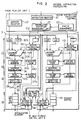
- Fig. 3 shows a detail of the access instruction control unit 33 and the serialization instruction buffer 31.
- An activation signal 210 sent from an instruction activation management unit 21 of the vector instruction execution control unit 2 sets a busy latch 60, for indicating that an access instruction is now under processing, via an AND gate 55 and an OR gate 56 unless the access instruction control unit 33 is not operated.
- the code representative of the type of an access request and the vector length thereof affixed to the activation signal 210 are set in registers 58 and 59, respectively.
- the value in the vector length register 59 is compared by a comparator 63 with the value of a counter 62 which counts the number of delivered access requests or calculation instructions 330 via an + 1 adder 61.
- an instruction processing end notice signal 332 is delivered to the vector instruction execution control unit 2 and the busy latch 60 is reset and the execution vector length value of the counter 62 is initialized to "0".
- a buffer counter 65 is initially reset at "0".
- a comparator 66 compares the value of the buffer counter 65 and the number of registers (four in this embodiment shown in Fig. 2) in the request buffer 39.
- the delivery of an access request 330 is inhibited by an AND gate 68 via an inverter 67.
- a signal 340 indicating that an access request has been delivered to the main storage control unit, is sent from the access request delivery control unit 34, the number of access requests is decremented by 1 by the adder 64.
- Fig. 4 shows a detail of the access request delivery control unit 34 and the serialization unit 10, and a part of the access request delivery control unit 44.
- the corresponding code, address, data and the like are set at the request buffer 39.
- the buffer position is designated by a signal obtained by decoding the value in an in-pointer register 81 by a decoder 88, the value being incremented by + 1 at an adder 80 every time an access request 343 is received.
- the in-pointer 81 takes a value of "0" to "3", "3" being followed by "0" in a lap-around manner.
- the outputted access request 341 is not necessarily accepted by the main storage control unit 8 depending upon the status of the main storage or the contention with another access request.
- an accept signal 345 of such effect is returned.
- the value of an out-pointer 83 is added by "+1" by the adder 82, and a signal 340 indicating that an access request has been processed once is informed to the access instruction control circuit 33.
- the value of the out-pointer 83 takes “0" to "3" similarly to the inpointer 81.
- the code of an access request taken out from the request buffer 39 is decoded by a decoder 84 and if the decoded result shows that the access request is for a serialization instruction, the delivery of an access request from the AND gate 86 is inhibited by a signal from an inverter 85. Thus, the delivery of an access request from the access instruction processing unit 3 is stopped. A signal indicating that a serialization instruction has been detected is also sent to the serialization control circuit 10, i.e., to an AND gate 99. The delivery of the access request from the access instruction processing unit 3 is inhibited until a serialization instruction is detected by the decoder 95 in the access request delivery control unit of the access instruction processing unit 4.
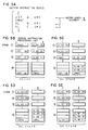
- Figs. 5A to 5F show a series of vector instructions used in the following description, and the sequential status of each element of a vector instruction at stages (1) to (4) in the access instruction processing unit.
- the stage (4) is represented by four first-in and first-out buffers.
- a VST instruction is an instruction for writing data of a vector register "VRO" into a region "A" in the main storage
- a VWAC instruction is an instruction for serializing instructions after and before this instruction
- a VL instruction is an instruction for fetching data in a region "B” or “C” from the main storage to a vector register "VR1" or “VR2”.
- the vector length of respective VST and VL instructions is 8 (element number 1 to 8).
- the number in the parentheses indicates the element number processed at each instruction.
- the mnemonic in each block represents the following instruction: VST ... VST A, VR0 VL(B)... VL B, VR1 VL(C)... VL C, VR2
- the designation of respective regions A, B and C is obtained by a combination of start address A0, B0, C0 and address increments A1, B1, C1 (e.g., VST A0, A1, VR0).
- the instruction activation management unit 21 decodes the instruction to issue it to the access instruction processing unit 3 based on the status of the status management unit 22.
- the instruction activation management unit 21 issues the instruction to both the access instruction processing units 3 and 4. Since the access instruction processing unit 3 is executing the advancing instruction "VST A, VR0", the instruction "VWAC” is set at the serialization instruction buffer 31. After an access request of the advancing instruction has completed, the instruction "VWAC" is moved from the buffer 31 to the access instruction control unit 33 and processed thereat.
- the status (I) shown in Fig. 5B indicates that the above three instructions have been issued and the element of the instruction "VWAC" is present at stage (1) in the access instruction processing unit I.
- the access instructed processing unit I is allowed to receive a next access instruction so that the instruction activation engagement unit 2 of the vector instruction execution control unit 2 issues the held instruction "VL C, VR2" to the access instruction processing unit I.
- the status (II) shown in Fig. 5C represents the status two machine cycles after the status (I). Since the element of the instruction "VWAC" is present at the outlet of the stage (4) of the access request buffer 44, the access instruction processing unit II is caused to inhibit the delivery of an access request, thus holding the access requests in the buffer. The access instruction control unit 43 never outputs access requests in excess of four, so that the fourth element of the access request for the instruction "VL B, VR1" is not still outputted, thereby making the stages (1) and (2) empty.
- the status (III) shown in Fig. 5D represents the status one machine cycle after the status (II). Both the access instruction processing units I and II have the instruction element of "VWAC" at the outlets of the access request buffers. This status is detected by the serialization circuit 10 to increment the out-pointers of both the access control units 34 and 44 by one.
- the status (IV) shown in Fig. 5E represents the status one machine cycle after the status (III). Both the instruction elements "VWAC" are taken out from both the access request buffers 39 and 49 at the same time so that access request elements of the instructions after the serialization instruction are allowed to be delivered.
- the access requests of access instructions after the instruction "VWAC” are caused to be inhibited until all the elements of instructions issued before the instruction "VWAC”, thus enabling a serialization of the instruction "VWAC”.
Landscapes
- Engineering & Computer Science (AREA)
- Theoretical Computer Science (AREA)
- Software Systems (AREA)
- Physics & Mathematics (AREA)
- General Engineering & Computer Science (AREA)
- General Physics & Mathematics (AREA)
- Computer Hardware Design (AREA)
- Computing Systems (AREA)
- Complex Calculations (AREA)
- Advance Control (AREA)
Claims (2)
- Vektorprozessor für die Vektorisierung von Vektordaten, wobei ein Serialisierungsbefehl eingefügt werden kann und der besagte Vektorprozessor eine Vektorbefehl-Ausführungssteuereinheit (2) für die Verteilung von Zugriffsbefehlen und besagten Serialisierungsbefehlen zum Serialisieren der besagten Zugriffsbefehle hat, eine Vielzahl von Zugriffsbefehlleitungen (3, 4), die auf besagte Zugriffsbefehle und Serialisierungsbefehle reagieren, eine Speichereinheit (9) und eine Speichersteuereinheit (8), die auf besagte Zugriffsbefehle zur Steuerung der besagten Speichereinheit reagiert,
dadurch gekennzeichnet, daß die besagte Vektorbefehl-Ausführungssteuereinheit (2) jeden Serialisierungsbefehl an alle der besagten Zugriffsbefehlleitungen weiterleitet und dadurch, daß jede der besagten Zugriffsbefehlleitungen (3, 4) umfaßt:a) eine Adreßerzeugungsvorrichtung (30, 32) für die sequentielle Erzeugung von Adressen, die den besagten Zugriffsbefehlen entsprechen, die durch die besagte Vektorbefehl-Ausführungssteuereinheit verteilt wurden;b) eine Zugriffsbefehl-Steuervorrichtung (33), die auf die besagten Befehle zur Steuerung der besagten Adreßerzeugungsvorrichtung reagiert und Zugriffsanforderungen erzeugt, die den besagten Zugriffsbefehlen entsprechen;c) eine Vielzahl von Anforderungspuffern (39), die auf die besagten Befehle reagieren und die besagten Zugriffsanforderungen mit den besagten Adressen und besagten Serialisierungsbefehlen zwischenspeichern für die sequentielle Weiterleitung an die besagte Speichersteuereinheit (8); undd) Zugriffszulassungsteuervorrichtung (34) für die Steuerung einer Absendung von besagten Zugriffsanforderungen und besagten Adressen an die besagte Speichersteuereinheit, wobei die besagte Zugriffszulassungssteuervorrichtung eine erste Vorrichtung (84, 85, 86) umfaßt, die auf den Inhalt der Vielzahl von Anforderungspuffern reagiert, um das Absenden der besagten Zugriffsanforderungen und der besagten Adressen an die besagte Speichersteuerungseinheit zu unterdrücken, wenn solch ein Serialisierungsbefehl auf der letzten Stufe der besagten Vielzahl von Puffern (39) erkannt wird, und
der besagte Vektorprozessor umfaßt weiterhin eine Serialisierungssteuervorrichtung (10), die auf den Nachweis von Serialisierungsbefehlen bei allen der ersten Vorrichtungen in der besagten Vielzahl von Zugriffsbefehlsleitungen mit Erzeugung eines Steuersignals für das erneute Starten des Absendens von besagten Zugriffsanforderungen und besagten Adressen, die in der besagten Vielzahl von Anforderungspuffern der besagten Vielzahl von Zugriffsbefehlsleitungen zur besagten Speichersteuereinheit gespeichert sind, reagiert. - Vektorprozessor nach Anspruch 1,
dadurch gekennzeichnet, daß
jede der besagten Zugriffsbefehlsleitungen (3, 4) weiterhin enthält:e) eine Serialisierungsbefehlspuffer (31) zwischen der besagten Vektorbefehl-Ausführungssteuereinheit und der besagten Zugriffsbefehl-Steuervorrichtung für die Zwischenspeicherung der besagten Serialisierungsbefehle, die durch die besagte Vektorbefehl-Ausführungssteuereinheit verteilt werden.
Applications Claiming Priority (2)
| Application Number | Priority Date | Filing Date | Title |
|---|---|---|---|
| JP274398/86 | 1986-11-18 | ||
| JP61274398A JPH06103494B2 (ja) | 1986-11-18 | 1986-11-18 | ベクトル処理装置の制御方式 |
Publications (3)
| Publication Number | Publication Date |
|---|---|
| EP0268264A2 EP0268264A2 (de) | 1988-05-25 |
| EP0268264A3 EP0268264A3 (en) | 1989-11-29 |
| EP0268264B1 true EP0268264B1 (de) | 1994-03-30 |
Family
ID=17541110
Family Applications (1)
| Application Number | Title | Priority Date | Filing Date |
|---|---|---|---|
| EP87116964A Expired - Lifetime EP0268264B1 (de) | 1986-11-18 | 1987-11-17 | Steuerungssystem für ein Vektorprozessor |
Country Status (4)
| Country | Link |
|---|---|
| US (1) | US5060148A (de) |
| EP (1) | EP0268264B1 (de) |
| JP (1) | JPH06103494B2 (de) |
| DE (1) | DE3789490T2 (de) |
Families Citing this family (25)
| Publication number | Priority date | Publication date | Assignee | Title |
|---|---|---|---|---|
| US5367654A (en) * | 1988-04-13 | 1994-11-22 | Hitachi Ltd. | Method and apparatus for controlling storage in computer system utilizing forecasted access requests and priority decision circuitry |
| JP2677414B2 (ja) * | 1989-05-15 | 1997-11-17 | 富士通株式会社 | 命令実行のシリアライズ制御方式 |
| JPH03112269U (de) * | 1990-02-28 | 1991-11-18 | ||
| US5257354A (en) * | 1991-01-16 | 1993-10-26 | International Business Machines Corporation | System for monitoring and undoing execution of instructions beyond a serialization point upon occurrence of in-correct results |
| US5590294A (en) * | 1991-03-19 | 1996-12-31 | Silicon Graphics, Inc. | Method and apparatus for retarting pipeline processing |
| US5617575A (en) * | 1991-03-19 | 1997-04-01 | Hitachi, Ltd. | Interprocessor priority control system for multivector processor |
| JP3304444B2 (ja) * | 1992-11-30 | 2002-07-22 | 富士通株式会社 | ベクトル処理装置 |
| JPH06168263A (ja) * | 1992-11-30 | 1994-06-14 | Fujitsu Ltd | ベクトル処理装置 |
| US5542061A (en) * | 1993-01-21 | 1996-07-30 | Nec Corporaiton | Arrangement of controlling issue timing of a read instruction to a common block in a vector processor |
| TW353732B (en) * | 1994-03-31 | 1999-03-01 | Ibm | Processing system and method of operation |
| US5691920A (en) * | 1995-10-02 | 1997-11-25 | International Business Machines Corporation | Method and system for performance monitoring of dispatch unit efficiency in a processing system |
| US5797019A (en) * | 1995-10-02 | 1998-08-18 | International Business Machines Corporation | Method and system for performance monitoring time lengths of disabled interrupts in a processing system |
| US5752062A (en) * | 1995-10-02 | 1998-05-12 | International Business Machines Corporation | Method and system for performance monitoring through monitoring an order of processor events during execution in a processing system |
| US5949971A (en) * | 1995-10-02 | 1999-09-07 | International Business Machines Corporation | Method and system for performance monitoring through identification of frequency and length of time of execution of serialization instructions in a processing system |
| US5748855A (en) * | 1995-10-02 | 1998-05-05 | Iinternational Business Machines Corporation | Method and system for performance monitoring of misaligned memory accesses in a processing system |
| US5729726A (en) * | 1995-10-02 | 1998-03-17 | International Business Machines Corporation | Method and system for performance monitoring efficiency of branch unit operation in a processing system |
| US5751945A (en) * | 1995-10-02 | 1998-05-12 | International Business Machines Corporation | Method and system for performance monitoring stalls to identify pipeline bottlenecks and stalls in a processing system |
| US6389482B1 (en) | 1997-08-28 | 2002-05-14 | International Business Machines Corp. | Dynamic transitioning from a local pipe to a cross-system pipe |
| US6088791A (en) * | 1998-04-30 | 2000-07-11 | International Business Machines Corporation | Computer processor system for implementing the ESA/390 STOSM and STNSM instructions without serialization or artificially extending processor execution time |
| US6088792A (en) * | 1998-04-30 | 2000-07-11 | International Business Machines Corporation | Avoiding processor serialization after an S/390 SPKA instruction |
| JP3344345B2 (ja) | 1998-12-15 | 2002-11-11 | 日本電気株式会社 | 共有メモリ型ベクトル処理システムとその制御方法及びベクトル処理の制御プログラムを格納する記憶媒体 |
| US6665749B1 (en) * | 1999-08-17 | 2003-12-16 | Nec Electronics, Inc. | Bus protocol for efficiently transferring vector data |
| US7644255B2 (en) * | 2005-01-13 | 2010-01-05 | Sony Computer Entertainment Inc. | Method and apparatus for enable/disable control of SIMD processor slices |
| JP2009054032A (ja) * | 2007-08-28 | 2009-03-12 | Toshiba Corp | 並列プロセッサ |
| CN119473932A (zh) * | 2023-07-28 | 2025-02-18 | 深圳市中兴微电子技术有限公司 | 缓存、数据处理装置及芯片 |
Family Cites Families (13)
| Publication number | Priority date | Publication date | Assignee | Title |
|---|---|---|---|---|
| US3651482A (en) * | 1968-04-03 | 1972-03-21 | Honeywell Inc | Interlocking data subprocessors |
| US4101960A (en) * | 1977-03-29 | 1978-07-18 | Burroughs Corporation | Scientific processor |
| US4412303A (en) * | 1979-11-26 | 1983-10-25 | Burroughs Corporation | Array processor architecture |
| JPS6043535B2 (ja) * | 1979-12-29 | 1985-09-28 | 富士通株式会社 | 情報処理装置 |
| JPS5725069A (en) * | 1980-07-21 | 1982-02-09 | Hitachi Ltd | Vector data processing equipment |
| JPS58114274A (ja) * | 1981-12-28 | 1983-07-07 | Hitachi Ltd | デ−タ処理装置 |
| JPS58219646A (ja) * | 1982-06-14 | 1983-12-21 | Hitachi Ltd | パイプライン制御方式 |
| US4569034A (en) * | 1982-07-19 | 1986-02-04 | International Business Machines Corporation | Method and apparatus which allows the working storage to be reconfigured according to demands for processing data input |
| JPS59125472A (ja) * | 1982-12-30 | 1984-07-19 | Fujitsu Ltd | 逐次化命令実行制御装置 |
| ATE154151T1 (de) * | 1983-04-25 | 1997-06-15 | Cray Research Inc | Mehrprozessorsteuerung für vektorrechner |
| DE3374238D1 (en) * | 1983-07-08 | 1987-12-03 | Ibm | A synchronisation mechanism for a multiprocessing system |
| JPS6072069A (ja) * | 1983-09-28 | 1985-04-24 | Nec Corp | ベクトル演算処理装置 |
| US4789925A (en) * | 1985-07-31 | 1988-12-06 | Unisys Corporation | Vector data logical usage conflict detection |
-
1986
- 1986-11-18 JP JP61274398A patent/JPH06103494B2/ja not_active Expired - Lifetime
-
1987
- 1987-11-16 US US07/121,134 patent/US5060148A/en not_active Expired - Lifetime
- 1987-11-17 EP EP87116964A patent/EP0268264B1/de not_active Expired - Lifetime
- 1987-11-17 DE DE3789490T patent/DE3789490T2/de not_active Expired - Fee Related
Also Published As
| Publication number | Publication date |
|---|---|
| EP0268264A3 (en) | 1989-11-29 |
| JPS63127368A (ja) | 1988-05-31 |
| DE3789490T2 (de) | 1994-10-27 |
| EP0268264A2 (de) | 1988-05-25 |
| DE3789490D1 (de) | 1994-05-05 |
| JPH06103494B2 (ja) | 1994-12-14 |
| US5060148A (en) | 1991-10-22 |
Similar Documents
| Publication | Publication Date | Title |
|---|---|---|
| US5060148A (en) | Control system for vector processor with serialization instruction for memory accesses for pipeline operation | |
| US4636942A (en) | Computer vector multiprocessing control | |
| US5185868A (en) | Apparatus having hierarchically arranged decoders concurrently decoding instructions and shifting instructions not ready for execution to vacant decoders higher in the hierarchy | |
| US4395757A (en) | Process synchronization utilizing semaphores | |
| US4752873A (en) | Data processor having a plurality of operating units, logical registers, and physical registers for parallel instructions execution | |
| US5251306A (en) | Apparatus for controlling execution of a program in a computing device | |
| US4369494A (en) | Apparatus and method for providing synchronization between processes and events occurring at different times in a data processing system | |
| US4316245A (en) | Apparatus and method for semaphore initialization in a multiprocessing computer system for process synchronization | |
| US5127091A (en) | System for reducing delay in instruction execution by executing branch instructions in separate processor while dispatching subsequent instructions to primary processor | |
| EP0437044B1 (de) | Datenverarbeitungssystem mit Vorrichtung zur Befehlskennzeichnung | |
| US4394725A (en) | Apparatus and method for transferring information units between processes in a multiprocessing system | |
| US4901230A (en) | Computer vector multiprocessing control with multiple access memory and priority conflict resolution method | |
| US4374409A (en) | Method of and system using P and V instructions on semaphores for transferring data among processes in a multiprocessing system | |
| US5341482A (en) | Method for synchronization of arithmetic exceptions in central processing units having pipelined execution units simultaneously executing instructions | |
| US4320455A (en) | Queue structure for a data processing system | |
| US4745547A (en) | Vector processing | |
| EP0365188B1 (de) | Verfahren und Vorrichtung für Zustandskode in einem Zentralprozessor | |
| US4989133A (en) | System for executing, scheduling, and selectively linking time dependent processes based upon scheduling time thereof | |
| EP0021399A1 (de) | Verfahren und Maschine für Mehrfachbefehlsausführung | |
| EP0042442A1 (de) | Informationsverarbeitende anlage | |
| EP0389001B1 (de) | Mehrprozessorsteuerung für Vektorrechner | |
| GB2159309A (en) | Vector processor | |
| EP0180725A2 (de) | Vorausschauende Speicherabrufoperation für Verzweigungsbefehle | |
| JPH02224055A (ja) | 命令の多機能ユニットへの同時ディスパッチのための方法及び装置 | |
| US5497496A (en) | Superscalar processor controlling fetching of instructions based upon number of empty instructions registers detected for each cycle |
Legal Events
| Date | Code | Title | Description |
|---|---|---|---|
| PUAI | Public reference made under article 153(3) epc to a published international application that has entered the european phase |
Free format text: ORIGINAL CODE: 0009012 |
|
| AK | Designated contracting states |
Kind code of ref document: A2 Designated state(s): DE FR GB |
|
| PUAL | Search report despatched |
Free format text: ORIGINAL CODE: 0009013 |
|
| AK | Designated contracting states |
Kind code of ref document: A3 Designated state(s): DE FR GB |
|
| 17P | Request for examination filed |
Effective date: 19891109 |
|
| 17Q | First examination report despatched |
Effective date: 19920313 |
|
| GRAA | (expected) grant |
Free format text: ORIGINAL CODE: 0009210 |
|
| AK | Designated contracting states |
Kind code of ref document: B1 Designated state(s): DE FR GB |
|
| REF | Corresponds to: |
Ref document number: 3789490 Country of ref document: DE Date of ref document: 19940505 |
|
| ET | Fr: translation filed | ||
| PLBE | No opposition filed within time limit |
Free format text: ORIGINAL CODE: 0009261 |
|
| STAA | Information on the status of an ep patent application or granted ep patent |
Free format text: STATUS: NO OPPOSITION FILED WITHIN TIME LIMIT |
|
| 26N | No opposition filed | ||
| REG | Reference to a national code |
Ref country code: GB Ref legal event code: IF02 |
|
| PGFP | Annual fee paid to national office [announced via postgrant information from national office to epo] |
Ref country code: GB Payment date: 20031104 Year of fee payment: 17 |
|
| PGFP | Annual fee paid to national office [announced via postgrant information from national office to epo] |
Ref country code: FR Payment date: 20031106 Year of fee payment: 17 |
|
| PGFP | Annual fee paid to national office [announced via postgrant information from national office to epo] |
Ref country code: DE Payment date: 20031203 Year of fee payment: 17 |
|
| PG25 | Lapsed in a contracting state [announced via postgrant information from national office to epo] |
Ref country code: GB Free format text: LAPSE BECAUSE OF NON-PAYMENT OF DUE FEES Effective date: 20041117 |
|
| PG25 | Lapsed in a contracting state [announced via postgrant information from national office to epo] |
Ref country code: DE Free format text: LAPSE BECAUSE OF NON-PAYMENT OF DUE FEES Effective date: 20050601 |
|
| GBPC | Gb: european patent ceased through non-payment of renewal fee |
Effective date: 20041117 |
|
| PG25 | Lapsed in a contracting state [announced via postgrant information from national office to epo] |
Ref country code: FR Free format text: LAPSE BECAUSE OF NON-PAYMENT OF DUE FEES Effective date: 20050729 |
|
| REG | Reference to a national code |
Ref country code: FR Ref legal event code: ST |