EP0269095A2 - Circuit intégré à semi-conducteur ayant au moins deux plans métallisés en aluminium ou en alliage d'aluminium ainsi que son procédé de fabrication - Google Patents
Circuit intégré à semi-conducteur ayant au moins deux plans métallisés en aluminium ou en alliage d'aluminium ainsi que son procédé de fabrication Download PDFInfo
- Publication number
- EP0269095A2 EP0269095A2 EP87117415A EP87117415A EP0269095A2 EP 0269095 A2 EP0269095 A2 EP 0269095A2 EP 87117415 A EP87117415 A EP 87117415A EP 87117415 A EP87117415 A EP 87117415A EP 0269095 A2 EP0269095 A2 EP 0269095A2
- Authority
- EP
- European Patent Office
- Prior art keywords
- layer
- tungsten
- titanium
- aluminum
- metallization
- Prior art date
- Legal status (The legal status is an assumption and is not a legal conclusion. Google has not performed a legal analysis and makes no representation as to the accuracy of the status listed.)
- Granted
Links
Images
Classifications
-
- H—ELECTRICITY
- H10—SEMICONDUCTOR DEVICES; ELECTRIC SOLID-STATE DEVICES NOT OTHERWISE PROVIDED FOR
- H10W—GENERIC PACKAGES, INTERCONNECTIONS, CONNECTORS OR OTHER CONSTRUCTIONAL DETAILS OF DEVICES COVERED BY CLASS H10
- H10W20/00—Interconnections in chips, wafers or substrates
- H10W20/01—Manufacture or treatment
- H10W20/031—Manufacture or treatment of conductive parts of the interconnections
- H10W20/032—Manufacture or treatment of conductive parts of the interconnections of conductive barrier, adhesion or liner layers
- H10W20/042—Manufacture or treatment of conductive parts of the interconnections of conductive barrier, adhesion or liner layers the barrier, adhesion or liner layers being seed or nucleation layers
-
- H—ELECTRICITY
- H10—SEMICONDUCTOR DEVICES; ELECTRIC SOLID-STATE DEVICES NOT OTHERWISE PROVIDED FOR
- H10D—INORGANIC ELECTRIC SEMICONDUCTOR DEVICES
- H10D64/00—Electrodes of devices having potential barriers
- H10D64/01—Manufacture or treatment
- H10D64/011—Manufacture or treatment of electrodes ohmically coupled to a semiconductor
- H10D64/0111—Manufacture or treatment of electrodes ohmically coupled to a semiconductor to Group IV semiconductors
- H10D64/0112—Manufacture or treatment of electrodes ohmically coupled to a semiconductor to Group IV semiconductors using conductive layers comprising silicides
-
- H—ELECTRICITY
- H10—SEMICONDUCTOR DEVICES; ELECTRIC SOLID-STATE DEVICES NOT OTHERWISE PROVIDED FOR
- H10W—GENERIC PACKAGES, INTERCONNECTIONS, CONNECTORS OR OTHER CONSTRUCTIONAL DETAILS OF DEVICES COVERED BY CLASS H10
- H10W20/00—Interconnections in chips, wafers or substrates
- H10W20/01—Manufacture or treatment
- H10W20/031—Manufacture or treatment of conductive parts of the interconnections
- H10W20/032—Manufacture or treatment of conductive parts of the interconnections of conductive barrier, adhesion or liner layers
- H10W20/033—Manufacture or treatment of conductive parts of the interconnections of conductive barrier, adhesion or liner layers in openings in dielectrics
-
- H—ELECTRICITY
- H10—SEMICONDUCTOR DEVICES; ELECTRIC SOLID-STATE DEVICES NOT OTHERWISE PROVIDED FOR
- H10W—GENERIC PACKAGES, INTERCONNECTIONS, CONNECTORS OR OTHER CONSTRUCTIONAL DETAILS OF DEVICES COVERED BY CLASS H10
- H10W20/00—Interconnections in chips, wafers or substrates
- H10W20/01—Manufacture or treatment
- H10W20/031—Manufacture or treatment of conductive parts of the interconnections
- H10W20/032—Manufacture or treatment of conductive parts of the interconnections of conductive barrier, adhesion or liner layers
- H10W20/033—Manufacture or treatment of conductive parts of the interconnections of conductive barrier, adhesion or liner layers in openings in dielectrics
- H10W20/036—Manufacture or treatment of conductive parts of the interconnections of conductive barrier, adhesion or liner layers in openings in dielectrics the barrier, adhesion or liner layers being within a main fill metal
-
- H—ELECTRICITY
- H10—SEMICONDUCTOR DEVICES; ELECTRIC SOLID-STATE DEVICES NOT OTHERWISE PROVIDED FOR
- H10W—GENERIC PACKAGES, INTERCONNECTIONS, CONNECTORS OR OTHER CONSTRUCTIONAL DETAILS OF DEVICES COVERED BY CLASS H10
- H10W20/00—Interconnections in chips, wafers or substrates
- H10W20/01—Manufacture or treatment
- H10W20/031—Manufacture or treatment of conductive parts of the interconnections
- H10W20/032—Manufacture or treatment of conductive parts of the interconnections of conductive barrier, adhesion or liner layers
- H10W20/038—Manufacture or treatment of conductive parts of the interconnections of conductive barrier, adhesion or liner layers covering conductive structures
-
- H—ELECTRICITY
- H10—SEMICONDUCTOR DEVICES; ELECTRIC SOLID-STATE DEVICES NOT OTHERWISE PROVIDED FOR
- H10W—GENERIC PACKAGES, INTERCONNECTIONS, CONNECTORS OR OTHER CONSTRUCTIONAL DETAILS OF DEVICES COVERED BY CLASS H10
- H10W20/00—Interconnections in chips, wafers or substrates
- H10W20/01—Manufacture or treatment
- H10W20/031—Manufacture or treatment of conductive parts of the interconnections
- H10W20/056—Manufacture or treatment of conductive parts of the interconnections by filling conductive material into holes, grooves or trenches
-
- H—ELECTRICITY
- H10—SEMICONDUCTOR DEVICES; ELECTRIC SOLID-STATE DEVICES NOT OTHERWISE PROVIDED FOR
- H10W—GENERIC PACKAGES, INTERCONNECTIONS, CONNECTORS OR OTHER CONSTRUCTIONAL DETAILS OF DEVICES COVERED BY CLASS H10
- H10W20/00—Interconnections in chips, wafers or substrates
- H10W20/01—Manufacture or treatment
- H10W20/031—Manufacture or treatment of conductive parts of the interconnections
- H10W20/062—Manufacture or treatment of conductive parts of the interconnections by smoothing of conductive parts, e.g. by planarisation
-
- H—ELECTRICITY
- H10—SEMICONDUCTOR DEVICES; ELECTRIC SOLID-STATE DEVICES NOT OTHERWISE PROVIDED FOR
- H10W—GENERIC PACKAGES, INTERCONNECTIONS, CONNECTORS OR OTHER CONSTRUCTIONAL DETAILS OF DEVICES COVERED BY CLASS H10
- H10W20/00—Interconnections in chips, wafers or substrates
- H10W20/40—Interconnections external to wafers or substrates, e.g. back-end-of-line [BEOL] metallisations or vias connecting to gate electrodes
- H10W20/41—Interconnections external to wafers or substrates, e.g. back-end-of-line [BEOL] metallisations or vias connecting to gate electrodes characterised by their conductive parts
- H10W20/42—Vias, e.g. via plugs
-
- H—ELECTRICITY
- H10—SEMICONDUCTOR DEVICES; ELECTRIC SOLID-STATE DEVICES NOT OTHERWISE PROVIDED FOR
- H10W—GENERIC PACKAGES, INTERCONNECTIONS, CONNECTORS OR OTHER CONSTRUCTIONAL DETAILS OF DEVICES COVERED BY CLASS H10
- H10W20/00—Interconnections in chips, wafers or substrates
- H10W20/40—Interconnections external to wafers or substrates, e.g. back-end-of-line [BEOL] metallisations or vias connecting to gate electrodes
- H10W20/41—Interconnections external to wafers or substrates, e.g. back-end-of-line [BEOL] metallisations or vias connecting to gate electrodes characterised by their conductive parts
- H10W20/425—Barrier, adhesion or liner layers
Definitions
- the invention relates to an integrated semiconductor circuit with a substrate consisting of silicon, in and on which the elements forming the circuit are produced, and with at least two metallization levels consisting of aluminum or an aluminum compound, separated by an insulation layer, which are made using metal silicide intermediate layers and contact hole fillers consisting of tungsten are connected among themselves and with the areas to be contacted in and on the silicon substrate.
- the insulation layer must have a minimum thickness of 0.7 to 1.5 ⁇ m due to circuitry considerations (for example parasitic capacitances), depth / diameter ratios of greater than / equal to 1 occur in the contact holes or via holes.
- the layer thickness of the interconnects on the flanks of the contact hole decreases very significantly (55 to 80% decrease) if the interconnect material is, for example, aluminum alloys: aluminum-silicon (1%), as was previously the case by sputtering ) is applied.
- each cross-sectional narrowing causes a local temperature rise, which accelerates undesired material transport (diffusion, reaction) at the interfaces between the different materials in contact. This can also lead to the burnout of an interconnect.
- Another problem is that cavities can form in the contact holes after coating, for example with aluminum-silicon. If an insulation layer is then subsequently deposited, for example as a base for a further aluminum-silicon interconnect level, it is practically not possible to remove the one in the contact hole Completely fill the cavity. Since reactive or corrosive media can accumulate in this cavity during further production steps, it is necessary for reliable components to specify a contact hole or via-hole metallization scheme in which complete filling takes place.
- a similar contact hole filling method is proposed in European Patent Application No. 86 10 28 21.5, aluminum being used instead of the silicides and high-melting metals, which is deposited over the entire surface by low pressure gas phase deposition (LPCVD) and etched back to the contact hole height.
- LPCVD low pressure gas phase deposition
- An integrated semiconductor circuit with an outer interconnect level consisting of aluminum or an aluminum compound, in which a metal silicide intermediate layer made of tantalum disilicide has been deposited in order to improve the current load in the contact hole, is known from European patent application 0 132 720.
- German patent application P 36 15 893.3 has also already proposed to use tungsten to fill contact holes in insulation layers of integrated semiconductor circuits. Due to the good edge coverage of the CVD process, the layer in the contact hole grows approximately equally quickly from all sides and fills the contact hole.
- cover layers consist of molybdenum silicide (MoSi2) and the seeding layers consist of a double layer made of titanium / titanium nitride.
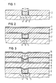
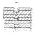
- FIGS. 1 to 4 represent the essential method steps for producing the metallization system according to the invention in the sectional view.
- the same reference numerals apply to the same parts in all figures.
- a SiO 2 layer 2 serving as the first insulation layer is applied, into which the contact hole 3 with a diameter of approximately 0.8 ⁇ m in the region of diffused area 4 in the silicon substrate 1 has been etched.
- a double layer 5, 6, consisting of a 10 nm thick tungsten-silicon alloy (1: 2.5) and an 800 nm thick pure tungsten layer 6, is now applied to this arrangement 1, 2, 3, 4 applied by thermal decomposition of tungsten hexafluoride with hydrogen as reaction gas at 450 ° C in a cold wall reactor at low pressure.
- the intermediate layer 5 made of tungsten silicide serves as a diffusion barrier in later temperature steps.
- a tungsten silicide layer (5) a layer of titanium / tungsten (Ti / W), titanium / tungsten nitride (Ti / W: N) or titanium-titanium nitride (Ti / TiN) can also be used, which acts as a diffusion barrier for Si is suitable for later tungsten deposition and subsequent temperature steps and thereby ensures low-resistance contact to the diffused area.
- the tungsten silicide and tungsten layer (5, 6) present on the substrate surface 1 is etched back until only the contact hole (3) remains filled with tungsten (6) .
- the next step is the deposition of a nucleation layer 7 consisting of the combination titanium (20 nm) / titanium nitride (100 nm) for the subsequent application of the first metallization level 8, which is predominantly made of aluminum (for example aluminum / silicon or aluminum / silicon / titanium).
- the first metallization level 8 which is predominantly made of aluminum (for example aluminum / silicon or aluminum / silicon / titanium).
- aluminum on titanium / titanium nitride shows a strong ⁇ 111> texture and very homogeneous crystallite size distribution with suitable production parameters with cathode sputtering or vapor deposition. (high growth rate 20 nm / sec, low residual gas content less than 1.10 ⁇ 6 pa).
- the improvement in the electromigration properties of, for example, an aluminum / copper alloy is not based on the incorporation of intermediate layers, but essentially on the crystallite structure, texture and crystallite size distribution of the aluminum achieved thereby. If the nucleation layer, preferably made of Ti / TiN, has a strong texture, this is also transferred to the aluminum layer. The grain size distribution of the aluminum is determined by the structure of the germination layer and can therefore be adjusted in a targeted manner.
- a cover layer 9 of, for example, molybdenum silicide is applied to the first metallization level 8 in a layer thickness of 100 nm.
- the cover layer 9 can be either from a sintered target or from a composite target (made from parts of silicon and Molybdenum) can be applied by sputtering.
- the triple layer (7, 8, 9) is structured in the conductor pattern; this process is not shown in the figures because it is not essential to the invention.
- the second titanium / titanium nitride layer 17 deposited thereon is produced as described in FIG. 2; the same applies to the second metallization level 18.
- a second cover layer 19, for example made of molybdenum silicide is applied and structured on the second metallization level 18 as described in FIG. 2.
- the cover layers 9 and 19, for example made of molybdenum silicide also serve, among other things, for hillock suppression by forming aluminum-rich aluminum / silicon / molybdenum or aluminum / molybdenum compounds.
- Tensions between the insulation layers (2, 10) and the metallization levels (8, 18) are equalized.
- Reference numeral 20 designates the third insulation layer (SiO x ), 26 the second via-hole filling with tungsten, 27 the third germination layer consisting of titanium / titanium nitride and 28 the third metallization level.
Landscapes
- Internal Circuitry In Semiconductor Integrated Circuit Devices (AREA)
- Semiconductor Integrated Circuits (AREA)
- Electrodes Of Semiconductors (AREA)
Priority Applications (1)
| Application Number | Priority Date | Filing Date | Title |
|---|---|---|---|
| AT87117415T ATE101751T1 (de) | 1986-11-28 | 1987-11-25 | Integrierte halbleiterschaltung mit mindestens zwei aus aluminium oder einer aluminiumverbindung bestehenden metallisierungsebenen sowie verfahren zu ihrer herstellung. |
Applications Claiming Priority (2)
| Application Number | Priority Date | Filing Date | Title |
|---|---|---|---|
| DE3640656 | 1986-11-28 | ||
| DE3640656 | 1986-11-28 |
Publications (3)
| Publication Number | Publication Date |
|---|---|
| EP0269095A2 true EP0269095A2 (fr) | 1988-06-01 |
| EP0269095A3 EP0269095A3 (en) | 1990-08-08 |
| EP0269095B1 EP0269095B1 (fr) | 1994-02-16 |
Family
ID=6314980
Family Applications (1)
| Application Number | Title | Priority Date | Filing Date |
|---|---|---|---|
| EP87117415A Expired - Lifetime EP0269095B1 (fr) | 1986-11-28 | 1987-11-25 | Circuit intégré à semi-conducteur ayant au moins deux plans métallisés en aluminium ou en alliage d'aluminium ainsi que son procédé de fabrication |
Country Status (7)
| Country | Link |
|---|---|
| US (1) | US4924295A (fr) |
| EP (1) | EP0269095B1 (fr) |
| JP (1) | JP2593821B2 (fr) |
| KR (1) | KR910007108B1 (fr) |
| AT (1) | ATE101751T1 (fr) |
| DE (1) | DE3789090D1 (fr) |
| HK (1) | HK167395A (fr) |
Cited By (4)
| Publication number | Priority date | Publication date | Assignee | Title |
|---|---|---|---|---|
| EP0357221A1 (fr) * | 1988-08-01 | 1990-03-07 | AT&T Corp. | Procédé de fabrication de contacts dans des circuits intégrés à jonctions peu profondes |
| EP0451644A1 (fr) * | 1990-04-10 | 1991-10-16 | Texas Instruments Incorporated | Système de métallisation amélioré afin de réduire la sensibilité à la corrosion |
| EP0509835A3 (en) * | 1991-04-19 | 1992-12-23 | Sharp Kabushiki Kaisha | Method for forming contact portion of semiconductor device |
| EP0587400A3 (en) * | 1992-09-11 | 1996-02-07 | Inmos Ltd | Manufacture of interconnections in semiconductor devices |
Families Citing this family (45)
| Publication number | Priority date | Publication date | Assignee | Title |
|---|---|---|---|---|
| CA1306072C (fr) * | 1987-03-30 | 1992-08-04 | John E. Cronin | Structures conductrices composees d'un metal refractaire et d'une mince couche de nitrure de titanium, et procedes de fabrication connexes |
| US5132775A (en) * | 1987-12-11 | 1992-07-21 | Texas Instruments Incorporated | Methods for and products having self-aligned conductive pillars on interconnects |
| JPH01298765A (ja) * | 1988-05-27 | 1989-12-01 | Fujitsu Ltd | 半導体装置及びその製造方法 |
| JPH0235753A (ja) * | 1988-07-26 | 1990-02-06 | Matsushita Electric Ind Co Ltd | 半導体装置の製造方法 |
| JPH0274039A (ja) * | 1988-09-09 | 1990-03-14 | Texas Instr Japan Ltd | 電子回路装置 |
| JP2769331B2 (ja) * | 1988-09-12 | 1998-06-25 | 株式会社日立製作所 | 半導体集積回路の製造方法 |
| JPH02181920A (ja) * | 1989-01-09 | 1990-07-16 | Hitachi Ltd | 半導体集積回路装置 |
| US5157589A (en) * | 1990-07-02 | 1992-10-20 | General Electric Company | Mutliple lamination high density interconnect process and structure employing thermoplastic adhesives having sequentially decreasing TG 's |
| JP2598335B2 (ja) * | 1990-08-28 | 1997-04-09 | 三菱電機株式会社 | 半導体集積回路装置の配線接続構造およびその製造方法 |
| JP2660359B2 (ja) * | 1991-01-30 | 1997-10-08 | 三菱電機株式会社 | 半導体装置 |
| DE69225082T2 (de) * | 1991-02-12 | 1998-08-20 | Matsushita Electronics Corp | Halbleiter-Vorrichtung mit Verdrahtung der verbesserten Zuverlässigkeit und Verfahren zu ihner Herstellung |
| US5270254A (en) * | 1991-03-27 | 1993-12-14 | Sgs-Thomson Microelectronics, Inc. | Integrated circuit metallization with zero contact enclosure requirements and method of making the same |
| JP3099406B2 (ja) * | 1991-04-05 | 2000-10-16 | ヤマハ株式会社 | 集積回路の多層配線構造 |
| JP2811131B2 (ja) * | 1991-04-26 | 1998-10-15 | 三菱電機株式会社 | 半導体装置の配線接続構造およびその製造方法 |
| US5389575A (en) * | 1991-07-12 | 1995-02-14 | Hughes Aircraft Company | Self-aligned contact diffusion barrier method |
| EP0526244B1 (fr) * | 1991-07-31 | 2000-01-05 | STMicroelectronics, Inc. | Procédé de formation d'un contact enterré en silicium polycristallin |
| KR970009274B1 (ko) * | 1991-11-11 | 1997-06-09 | 미쓰비시덴키 가부시키가이샤 | 반도체장치의 도전층접속구조 및 그 제조방법 |
| JPH05198525A (ja) * | 1992-01-21 | 1993-08-06 | Sony Corp | 配線構造及び配線の形成方法 |
| US5300813A (en) * | 1992-02-26 | 1994-04-05 | International Business Machines Corporation | Refractory metal capped low resistivity metal conductor lines and vias |
| JPH05275540A (ja) * | 1992-03-28 | 1993-10-22 | Yamaha Corp | 集積回路装置 |
| US5262352A (en) * | 1992-08-31 | 1993-11-16 | Motorola, Inc. | Method for forming an interconnection structure for conductive layers |
| EP0608628A3 (fr) * | 1992-12-25 | 1995-01-18 | Kawasaki Steel Co | Procédé pour fabriquer un dispositif semi-conducteur ayant une structure d'interconnexion multi-couches. |
| KR970001883B1 (ko) * | 1992-12-30 | 1997-02-18 | 삼성전자 주식회사 | 반도체장치 및 그 제조방법 |
| JP3216345B2 (ja) * | 1993-04-06 | 2001-10-09 | ソニー株式会社 | 半導体装置及びその作製方法 |
| US5937327A (en) * | 1993-04-23 | 1999-08-10 | Ricoh Company, Ltd. | Method for improving wiring contact in semiconductor devices |
| US5589418A (en) * | 1993-08-04 | 1996-12-31 | Sgs-Thomson Microelectronics, Inc. | Method of forming a polysilicon buried contact |
| US5571751A (en) * | 1994-05-09 | 1996-11-05 | National Semiconductor Corporation | Interconnect structures for integrated circuits |
| EP0690503A1 (fr) * | 1994-05-31 | 1996-01-03 | Advanced Micro Devices, Inc. | Structure améliorée d'une ligne d'interconnexion et procédé |
| JPH08130246A (ja) * | 1994-10-28 | 1996-05-21 | Ricoh Co Ltd | 半導体装置とその製造方法 |
| JP2737764B2 (ja) * | 1995-03-03 | 1998-04-08 | 日本電気株式会社 | 半導体装置及びその製造方法 |
| US5563097A (en) * | 1995-04-17 | 1996-10-08 | Lee; Young J. | Method for fabricating semiconductor device |
| US5756396A (en) * | 1996-05-06 | 1998-05-26 | Taiwan Semiconductor Manufacturing Company Ltd | Method of making a multi-layer wiring structure having conductive sidewall etch stoppers and a stacked plug interconnect |
| US20040222525A1 (en) * | 1997-03-14 | 2004-11-11 | Rhodes Howard E. | Advanced VLSI metallization |
| JPH1197525A (ja) * | 1997-09-19 | 1999-04-09 | Hitachi Ltd | 半導体装置およびその製造方法 |
| US5907175A (en) * | 1997-09-25 | 1999-05-25 | Advanced Micro Devices, Inc | Four transistor SRAM cell |
| US6452276B1 (en) * | 1998-04-30 | 2002-09-17 | International Business Machines Corporation | Ultra thin, single phase, diffusion barrier for metal conductors |
| US6562674B1 (en) * | 1999-07-06 | 2003-05-13 | Matsushita Electronics Corporation | Semiconductor integrated circuit device and method of producing the same |
| US6429389B1 (en) * | 2000-11-15 | 2002-08-06 | Intel Corporation | Via-in-pad apparatus and methods |
| JP4965443B2 (ja) * | 2005-06-30 | 2012-07-04 | スパンション エルエルシー | 半導体装置の製造方法 |
| US20080237738A1 (en) * | 2007-03-27 | 2008-10-02 | Christoph Andreas Kleint | Integrated circuit, cell, cell arrangement, method for manufacturing an integrated circuit, method for manufacturing a cell arrangement; memory module |
| JP5369570B2 (ja) * | 2008-09-17 | 2013-12-18 | 株式会社大真空 | 圧電振動デバイスの封止部材の製造方法 |
| US9209109B2 (en) | 2013-07-15 | 2015-12-08 | Infineon Technologies Ag | IGBT with emitter electrode electrically connected with an impurity zone |
| US9337827B2 (en) | 2013-07-15 | 2016-05-10 | Infineon Technologies Ag | Electronic circuit with a reverse-conducting IGBT and gate driver circuit |
| US9812328B2 (en) | 2015-06-22 | 2017-11-07 | Applied Materials, Inc. | Methods for forming low resistivity interconnects |
| US9806041B1 (en) * | 2016-04-22 | 2017-10-31 | Infineon Technologies Ag | Method for processing an electronic component and an electronic component |
Family Cites Families (9)
| Publication number | Priority date | Publication date | Assignee | Title |
|---|---|---|---|---|
| US3614547A (en) * | 1970-03-16 | 1971-10-19 | Gen Electric | Tungsten barrier electrical connection |
| US4107726A (en) * | 1977-01-03 | 1978-08-15 | Raytheon Company | Multilayer interconnected structure for semiconductor integrated circuit |
| JPS5748259A (en) * | 1980-09-05 | 1982-03-19 | Hitachi Ltd | Solid-state image pickup element |
| JPS57208161A (en) * | 1981-06-18 | 1982-12-21 | Fujitsu Ltd | Semiconductor device |
| JPS59175763A (ja) * | 1983-03-25 | 1984-10-04 | Fujitsu Ltd | 半導体装置 |
| JPS60119755A (ja) * | 1983-12-01 | 1985-06-27 | Nec Corp | 多層配線半導体集積回路装置 |
| US4566026A (en) * | 1984-04-25 | 1986-01-21 | Honeywell Inc. | Integrated circuit bimetal layer |
| JPS61174767A (ja) * | 1985-01-30 | 1986-08-06 | Nec Corp | 半導体素子電極 |
| EP0211318B1 (fr) * | 1985-07-29 | 1989-09-27 | Siemens Aktiengesellschaft | Procédé de remplissage sélectif de trous de contact formés par attaque dans des couches d'isolation avec des matériaux électriquement conducteurs pour la fabrication de circuits semi-conducteurs à haute densité d'intégration et appareil utilisé pour ce procédé |
-
1987
- 1987-10-13 US US07/107,344 patent/US4924295A/en not_active Expired - Lifetime
- 1987-11-24 JP JP62295951A patent/JP2593821B2/ja not_active Expired - Lifetime
- 1987-11-25 EP EP87117415A patent/EP0269095B1/fr not_active Expired - Lifetime
- 1987-11-25 DE DE87117415T patent/DE3789090D1/de not_active Expired - Lifetime
- 1987-11-25 AT AT87117415T patent/ATE101751T1/de not_active IP Right Cessation
- 1987-11-28 KR KR1019870013476A patent/KR910007108B1/ko not_active Expired
-
1995
- 1995-10-26 HK HK167395A patent/HK167395A/xx not_active IP Right Cessation
Cited By (4)
| Publication number | Priority date | Publication date | Assignee | Title |
|---|---|---|---|---|
| EP0357221A1 (fr) * | 1988-08-01 | 1990-03-07 | AT&T Corp. | Procédé de fabrication de contacts dans des circuits intégrés à jonctions peu profondes |
| EP0451644A1 (fr) * | 1990-04-10 | 1991-10-16 | Texas Instruments Incorporated | Système de métallisation amélioré afin de réduire la sensibilité à la corrosion |
| EP0509835A3 (en) * | 1991-04-19 | 1992-12-23 | Sharp Kabushiki Kaisha | Method for forming contact portion of semiconductor device |
| EP0587400A3 (en) * | 1992-09-11 | 1996-02-07 | Inmos Ltd | Manufacture of interconnections in semiconductor devices |
Also Published As
| Publication number | Publication date |
|---|---|
| KR910007108B1 (ko) | 1991-09-18 |
| DE3789090D1 (de) | 1994-03-24 |
| KR880006771A (ko) | 1988-07-25 |
| HK167395A (en) | 1995-11-03 |
| JP2593821B2 (ja) | 1997-03-26 |
| JPS63142835A (ja) | 1988-06-15 |
| EP0269095B1 (fr) | 1994-02-16 |
| US4924295A (en) | 1990-05-08 |
| ATE101751T1 (de) | 1994-03-15 |
| EP0269095A3 (en) | 1990-08-08 |
Similar Documents
| Publication | Publication Date | Title |
|---|---|---|
| EP0269095B1 (fr) | Circuit intégré à semi-conducteur ayant au moins deux plans métallisés en aluminium ou en alliage d'aluminium ainsi que son procédé de fabrication | |
| DE3851163T2 (de) | Kontakt in einer Bohrung in einem Halbleiter und Verfahren zu seiner Herstellung. | |
| DE4342047B4 (de) | Halbleiterbauelement mit einer Diffusionsbarrierenschichtanordnung und Verfahren zu seiner Herstellung | |
| DE69836114T2 (de) | Kupferverdrahtung mit verbessertem Elektromigrationswiderstand und reduzierter Defektempfindlichkeit | |
| DE69616081T2 (de) | Verbindungsschema für integrierte schaltungen | |
| DE68918773T2 (de) | Verfahren zur Herstellung einer Halbleitervorrichtung mit mindestens einer kleine Kontaktlöcher enthaltenden Leiterbahn. | |
| DE69517295T2 (de) | Weicher Metallleiter und Herstellungsverfahren | |
| DE4200809C2 (de) | Verfahren zur Bildung einer metallischen Verdrahtungsschicht in einem Halbleiterbauelement | |
| DE69225082T2 (de) | Halbleiter-Vorrichtung mit Verdrahtung der verbesserten Zuverlässigkeit und Verfahren zu ihner Herstellung | |
| DE69314679T2 (de) | Mit schwerschmelzendem Metal abgedeckte metallische Leiterbahnen und Kontaktlöcher | |
| DE69226133T2 (de) | Verbindungsstruktur einer Halbleiteranordnung und ein Herstellungsverfahren dafür | |
| DE69625265T2 (de) | Halbleiterstrukturen | |
| DE3782904T2 (de) | Verfahren zur ausbildung einer kupfer enthaltenden metallisierungsschicht auf der oberflaeche eines halbleiterbauelementes. | |
| DE69231389T2 (de) | Verfahren zur Herstellung eines elektrischer Kontaktes über einem Silizium-Halbleiterplättchen | |
| DE69329663T2 (de) | Verfahren zur Herstellung einer konformen Feuerfestmetallschicht in einer submikronischen Öffnung | |
| DE112006000465B4 (de) | Halbleiterbauelemente mit Barriereschichten für leitende Strukturmerkmale sowie zugehörige Herstellungsverfahren | |
| EP0132720B1 (fr) | Circuit semi-conducteur intégré comprenant une couche de contact et d'interconnexion extérieure en aluminium ou en un alliage d'aluminium | |
| DE10196065B3 (de) | Verbindungsstruktur für eine integrierte Schaltung, Verfahren zur Herstellung der Verbindungsstruktur und integrierte Schaltung mit der Verbindungsstruktur | |
| EP0304728A2 (fr) | Procédé de fabrication d'une métallisation plane de faible résistance en aluminium ou en alliage d'aluminium | |
| DE69015564T2 (de) | Vollverdiefte verbindungsstruktur mit titanium/wolfram und selektivem cvd-wolfram. | |
| EP0199078A1 (fr) | Circuit intégré à semi-conducteur comprenant une voie conductrice de contact en aluminium ou en alliage d'aluminium et une couche intermédiaire en siliciure de tantale comme barrière de diffusion | |
| DE69428113T2 (de) | Verfahren zum planarisieren von submikrondurchgängen und herstellung integrierter halbleiterschaltungen | |
| DE3414781A1 (de) | Vielschicht-verbindungsstruktur einer halbleitereinrichtung | |
| DE19608208A1 (de) | Verfahren zur Herstellung von Metallzwischenverbindungen in Halbleitereinrichtungen | |
| DE10146359A1 (de) | Ein Metallisierungsprozesssequenz |
Legal Events
| Date | Code | Title | Description |
|---|---|---|---|
| PUAI | Public reference made under article 153(3) epc to a published international application that has entered the european phase |
Free format text: ORIGINAL CODE: 0009012 |
|
| AK | Designated contracting states |
Kind code of ref document: A2 Designated state(s): AT BE CH DE FR GB IT LI NL |
|
| PUAL | Search report despatched |
Free format text: ORIGINAL CODE: 0009013 |
|
| AK | Designated contracting states |
Kind code of ref document: A3 Designated state(s): AT BE CH DE FR GB IT LI NL |
|
| 17P | Request for examination filed |
Effective date: 19900919 |
|
| 17Q | First examination report despatched |
Effective date: 19910724 |
|
| GRAA | (expected) grant |
Free format text: ORIGINAL CODE: 0009210 |
|
| AK | Designated contracting states |
Kind code of ref document: B1 Designated state(s): AT BE CH DE FR GB IT LI NL |
|
| REF | Corresponds to: |
Ref document number: 101751 Country of ref document: AT Date of ref document: 19940315 Kind code of ref document: T |
|
| REF | Corresponds to: |
Ref document number: 3789090 Country of ref document: DE Date of ref document: 19940324 |
|
| ET | Fr: translation filed | ||
| ITF | It: translation for a ep patent filed | ||
| GBT | Gb: translation of ep patent filed (gb section 77(6)(a)/1977) |
Effective date: 19940425 |
|
| PLBE | No opposition filed within time limit |
Free format text: ORIGINAL CODE: 0009261 |
|
| STAA | Information on the status of an ep patent application or granted ep patent |
Free format text: STATUS: NO OPPOSITION FILED WITHIN TIME LIMIT |
|
| 26N | No opposition filed | ||
| PGFP | Annual fee paid to national office [announced via postgrant information from national office to epo] |
Ref country code: AT Payment date: 19951025 Year of fee payment: 9 |
|
| PGFP | Annual fee paid to national office [announced via postgrant information from national office to epo] |
Ref country code: BE Payment date: 19951116 Year of fee payment: 9 |
|
| PGFP | Annual fee paid to national office [announced via postgrant information from national office to epo] |
Ref country code: NL Payment date: 19951117 Year of fee payment: 9 |
|
| PGFP | Annual fee paid to national office [announced via postgrant information from national office to epo] |
Ref country code: CH Payment date: 19960216 Year of fee payment: 9 |
|
| PG25 | Lapsed in a contracting state [announced via postgrant information from national office to epo] |
Ref country code: AT Effective date: 19961125 |
|
| PG25 | Lapsed in a contracting state [announced via postgrant information from national office to epo] |
Ref country code: LI Effective date: 19961130 Ref country code: CH Effective date: 19961130 Ref country code: BE Effective date: 19961130 |
|
| BERE | Be: lapsed |
Owner name: SIEMENS A.G. Effective date: 19961130 |
|
| PG25 | Lapsed in a contracting state [announced via postgrant information from national office to epo] |
Ref country code: NL Effective date: 19970601 |
|
| REG | Reference to a national code |
Ref country code: CH Ref legal event code: PL |
|
| NLV4 | Nl: lapsed or anulled due to non-payment of the annual fee |
Effective date: 19970601 |
|
| REG | Reference to a national code |
Ref country code: GB Ref legal event code: IF02 |
|
| PGFP | Annual fee paid to national office [announced via postgrant information from national office to epo] |
Ref country code: FR Payment date: 20061124 Year of fee payment: 20 |
|
| PGFP | Annual fee paid to national office [announced via postgrant information from national office to epo] |
Ref country code: GB Payment date: 20061127 Year of fee payment: 20 |
|
| PGFP | Annual fee paid to national office [announced via postgrant information from national office to epo] |
Ref country code: IT Payment date: 20061130 Year of fee payment: 20 |
|
| PGFP | Annual fee paid to national office [announced via postgrant information from national office to epo] |
Ref country code: DE Payment date: 20070115 Year of fee payment: 20 |
|
| REG | Reference to a national code |
Ref country code: GB Ref legal event code: PE20 |
|
| PG25 | Lapsed in a contracting state [announced via postgrant information from national office to epo] |
Ref country code: GB Free format text: LAPSE BECAUSE OF EXPIRATION OF PROTECTION Effective date: 20071124 |