EP0269162A1 - Dispositif de filtrage - Google Patents
Dispositif de filtrage Download PDFInfo
- Publication number
- EP0269162A1 EP0269162A1 EP87202138A EP87202138A EP0269162A1 EP 0269162 A1 EP0269162 A1 EP 0269162A1 EP 87202138 A EP87202138 A EP 87202138A EP 87202138 A EP87202138 A EP 87202138A EP 0269162 A1 EP0269162 A1 EP 0269162A1
- Authority
- EP
- European Patent Office
- Prior art keywords
- input
- filter arrangement
- inverting
- resistors
- resistor
- Prior art date
- Legal status (The legal status is an assumption and is not a legal conclusion. Google has not performed a legal analysis and makes no representation as to the accuracy of the status listed.)
- Granted
Links
Images


Classifications
-
- H—ELECTRICITY
- H03—ELECTRONIC CIRCUITRY
- H03H—IMPEDANCE NETWORKS, e.g. RESONANT CIRCUITS; RESONATORS
- H03H11/00—Networks using active elements
- H03H11/02—Multiple-port networks
- H03H11/32—Networks for transforming balanced signals into unbalanced signals and vice versa, e.g. baluns
-
- H—ELECTRICITY
- H03—ELECTRONIC CIRCUITRY
- H03H—IMPEDANCE NETWORKS, e.g. RESONANT CIRCUITS; RESONATORS
- H03H11/00—Networks using active elements
- H03H11/02—Multiple-port networks
- H03H11/04—Frequency selective two-port networks
-
- H—ELECTRICITY
- H03—ELECTRONIC CIRCUITRY
- H03F—AMPLIFIERS
- H03F3/00—Amplifiers with only discharge tubes or only semiconductor devices as amplifying elements
- H03F3/45—Differential amplifiers
- H03F3/45071—Differential amplifiers with semiconductor devices only
- H03F3/45076—Differential amplifiers with semiconductor devices only characterised by the way of implementation of the active amplifying circuit in the differential amplifier
- H03F3/4508—Differential amplifiers with semiconductor devices only characterised by the way of implementation of the active amplifying circuit in the differential amplifier using bipolar transistors as the active amplifying circuit
- H03F3/45085—Long tailed pairs
- H03F3/45089—Non-folded cascode stages
-
- H—ELECTRICITY
- H03—ELECTRONIC CIRCUITRY
- H03F—AMPLIFIERS
- H03F3/00—Amplifiers with only discharge tubes or only semiconductor devices as amplifying elements
- H03F3/45—Differential amplifiers
- H03F3/45071—Differential amplifiers with semiconductor devices only
- H03F3/45076—Differential amplifiers with semiconductor devices only characterised by the way of implementation of the active amplifying circuit in the differential amplifier
- H03F3/45475—Differential amplifiers with semiconductor devices only characterised by the way of implementation of the active amplifying circuit in the differential amplifier using IC blocks as the active amplifying circuit
-
- H—ELECTRICITY
- H03—ELECTRONIC CIRCUITRY
- H03F—AMPLIFIERS
- H03F2203/00—Indexing scheme relating to amplifiers with only discharge tubes or only semiconductor devices as amplifying elements covered by H03F3/00
- H03F2203/45—Indexing scheme relating to differential amplifiers
- H03F2203/45562—Indexing scheme relating to differential amplifiers the IC comprising a cross coupling circuit, e.g. comprising two cross-coupled transistors
-
- H—ELECTRICITY
- H03—ELECTRONIC CIRCUITRY
- H03H—IMPEDANCE NETWORKS, e.g. RESONANT CIRCUITS; RESONATORS
- H03H1/00—Constructional details of impedance networks whose electrical mode of operation is not specified or applicable to more than one type of network
- H03H1/02—RC networks, e.g. filters
Definitions
- the invention relates to a filter arrangement comprising a balanced amplifier having an inverting input, a non-inverting input, an inverting output and a non-inverting output, at least a first input circuit arranged between a first input terminal and the inverting input, at least a second input circuit arranged between a second input terminal and the non-inverting input, a first feedback circuit arranged between the non-inverting output and the inverting input, and a second feedback circuit arranged between the inverting output and the non-inverting input, which first and second input circuit each comprise a substantially identical first circuit element, which first and second feedback circuits each comprise a substantially identical second circuit element, one of said two circuit elements being a capacitor and the other circuit element being a resistor and the magnitude of at least one of said two circuit elements being adjustable.
- Such a filter arrangement may be employed in, for example filters, oscillators and resonators.
- Such a filter arrangement is known from United States Patent Specification 4,509,019.
- one circuit element is constituted by a capacitor having a fixed capacitance and the other circuit element is constituted by a resistor formed by a MOS transistor whose resistance value can be adjusted by means of a control voltage applied to its gate electrode.
- the RC-time constant of the resistor and the capacitor can be adjusted to the desired value.
- the capacitors may be arranged in the feedback circuits and the resistors in the input circuits or the capacitors may be arranged in the input circuits and the resistors in the feedback circuits.
- the filter circuit constitutes an integrator or low-pass filter and in the second case it constitutes a differentiator or high-pass filter.
- a balanced input voltage is applied to the first and the second input terminal of the filter arrangement and a balanced output voltage is available on the inverting and the non-inverting output of the amplifier.
- This output voltage is substantially free of even-order harmonic distortion, which is inter alia caused by non-linearities of the MOS resistors. This is because these harmonic components cancel one another as a result of the symmetrical construction of the arrangement and the balanced drive.
- a drawback of this known arrangement is that it can be realised only by means of a semiconductor process enabling MOS transistors to be fabricated.
- the arrangement cannot be realised by means of a purely bipolar process. Therefore, it is the object of the invention to provide a balanced filter arrangement with a variable RC-time constant which can also be fabricated by means of a bipolar process.
- an arrangement of the type defined in the opening paragraph is characterized in that one element is constituted by a junction capacitor and in that a bias-current source is connected to the inverting input and to the non-inverting input for adjusting the capacitance of the junction capacitor connected to the relevant input.
- junction capacitors whose capacitance can be varied to adjust the time constant of the arrangement.
- junction capacitors are formed by a reverse-biassed semiconductor junction (PN-junction), the capacitance depending on the voltage across this junction.
- this capacitance can be adjusted by means of a bias-current source which produces the bias voltage for the junction capacitor across resistors connected to the relevant input. It has been found that distortions in the arrangement produced as a result of non-linearities of the junction capacitors are compensated for in the same way as those caused by the MOS resistors in the known arrangement.
- the invention is not limited to a filter arrangement which can be fabricated exclusively by means of a bipolar process.
- the filter arrangement in accordance with the invention may also be fabricated by means of processes employing both bipolar and MOS circuit elements, such as BIMOS and BICMOS processes. This enables the junction capacitors to be fabricated in bipolar technology and the resistors to be constructed for example as MOS resistors.
- Am embodiment of a filter arrangement in accordance with the invention may be characterized in that the first circuit element is a resistor and the second circuit element is a junction capacitor.
- the arrangement then constitutes an integrator.
- the arrangement will be constructed as such an integrator.
- the resistors then being arranged in the feedback circuits and the junction capacitors in the input circuits.
- a suitable embodiment of the filter arrangement in accordance with the invention may be characterized in that the amplifier comprises two transistors of a first conductivity type which are arranged as a differential pair and which have their bases coupled to the non-inverting input and the inverting input of the amplifier and their collectors to the inverting output and the non-inverting output of the amplifier, between which outputs a load circuit is arranged, which load circuit comprises a first and a second current-source transistor of a second conductivity type, whose collectors are connected to the non-inverting output and the inverting output, whose bases are connected to a common control input which is coupled to the junction point between two load resistors which are arranged between the non-inverting output and the inverting output of the amplifier.
- This amplifier of simple construction supplies a balanced output signal current which is large relative to the balanced input signal, so that the amplifier has a satisfactory signal-to-noise ratio.
- the load circuit ensures that the direct voltage on the outputs is accurately defined, so that the output signal remains fully balanced.
- the resistors which are arranged in the input circuits of the filter arrangement when their arrangement is constructed as an integrator, may have comparatively large values. It is known that such resistors when integrated give rise to an undesired phase shift of the signal owing to parasitic capacitances between these resistors and the underlying layer, for example the substrate of the integrated circuit. As a result of the parasitic capacitances the resistors behave as distributed RC networks. In practice the filter arrangement will be used in circuits comprising a plurality of such coupled filter arrangements.
- the filter arrangement in accordance with a further embodiment of the invention is characterized in that the input terminals of a second filter arrangement are connected to the outputs of the first filter arrangement and in that a resistor arranged in an input circuit of the second filter arrangement and the load resistor which forms part of the first filter arrangement and which is connected to said resistor are integrated in one semiconductor body respectively as a diffused resistor and a buried resistor arranged in parallel therewith.
- the parasitic capacitances are now present between the diffused resistor and the buried resistor. Across these two resistors the same signal voltage appears, so that no signal voltage is present across the parasitic capacitances. As a result of this, the parasitic capacitances of the resistor cannot adversely affect the operation of the arrangement.
- the undesired effects of the parasitic capacitances can be compensated for if the filter arrangement is characterized in that a compensation capacitor is arranged in totalallel with the resistors in the input circuits or the feedback circuits.
- This embodiment may be characterized further in that a compensation resistor is arranged in series with the compensation capacitor.
- This compensation may be employed both in the case of diffused bipolar resistors and in the case of MOS resistors. In the case of MOS transistors this compensation mainly compensates for the parasitic gate-substrate capacitance.
- Fig. 1a shows a first basic diagram of a filter arrangement in accordance with the invention constructed as an integrator.
- the filter arrangement comprises a balanced amplifier 1 which is arranged between a positive and a negative power-supply terminal and which comprises a non-inverting input 2, an inverting input 3, a non-inverting output 4 and an inverting output 5.
- the junction capacitors C1 and C2 are constituted by reverse-biassed semiconductor junctions (PN-junctions), the capacitance depending on inter alia the reverse voltage across the junction.
- junction capacitors C1 and C2 exhibit non-linearities, causing distortion of the output signal.
- these distortions are found to cancel one another in the arrangement.
- the range in which the balanced output signal increases as a linear function of the balanced input voltage is extended.
- Fig. 1b shows a second basic diagram of a filter arrangement in accordance with the invention constructed as an integrator, identical parts bearing the same reference numerals as in Fig. 1a.
- the cathodes of junction capacitors C1 and C2 are connected to the non-inverting input 2 and the inverting input 3 of the amplifier 1 instead of the anodes, as in the arrangement of Fig. 1a.
- the current sources I1 and I2 are now connected to the positive power-supply terminal instead of to the negative power-supply terminal.
- the arrangement is identical to that shown in Fig. 1a.
- Fig. 1c shows a third basic diagram of a filter arrangement in accordance with the invention constructed as an integrator, identical parts again bearing the same reference numerals as in Fig. 1a.
- the arrangement further comprises a third input circuit arranged between a third input terminal 8 and the non-inverting input 2 and comprising a resistor R6 and a fourth input circuit arranged between a fourth input terminal 9 and the inverting input 3 and comprising a resistor R7 identical to the resistor R6.
- a second balanced input signal +v i2 , -v i2 is applied to the input terminals 8 and 9.
- the first feedback circuit between the inverting output 5 and the non-inverting input 2 comprises the parallel arrangement of a junction capacitor C1 and a resistor R8 and the second feedback circuit between the non-inverting output 4 and the inverting input 3 comprises an identical parallel arrangement of a junction capacitor C2 and a resistor R9.
- the reverse voltage across the capacitor C1 which also determines its capacitance, is equal to the voltage produced across the parallel arrangement of the resistors R1, R6 and R8 by the current source I1.
- the reverse voltage across the capacitor is equal to the voltage produced across the parallel arrangement of the resistors R2, R7 and R9 by the current source I2.
- a large number of input circuits may be connected to the non-inverting input 2 and the inverting input 3.
- the outputs of a number of such arrangements may be connected directly to these inputs.
- the reverse voltages across the junction capacitors are determined by the voltage produced across the resistors connected to the relevant input of the amplifier by the relevant current source.
- the arrangements shown in Fig. 1 may be constructed as differentiators, in which case the junction capacitors must be arranged in the input circuits and the resistors in the feedback circuits. In these cases the voltage produced across the resistors by the current sources forms the bias voltage for the junction capacitors, defining their capacitances.
- Fig. 2 shows a suitable amplifier 1 for use in the filter arrangements of Fig. 1.
- the amplifier 1 comprises a differential pair of transistors T1 and T2 whose bases constitute the non-inverting input 2 and the inverting input 3, whose collectors are connected to the positive power-supply terminal, and whose emitters are connected to the bases of two transistors T5 and T6 which are arranged as a differential pair whose collectors are cross-coupled to the bases and whose emitters are connected to a current source I3 via a common resistor R3.
- the amplifier comprises two transistors T3 and T4 arranged as a differential pair, whose bases are connected to the emitters of the transistors T1 and T2 and whose emitters are connected to the current source I3.
- the collectors of the transistors T4 and T3 constitute the non-inverting output 4 and the inverting output 5 of the amplifier.
- a load circuit is arranged, comprising a PNP transistor T7 which has its emitter connected to the positive power-supply terminal, its collector to the output 5, and its base to the base of a PNP tran sistor T8, whose emitter is connected to the positive power-supply terminal and whose collector is connected to the output 4.
- the common base of the transistors T7 and T8 is connected to junction point between two identical resistors R4 and R5 via a diode D1, which resistors are arranged between the outputs 4 and 5.
- a diode it is also possible to use a transistor whose base is at a reference voltage, or an operational amplifier having one input connected to the junction point between the resistors R4 and R5 and its other input to a reference-voltage source.
- this amplifier is the subject of a Patent Application (PHN 11.936) filed simultaneously with the present Application.
- PPN 11.936 the balanced input voltage applied to the bases 2 and 3 is converted into a balanced current by the differential pair T1, T2, the differential pair T5, T6 providing an increased slope of the arrangement.
- the differential pair T3, T4 provides additional current gain, which is defined by the value of the resistor R3, which determines the ratio between the bias currents of the differential pair T3, T4 and the differential pair T5, T6.
- the load circuit maintains the direct voltage on the outputs 4 and 5 accurately constant.
- the transistors T7 and T8 compensate for the bias currents of the transistors T3 and T4, so that only the signal currents appear on the outputs 4 and 5.
- the resistors R4 and R5 have comparatively high resistance values, so that only a very small fraction of the signal current flows through these resistors and substantially the entire signal current is effectively available on the outputs 4 and 5. Since the signal current on the outputs 4 and 5 remains accurately balanced, no signal voltage will appear on the junction point between the resistors R4 and R5. Therefore, this junction point constitutes a virtual signal-earth.
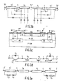
- Fig. 3a shows two coupled filter arrangements in accordance with the invention. Identical parts bear the same reference numerals as in Fig. 1, the parts of the second filter arrangement being primed.
- the input terminals 6 ⁇ and 7 ⁇ of the second filter arrangement are connected to the output terminals 5 and 4 of the first filter arrangement. It is to be noted that alternatively the inputs of the second filter arrangement may be cross-coupled to the outputs of the first filter arrangement.
- the amplifiers are constructed as shown in Fig. 2, regardless of how the entire filter arrangement is constructed, an input resistor and a load resistor are at any rate connected to each output. In fig. 3b these resistors are shown separately.
- the load resistors R5 and R4 of the first filter arrangement have large resistance values relative to the input resistors R1 ⁇ and R22 ⁇ of the second filter arrangement, so that substantially the entire output signal current flows through the resistors R1 ⁇ and R2 ⁇ .
- each of the resistors R1 ⁇ and R2 ⁇ is constructed as a diffused resistor and each of the resistors R4 and R5 is constructed as a buried resistor arranged in parallel therewith.
- the junction point between the resistors R4 and R5 constitutes a virtual signal-earth.
- the signal voltage on the non-inverting input 2 ⁇ and the inverting input 3 ⁇ is very small, so that these inputs may also be regarded as virtual signal-earths. Therefore, substantially the same signal voltage appears across the resistors R1 ⁇ and R5 and across the resistors R2 ⁇ and R4.
- Fig. 3c is a diagrammatic sectional view of the integrated circuit for the set of resistors R4 and R2 ⁇ .
- a P-SUB On a P-type substrate a P-SUB an N-type epitaxial layer N-EPI is deposited.
- N-EPI N-type epitaxial layer
- a P-type diffused or impplanted resistor SPB is formed with low-impedance end portions SP, constituting the resistor R2 ⁇ .
- an insulating layer ISO is arranged, in which metallised apertures MET1 and MET2 are formed at the location of the resistor end portions SP.
- One terminal MET1 is connected to the output 4 of the first filter arrangement and the other terminal MET 2 is connected to the input 2 ⁇ of the second filter arrangement.
- a partly buried layer BN is formed in the island beneath the resistor SPB .
- the high-impedance region N-EPI between the two portions of the buried layer BN constitutes the resistor R4.
- two metallised apertures MET3 and MET4 are formed, which are each connected to one terminal of the resistor R4 by means of a deep N-type diffusion DN and a portion of the buried layer BN.
- the terminal MET3 is connected to the output 4 of the first filter arrangement and the terminal MET 4 is connected to the junction point between the resistors R4 and R5.
- the filter arrangement can be fabricated completely by means of a bipolar process.
- the filter arrangement may be fabricated in a BIMOS or BICMOS process. These are processes in which both bipolar transistors and MOS transistors can be fabricated.
- the junction capacities are constructed as bipolar PN junctions, whilst the resistors may then be constructed as MOS transistors.
- MOS transistors also exhibit parasitic capacitances which adversely affect the behaviour of the filter arrangement. The channel-gate capacitance is the most important of these parasitic capacitances.
- This parasitic capacitance causes a MOS transistor to behave as a distributed RC-network in the same way as a diffused resistor, causing the signal to be phase-shifted.
- This phase shift can be compensated for by providing a compensation capacitor C p between the source and the drain of the transistor, as is shown in Fig. 3b. It is not necessary to arrange a compensation capacitor across the load resistors R4 and R5, because these resistors are not included in the signal path of the arrangement.
- the compensation capacitor has a value which is substantially equal to one sixth of the channel-gate capacitance.
- the MOS resistors may have fixed resistance values, but it is alternatively possible to make their resistance values adjustable by means of a control voltage applied to the gate of the MOS transistor.
- the RC-time constant of such a filter arrangement can then be adjusted to the desired value both by adjusting the capacitance values of the junction capacitors and by adjusting the resistance values of the MOS-resistors.
- the gates of the load resistors R4 and R5 are then connected to the gates of the resistors R1 ⁇ and R2 ⁇ .
- the parasitic capacitances between these resistors and the substrate can be compensated for by arranging a compensation capacitor C p across the resistor.
- This compensation capacitor C p provides first-order compensation.
- second-order compensation can be obtained by arranging a resistor R p in series with the capacitor C p .
- this resistor R p has a resistance value which is subsantially equal to 0.7 ⁇ the resistance value of the resistor to be compensated.
Landscapes
- Engineering & Computer Science (AREA)
- Power Engineering (AREA)
- Networks Using Active Elements (AREA)
- Amplifiers (AREA)
Applications Claiming Priority (2)
| Application Number | Priority Date | Filing Date | Title |
|---|---|---|---|
| NL8602893 | 1986-11-14 | ||
| NL8602893A NL8602893A (nl) | 1986-11-14 | 1986-11-14 | Filterschakeling. |
Publications (2)
| Publication Number | Publication Date |
|---|---|
| EP0269162A1 true EP0269162A1 (fr) | 1988-06-01 |
| EP0269162B1 EP0269162B1 (fr) | 1991-08-21 |
Family
ID=19848838
Family Applications (1)
| Application Number | Title | Priority Date | Filing Date |
|---|---|---|---|
| EP87202138A Expired - Lifetime EP0269162B1 (fr) | 1986-11-14 | 1987-11-05 | Dispositif de filtrage |
Country Status (8)
| Country | Link |
|---|---|
| US (1) | US4786880A (fr) |
| EP (1) | EP0269162B1 (fr) |
| JP (1) | JPH0714134B2 (fr) |
| KR (1) | KR960006643B1 (fr) |
| DE (1) | DE3772337D1 (fr) |
| HK (1) | HK76393A (fr) |
| NL (1) | NL8602893A (fr) |
| SG (1) | SG65693G (fr) |
Cited By (3)
| Publication number | Priority date | Publication date | Assignee | Title |
|---|---|---|---|---|
| EP0338316A3 (en) * | 1988-04-16 | 1990-08-29 | Telefunken Electronic Gmbh | Bandpass amplifier |
| EP0453680A3 (en) * | 1990-04-27 | 1991-11-27 | Precision Monolithics Inc. | Three-terminal operational amplifier and applications thereof |
| WO2003015262A1 (fr) * | 2001-07-31 | 2003-02-20 | Infineon Technologies Ag | Circuit de conversion tension/courant |
Families Citing this family (8)
| Publication number | Priority date | Publication date | Assignee | Title |
|---|---|---|---|---|
| EP0345880B1 (fr) * | 1988-06-08 | 1995-04-12 | Koninklijke Philips Electronics N.V. | Circuits de filtrage d'intégrateur symétriques |
| GB2225504A (en) * | 1988-11-18 | 1990-05-30 | Motorola Inc | Amplifier with compensation capacitance |
| US5883566A (en) * | 1997-02-24 | 1999-03-16 | International Business Machines Corporation | Noise-isolated buried resistor |
| JP2001062207A (ja) * | 1999-08-31 | 2001-03-13 | Asahi Tec Corp | 沈殿池用排泥装置 |
| WO2001069774A1 (fr) | 2000-03-14 | 2001-09-20 | Koninklijke Philips Electronics N.V. | Resonateur |
| KR20030048303A (ko) * | 2001-12-12 | 2003-06-19 | 주식회사 하빈 | 주위환경 자동적응형 디지털 오디오 재생장치 |
| US8362838B2 (en) * | 2007-01-19 | 2013-01-29 | Cirrus Logic, Inc. | Multi-stage amplifier with multiple sets of fixed and variable voltage rails |
| WO2015098057A1 (fr) | 2013-12-27 | 2015-07-02 | 株式会社ソシオネクスト | Intégrateur, modulateur sigma-delta et dispositif de communication |
Citations (4)
| Publication number | Priority date | Publication date | Assignee | Title |
|---|---|---|---|---|
| GB1142824A (en) * | 1967-06-21 | 1969-02-12 | Mullard Ltd | Amplifier circuits |
| GB1532060A (en) * | 1975-03-12 | 1978-11-15 | Sanyo Electric Co | Amplification circuits provided with automatic gain control means |
| DE3243145A1 (de) * | 1981-11-23 | 1983-06-01 | RCA Corp., 10020 New York, N.Y. | Differenzverstaerker |
| US4509019A (en) * | 1983-01-27 | 1985-04-02 | At&T Bell Laboratories | Tunable active filter |
-
1986
- 1986-11-14 NL NL8602893A patent/NL8602893A/nl not_active Application Discontinuation
-
1987
- 1987-03-31 US US07/033,140 patent/US4786880A/en not_active Expired - Lifetime
- 1987-11-05 DE DE8787202138T patent/DE3772337D1/de not_active Expired - Lifetime
- 1987-11-05 EP EP87202138A patent/EP0269162B1/fr not_active Expired - Lifetime
- 1987-11-06 JP JP62280851A patent/JPH0714134B2/ja not_active Expired - Lifetime
- 1987-11-13 KR KR87012781A patent/KR960006643B1/ko not_active Expired - Fee Related
-
1993
- 1993-05-20 SG SG65693A patent/SG65693G/en unknown
- 1993-07-29 HK HK763/93A patent/HK76393A/en not_active IP Right Cessation
Patent Citations (4)
| Publication number | Priority date | Publication date | Assignee | Title |
|---|---|---|---|---|
| GB1142824A (en) * | 1967-06-21 | 1969-02-12 | Mullard Ltd | Amplifier circuits |
| GB1532060A (en) * | 1975-03-12 | 1978-11-15 | Sanyo Electric Co | Amplification circuits provided with automatic gain control means |
| DE3243145A1 (de) * | 1981-11-23 | 1983-06-01 | RCA Corp., 10020 New York, N.Y. | Differenzverstaerker |
| US4509019A (en) * | 1983-01-27 | 1985-04-02 | At&T Bell Laboratories | Tunable active filter |
Cited By (3)
| Publication number | Priority date | Publication date | Assignee | Title |
|---|---|---|---|---|
| EP0338316A3 (en) * | 1988-04-16 | 1990-08-29 | Telefunken Electronic Gmbh | Bandpass amplifier |
| EP0453680A3 (en) * | 1990-04-27 | 1991-11-27 | Precision Monolithics Inc. | Three-terminal operational amplifier and applications thereof |
| WO2003015262A1 (fr) * | 2001-07-31 | 2003-02-20 | Infineon Technologies Ag | Circuit de conversion tension/courant |
Also Published As
| Publication number | Publication date |
|---|---|
| JPS63136707A (ja) | 1988-06-08 |
| DE3772337D1 (de) | 1991-09-26 |
| JPH0714134B2 (ja) | 1995-02-15 |
| SG65693G (en) | 1993-08-06 |
| HK76393A (en) | 1993-08-06 |
| KR960006643B1 (en) | 1996-05-22 |
| KR880006842A (ko) | 1988-07-25 |
| NL8602893A (nl) | 1988-06-01 |
| EP0269162B1 (fr) | 1991-08-21 |
| US4786880A (en) | 1988-11-22 |
Similar Documents
| Publication | Publication Date | Title |
|---|---|---|
| JP2766264B2 (ja) | 差動増幅回路 | |
| JP5377676B2 (ja) | 高直線性デジタル可変利得増幅器 | |
| US6864751B1 (en) | Transimpedance amplifier with adjustable output amplitude and wide input dynamic-range | |
| US5942929A (en) | Active phase splitter | |
| EP0269162B1 (fr) | Dispositif de filtrage | |
| US5900779A (en) | Differential transimpedance amplifier | |
| US7626458B2 (en) | Common-mode bandwidth reduction circuit and method for differential applications | |
| US5945880A (en) | Low noise amplifier | |
| US5939944A (en) | NPN push-pull output stage with folded cascode JFETs | |
| US5495201A (en) | Transconductor stage | |
| US20050093628A1 (en) | Differential amplifier circuit and multistage amplifier circuit | |
| US4918402A (en) | Delay circuit having at least one all-pass network | |
| US5166560A (en) | Voltage-controlled variable capacitor | |
| US6031424A (en) | Differential amplifier with improved voltage gain using operational amplifiers to eliminate diode voltage drops | |
| US5475338A (en) | Active filter circuit of a capacity ground type | |
| US5859566A (en) | Electronic circuit comprising complementary transconductors for filters and oscillators | |
| US5760642A (en) | Filter circuit using a junction capacitor of a semiconductor | |
| WO1990012454A1 (fr) | Circuits gyrateurs | |
| JP2001298324A (ja) | 発振回路 | |
| US5694071A (en) | Electronic device comprising means for compensating an undesired capacitance | |
| US4937534A (en) | Band-pass amplifier | |
| JPH04369113A (ja) | 主信号通路とハイパスフィルター特性の補助的な信号通路を有するノイズ減衰回路 | |
| US20220149790A1 (en) | Variable gain amplifier circuit and semiconductor integrated circuit | |
| JPH07336171A (ja) | 可変利得増幅回路 | |
| HK1000270B (en) | Bandpass amplifier |
Legal Events
| Date | Code | Title | Description |
|---|---|---|---|
| PUAI | Public reference made under article 153(3) epc to a published international application that has entered the european phase |
Free format text: ORIGINAL CODE: 0009012 |
|
| AK | Designated contracting states |
Kind code of ref document: A1 Designated state(s): DE FR GB IT NL SE |
|
| 17P | Request for examination filed |
Effective date: 19881128 |
|
| 17Q | First examination report despatched |
Effective date: 19901010 |
|
| GRAA | (expected) grant |
Free format text: ORIGINAL CODE: 0009210 |
|
| AK | Designated contracting states |
Kind code of ref document: B1 Designated state(s): DE FR GB IT NL SE |
|
| PG25 | Lapsed in a contracting state [announced via postgrant information from national office to epo] |
Ref country code: NL Effective date: 19910821 |
|
| REF | Corresponds to: |
Ref document number: 3772337 Country of ref document: DE Date of ref document: 19910926 |
|
| ITF | It: translation for a ep patent filed | ||
| ET | Fr: translation filed | ||
| NLV1 | Nl: lapsed or annulled due to failure to fulfill the requirements of art. 29p and 29m of the patents act | ||
| PLBE | No opposition filed within time limit |
Free format text: ORIGINAL CODE: 0009261 |
|
| STAA | Information on the status of an ep patent application or granted ep patent |
Free format text: STATUS: NO OPPOSITION FILED WITHIN TIME LIMIT |
|
| 26N | No opposition filed | ||
| EAL | Se: european patent in force in sweden |
Ref document number: 87202138.1 |
|
| ITPR | It: changes in ownership of a european patent |
Owner name: CAMBIO RAGIONE SOCIALE;PHILIPS ELECTRONICS N.V. |
|
| REG | Reference to a national code |
Ref country code: FR Ref legal event code: CD |
|
| PGFP | Annual fee paid to national office [announced via postgrant information from national office to epo] |
Ref country code: GB Payment date: 19961101 Year of fee payment: 10 |
|
| PGFP | Annual fee paid to national office [announced via postgrant information from national office to epo] |
Ref country code: FR Payment date: 19961119 Year of fee payment: 10 |
|
| PGFP | Annual fee paid to national office [announced via postgrant information from national office to epo] |
Ref country code: SE Payment date: 19961126 Year of fee payment: 10 |
|
| PG25 | Lapsed in a contracting state [announced via postgrant information from national office to epo] |
Ref country code: GB Free format text: LAPSE BECAUSE OF NON-PAYMENT OF DUE FEES Effective date: 19971105 |
|
| PG25 | Lapsed in a contracting state [announced via postgrant information from national office to epo] |
Ref country code: SE Free format text: LAPSE BECAUSE OF NON-PAYMENT OF DUE FEES Effective date: 19971106 |
|
| PG25 | Lapsed in a contracting state [announced via postgrant information from national office to epo] |
Ref country code: FR Free format text: THE PATENT HAS BEEN ANNULLED BY A DECISION OF A NATIONAL AUTHORITY Effective date: 19971130 |
|
| GBPC | Gb: european patent ceased through non-payment of renewal fee |
Effective date: 19971105 |
|
| EUG | Se: european patent has lapsed |
Ref document number: 87202138.1 |
|
| REG | Reference to a national code |
Ref country code: FR Ref legal event code: ST |
|
| PGFP | Annual fee paid to national office [announced via postgrant information from national office to epo] |
Ref country code: DE Payment date: 20000119 Year of fee payment: 13 |
|
| PG25 | Lapsed in a contracting state [announced via postgrant information from national office to epo] |
Ref country code: DE Free format text: LAPSE BECAUSE OF NON-PAYMENT OF DUE FEES Effective date: 20010801 |
|
| PG25 | Lapsed in a contracting state [announced via postgrant information from national office to epo] |
Ref country code: IT Free format text: LAPSE BECAUSE OF NON-PAYMENT OF DUE FEES Effective date: 20051105 |