EP0269475A1 - Schutz einer elektropyrotechnischen Vorrichtung gegen elektrostatische Entladungen - Google Patents
Schutz einer elektropyrotechnischen Vorrichtung gegen elektrostatische Entladungen Download PDFInfo
- Publication number
- EP0269475A1 EP0269475A1 EP87402337A EP87402337A EP0269475A1 EP 0269475 A1 EP0269475 A1 EP 0269475A1 EP 87402337 A EP87402337 A EP 87402337A EP 87402337 A EP87402337 A EP 87402337A EP 0269475 A1 EP0269475 A1 EP 0269475A1
- Authority
- EP
- European Patent Office
- Prior art keywords
- conductive
- spark gap
- substrate
- layer
- insulating
- Prior art date
- Legal status (The legal status is an assumption and is not a legal conclusion. Google has not performed a legal analysis and makes no representation as to the accuracy of the status listed.)
- Granted
Links
- 230000004224 protection Effects 0.000 title claims abstract description 27
- 230000015556 catabolic process Effects 0.000 claims abstract description 34
- 239000000758 substrate Substances 0.000 claims abstract description 30
- 239000000203 mixture Substances 0.000 claims abstract description 20
- 230000008021 deposition Effects 0.000 claims abstract description 7
- 239000011810 insulating material Substances 0.000 claims abstract description 7
- 230000000694 effects Effects 0.000 claims abstract description 5
- 239000010410 layer Substances 0.000 claims description 70
- 238000000151 deposition Methods 0.000 claims description 15
- 239000004020 conductor Substances 0.000 claims description 5
- 230000001681 protective effect Effects 0.000 claims description 3
- 239000002344 surface layer Substances 0.000 claims description 2
- 230000000977 initiatory effect Effects 0.000 description 6
- 238000004519 manufacturing process Methods 0.000 description 5
- 238000000034 method Methods 0.000 description 5
- 239000011248 coating agent Substances 0.000 description 4
- 238000000576 coating method Methods 0.000 description 4
- 230000015572 biosynthetic process Effects 0.000 description 3
- 238000003466 welding Methods 0.000 description 3
- VYPSYNLAJGMNEJ-UHFFFAOYSA-N Silicium dioxide Chemical compound O=[Si]=O VYPSYNLAJGMNEJ-UHFFFAOYSA-N 0.000 description 2
- 238000005137 deposition process Methods 0.000 description 2
- 229920001971 elastomer Polymers 0.000 description 2
- 239000000806 elastomer Substances 0.000 description 2
- 238000005530 etching Methods 0.000 description 2
- 230000008020 evaporation Effects 0.000 description 2
- 238000001704 evaporation Methods 0.000 description 2
- 238000010849 ion bombardment Methods 0.000 description 2
- 230000000873 masking effect Effects 0.000 description 2
- 239000002184 metal Substances 0.000 description 2
- 238000001465 metallisation Methods 0.000 description 2
- 239000004065 semiconductor Substances 0.000 description 2
- 239000000126 substance Substances 0.000 description 2
- 230000016571 aggressive behavior Effects 0.000 description 1
- 238000005234 chemical deposition Methods 0.000 description 1
- 238000013461 design Methods 0.000 description 1
- 238000005474 detonation Methods 0.000 description 1
- 238000005516 engineering process Methods 0.000 description 1
- 230000010006 flight Effects 0.000 description 1
- 230000017525 heat dissipation Effects 0.000 description 1
- 238000010348 incorporation Methods 0.000 description 1
- 230000010354 integration Effects 0.000 description 1
- 238000002955 isolation Methods 0.000 description 1
- 238000003754 machining Methods 0.000 description 1
- 238000012423 maintenance Methods 0.000 description 1
- 239000000463 material Substances 0.000 description 1
- 238000012986 modification Methods 0.000 description 1
- 230000004048 modification Effects 0.000 description 1
- 239000002245 particle Substances 0.000 description 1
- 238000007789 sealing Methods 0.000 description 1
- 235000012239 silicon dioxide Nutrition 0.000 description 1
- 239000000377 silicon dioxide Substances 0.000 description 1
- 238000005507 spraying Methods 0.000 description 1
- 238000004544 sputter deposition Methods 0.000 description 1
- 229920001169 thermoplastic Polymers 0.000 description 1
- 239000004416 thermosoftening plastic Substances 0.000 description 1
Images


Classifications
-
- F—MECHANICAL ENGINEERING; LIGHTING; HEATING; WEAPONS; BLASTING
- F42—AMMUNITION; BLASTING
- F42B—EXPLOSIVE CHARGES, e.g. FOR BLASTING, FIREWORKS, AMMUNITION
- F42B3/00—Blasting cartridges, i.e. case and explosive
- F42B3/10—Initiators therefor
- F42B3/18—Safety initiators resistant to premature firing by static electricity or stray currents
Definitions
- the present invention relates to the protection of electro-pyrotechnic devices against electrostatic discharges.
- the ignition of the pyrotechnic composition is produced by the heat given off by the Joule effect by an initiation circuit comprising at least one resistant element placed in contact with the pyrotechnic composition and supplied with electric current by connection pins.
- the invention more particularly relates to the protection of electro-pyrotechnic devices with respect to electrostatic discharges between isolated points.
- the object of the present invention is to provide a means of protection which can be easily integrated into electro-pyrotechnic devices and allows, at a relatively low cost, to obtain a constant and invariable breakdown voltage.
- spark gap protection device providing a breakdown zone at least between each connection pin and the ground
- protection device in which, according to the invention, the spark gap comprises a substrate of which at least the surface layer is conductive and is connected to ground, an insulating layer in one or more parts formed on the substrate by depositing a thin layer of insulating material, and conductive layers connected respectively to the connection pins and formed in different zones on the insulating layer to arrange said breakdown zones through the insulating layer between the substrate and, respectively, each of the conductive layers.
- An important characteristic of the invention consists in the production of the insulating layer by a deposition process.
- Any known deposition process can be used, in particular the processes for forming thin or thick layers in the field of manufacturing semiconductors and integrated circuits.
- the insulating layer may be produced by evaporation, spraying, ion bombardment, chemical or other deposition.
- the delimitation of the insulating layer or its possible machining are likewise carried out by any known method, for example by masking or by chemical or ionic etching.
- the formation of the insulating layer by deposition in a thin layer provides several advantages.
- the breakdown voltage is easily adjustable on demand by adjusting the thickness of the deposit of the insulating layer.
- spark gap is easily adaptable to all electro-pyrotechnic devices regardless of the arrangements and the number of isolated points to be protected.
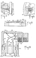
- FIG. 1 shows an electro-pyrotechnic device which, in a manner known per se, comprises a resistant element 10 in contact with a pyrotechnic composition 12 housed in a cylindrical envelope 14.
- Connection pins 16, 18 allow the electrical supply of the resistive element 10 for causing the pyrotechnic composition to ignite by the heat released by the Joule effect.
- connection pins 16, 18 pass through an insulating piece 20 to which they are sealed.
- the pins 16, 18 are connected to the resistant element 10 on the side of the insulating piece 20 in contact with the pyrotechnic composition 12 and protrude from the opposite side of the piece 20 to be connected to a socket (not shown) allowing connection with a source of electrical energy.
- the pyrotechnic composition 12 is housed in the cylindrical body 22 of the electro-pyrotechnic device by means of an antistatic skirt 24 which supports the casing 14 and which is itself held inside the body 22.
- the maintenance of the insulating part 20 is provided by a centering ring 26 also housed in the body 22.
- the rest of the electro-pyrotechnic device, in particular the lower part of the body 22 which may contain specific ignition or detonation compositions, is not shown .
- the protection of the device described above against electrostatic discharges between isolated points is provided by a thin layer spark gap.
- the spark gap 30 comprises a conductive metallic substrate 32 which is placed on the insulating piece 20 on the side thereof opposite the pyrotechnic composition 10.
- the substrate 32 is of annular shape and is carried by an internal shoulder 28 of the body 22 to which it is fixed, for example by welding, which ensures the connection of the substrate 32 to the mechanical and electrical mass of the electro-pyrotechnic device.
- the body 22 is formed in several parts: an upper part carrying the spark gap, an intermediate part carrying the skirt 24 and the ring 26 and a lower part containing the rest of the device, these different parts being assembled end to end by welding.
- the annular substrate 32 is crossed by the pins 16, 18 and sufficient clearance is provided between the pins 16, 18 and the wall of the central passage of the substrate 32 so that the intervals between these parts cannot constitute preferential arc paths. electrostatic discharge.
- these preferential paths consist of breakdown zones 40, 42 arranged on the substrate 32 to provide protection against electrostatic attacks between the ground and, respectively, the pins 16, 18.
- Each breakdown zone is located within an insulating layer formed by a thin layer deposition of an insulating material on the conductive substrate 32.
- the insulating layer may be in a single part common to the two breakdown zones or, as in the example illustrated, in two parts 44, 46 formed in different zones of the surface of the substrate 32 (see in particular FIG. 3).
- Conductive layers, or electrodes 48, 50 are formed on the insulating layer or layers 44, 46 also by depositing a thin layer of a conductive material.
- the electrical connections between the electrodes 48, 50 and, respectively, the pins 16, 18 are provided by conductive filaments 52, 54 welded at one end to the electrodes 48, 50, respectively, and at the other end on elastic conductive rings 56, 58 enclosing the pins 16, 18, respectively.
- the insulating layers 44, 46 are deposited by any known method of deposition in a thin or thick layer used in the technology for manufacturing semiconductors and integrated circuits, for example by evaporation, sputtering, ion bombardment or chemical deposition. Likewise, the design of the insulating layer or layers is obtained by any known method of masking or etching. The formation of the conductive layers 48, 50 on the insulating layers 44, 46 is also carried out by any known method of depositing thin or thick conductive layers.
- the production of the insulating layer or layers 44, 46 by a thin layer deposition technique makes it possible to precisely adjust the breakdown voltage by adjusting the thickness of the deposited insulating layer.
- layers of silicon dioxide with a thickness equal to 2.5 microns made it possible to obtain breakdown voltages of approximately 800 V.
- the protection device according to the invention has other advantages. It is first of all quite apparent that its integration into the electro-pyrotechnic device is easy to carry out. In addition, not only can a precise breakdown voltage be obtained, but this breakdown voltage retains its value after several series of electrostatic discharges and despite modifications to the environment of the device (in particular pressure and nature of the surrounding medium).
- the breakdown zones can be formed on any face of the substrate 32.
- an insulating substrate for example the insulating part 20 itself, on which a connected conductive metallic layer is deposited. to the mechanical and electrical mass of the electro-pyrotechnic device.
- the insulating layer (s) and the conductive electrodes defining the breakdown zones are then formed on this surface metal layer.
- FIG. 4 Another alternative embodiment of the spark gap is illustrated by Figures 4 and 5.
- the elements common with the device of Figures 1 to 3 have the same references.
- each breakdown zone is arranged on the face of the substrate 32 facing the insulating part 20.
- Each breakdown zone for example 40 ⁇ , is formed by a thin insulating layer 44 ⁇ deposited on the conductive substrate 32 and a conductive layer or 48 ⁇ electrode deposited on layer 44 ⁇ .
- the electrical connection between the electrode 48 ⁇ and the pin 16 is produced by a metallic coating 52 ⁇ deposited on the insulating part 20 and forming a conductive path between the zone of the part 20 which comes into contact with the electrode 46 ⁇ and a metallization 56 'of the hole 16 formed in the insulating part 20 for the passage of the spindle 16.
- 52' coating may be formed in a recess of the insulating part 20. the surface 52' coating is polished at the same time as that of the part 20 so as to be in the same plane and not have any roughness liable to damage the insulating layer 44 ⁇ .
- the electrical contact between the pin 16 and the metallization 56 ⁇ is ensured by the sealing of the pin in the hole 16a.
- the electrical contact between the electrode 48 ⁇ and the coating 52 ⁇ is ensured by the pressure exerted on mounting the device between the skirt 24, which is supported by its lower edge on the underside of the envelope 14 of the pyrotechnic composition 12, and the shoulder 28 which rests on the upper face of the substrate 32.
- the permanence of this pressure contact can be ensured by elastic means, for example an elastomer layer 28 a interposed between the shoulder 28 and the substrate 32.
- electro-pyrotechnic device comprising a single resistant element.
- the invention is likewise applicable to electro-pyrotechnic devices comprising, for reasons of redundancy, two resistive elements aunts. Such a device with two resistant elements is illustrated in FIGS. 6 and 8.
- each resistant element 110, 111 is located in contact with a pyrotechnic composition 112 housed in a cylindrical envelope 114.
- Connection pins 116, 118 are provided for the electrical supply of the resistive element 110, as well as pins 117, 119 for supplying the resistive element 111.
- the electrical energy is supplied by means of a connector 101 fixed laterally to the upper part of the body 122 of the electro-pyrotechnic device.
- the circuits 116-110-118 and 117-111-119 are connected in parallel on the terminals 102 and 103 on connector 101, the connections between the pins 116 to 119 and the terminals 102, 103 being produced by flexible conductors 104 to 107
- the pins 116 to 119 pass through an insulating part 120 to which they are sealed and which is placed in contact with the pyrotechnic composition 112. Maintaining this composition 112 and the insulating part 120 in the body 122 of the electro-pyrotechnic device is provided by means of an antistatic skirt 124 and a ring 126, as in the embodiment of FIG. 1.
- the protection of the device described above against electrostatic discharges is ensured by means of a thin layer spark gap.
- the spark gap 130 provides six breakdown zones between the connection pins and the mass of the device, as well as between connection pins connected to different resistant elements. It should be noted that three breakdown zones could be sufficient due to the parallel connection of the connection pins. The choice of six different breakdown zones is dictated here for the sake of redundancy.
- the spark gap 130 shown in FIGS. 6 to 8 comprises a metallic annular substrate 132 placed on the insulating part 120 and crossed by the pins 116 to 119.
- the conductive substrate 132 is fixed by welding to an internal shoulder 128 of the body 122, this which ensures its connection to the mechanical and electrical ground of the device.
- Breakdown zones 140, 141, 142, 143 between the mass and, respectively, the pins 116, 117, 118 and 119 are formed on the substrate 132.
- the latter is coated with an insulating layer 144 formed by a thin layer deposition of an insulating material.
- Conductive layers or electrodes 148, 149, 150, 151 are formed by depositing a thin layer of a conductive material on the insulating layer 144 in different zones distributed around the periphery of the spark gap (see in particular FIG. 8).
- Conductive filaments 152, 153, 154, 155 connect the electrodes 148 to 151 respectively to elastic conductive rings 156, 157, 158, 159 enclosing the pins 116 to 119.
- the insulating layer 144 may be formed in several separate parts each carrying a particular electrode.
- Two additional breakdown zones 240 and 242 are formed on the spark gap 130 for the protection of electrostatic attacks respectively between the connection pins 116 and 117 and between the connection pins 118 and 119, that is to say between connected pins to different resistant elements.
- the breakdown zones 240, 242 are arranged by forming insulating layers 244, 246 by depositing a thin layer of insulating material on the electrodes 148, 150 connected to the pins 116, 118.
- Conductive layers, or electrodes, 249, 251 are formed on the insulating layers 244, 246 by depositing a thin layer of a conductive material.
- the electrodes 249, 251 are electrically connected to the pins 117, 119.
- Another solution consists, as in the example illustrated, in extending the conductive layers 249, 251 until at least partially covering the electrodes 149, 151.
- the conductive filaments 153 and 155 which make the connection with the pins 118 and 120 can then be welded on the electrodes 249, 251.
- the additional breakdown zones between connection pins can be formed on the electrodes 149, 151 instead of being formed on the electrodes 148, 150.
- FIG. 9 finally illustrates another assembly of a protection device according to the invention for an electro-pyrotechnic device with two insulating elements.
- the device of FIG. 9 differs from that of FIGS. 6 to 8 essentially in that the spark gap 130 ⁇ constitutes a cover closing the body 122 at its upper end.
- the metallic substrate 132 ⁇ is connected to the mechanical and electrical ground, for example by screwing onto the body 122, while the breakdown zones are arranged on the underside of the substrate 132 ⁇ .
- the spark gap is identical to that described with reference to FIGS. 6 to 8.
- spark gap in the electro-pyrotechnic device could be adopted insofar as they contribute to providing breakdown zones remote from the pyrotechnic composition.
Landscapes
- Engineering & Computer Science (AREA)
- General Engineering & Computer Science (AREA)
- Air Bags (AREA)
Applications Claiming Priority (2)
| Application Number | Priority Date | Filing Date | Title |
|---|---|---|---|
| FR8614923 | 1986-10-27 | ||
| FR8614923A FR2605827B1 (fr) | 1986-10-27 | 1986-10-27 | Protection d'un dispositif electro-pyrotechnique vis-a-vis des decharges electrostatiques |
Publications (2)
| Publication Number | Publication Date |
|---|---|
| EP0269475A1 true EP0269475A1 (de) | 1988-06-01 |
| EP0269475B1 EP0269475B1 (de) | 1991-03-27 |
Family
ID=9340233
Family Applications (1)
| Application Number | Title | Priority Date | Filing Date |
|---|---|---|---|
| EP19870402337 Expired - Lifetime EP0269475B1 (de) | 1986-10-27 | 1987-10-20 | Schutz einer elektropyrotechnischen Vorrichtung gegen elektrostatische Entladungen |
Country Status (3)
| Country | Link |
|---|---|
| EP (1) | EP0269475B1 (de) |
| DE (1) | DE3768918D1 (de) |
| FR (1) | FR2605827B1 (de) |
Cited By (4)
| Publication number | Priority date | Publication date | Assignee | Title |
|---|---|---|---|---|
| GB2281608A (en) * | 1993-08-25 | 1995-03-08 | Ems Patvag Ag | Igniting device for a gas generator |
| US5639986A (en) * | 1993-11-18 | 1997-06-17 | Ici Americas Inc. | Airbag igniter and method of manufacture |
| WO1999036293A1 (de) * | 1998-01-19 | 1999-07-22 | Autoliv Development Ab | Zündvorrichtung für einen gasgenerator |
| US6601514B1 (en) * | 1998-08-11 | 2003-08-05 | Dynamit Nobel Gmbh Explosivstoff-Und Systemtechnik | Externally controlled ignition unit with integrated electronic system for triggering a restraint system |
Citations (4)
| Publication number | Priority date | Publication date | Assignee | Title |
|---|---|---|---|---|
| US3333538A (en) * | 1966-06-09 | 1967-08-01 | Hercules Inc | Electric initiator structure |
| US4061088A (en) * | 1975-11-13 | 1977-12-06 | Toyota Jidosha Kogyo Kabushiki Kaisha | Electric detonating fuse assembly |
| EP0029671A1 (de) * | 1979-11-20 | 1981-06-03 | Ici Americas Inc. | Elektrostatisches Sicherheitselement für einen elektrischen Initialzünder |
| DE3415625A1 (de) * | 1984-04-26 | 1985-10-31 | Dynamit Nobel Ag, 5210 Troisdorf | Elektrisches zuendelement mit soll-funkenstrecke |
-
1986
- 1986-10-27 FR FR8614923A patent/FR2605827B1/fr not_active Expired
-
1987
- 1987-10-20 DE DE8787402337T patent/DE3768918D1/de not_active Expired - Lifetime
- 1987-10-20 EP EP19870402337 patent/EP0269475B1/de not_active Expired - Lifetime
Patent Citations (4)
| Publication number | Priority date | Publication date | Assignee | Title |
|---|---|---|---|---|
| US3333538A (en) * | 1966-06-09 | 1967-08-01 | Hercules Inc | Electric initiator structure |
| US4061088A (en) * | 1975-11-13 | 1977-12-06 | Toyota Jidosha Kogyo Kabushiki Kaisha | Electric detonating fuse assembly |
| EP0029671A1 (de) * | 1979-11-20 | 1981-06-03 | Ici Americas Inc. | Elektrostatisches Sicherheitselement für einen elektrischen Initialzünder |
| DE3415625A1 (de) * | 1984-04-26 | 1985-10-31 | Dynamit Nobel Ag, 5210 Troisdorf | Elektrisches zuendelement mit soll-funkenstrecke |
Cited By (5)
| Publication number | Priority date | Publication date | Assignee | Title |
|---|---|---|---|---|
| GB2281608A (en) * | 1993-08-25 | 1995-03-08 | Ems Patvag Ag | Igniting device for a gas generator |
| US5596163A (en) * | 1993-08-25 | 1997-01-21 | Ems-Patvag Ag | Gas generator igniting capsule |
| US5639986A (en) * | 1993-11-18 | 1997-06-17 | Ici Americas Inc. | Airbag igniter and method of manufacture |
| WO1999036293A1 (de) * | 1998-01-19 | 1999-07-22 | Autoliv Development Ab | Zündvorrichtung für einen gasgenerator |
| US6601514B1 (en) * | 1998-08-11 | 2003-08-05 | Dynamit Nobel Gmbh Explosivstoff-Und Systemtechnik | Externally controlled ignition unit with integrated electronic system for triggering a restraint system |
Also Published As
| Publication number | Publication date |
|---|---|
| FR2605827A1 (fr) | 1988-04-29 |
| FR2605827B1 (fr) | 1989-07-07 |
| DE3768918D1 (de) | 1991-05-02 |
| EP0269475B1 (de) | 1991-03-27 |
Similar Documents
| Publication | Publication Date | Title |
|---|---|---|
| EP0228953B1 (de) | Verkapselungsgehäuse für eine elektronische Schaltung | |
| EP0133125B1 (de) | Gehäuse für einen elektronischen Baustein mit einem Kondensator | |
| EP0497948B1 (de) | Verfahren und vorrichtung zur hermetischen verkapselung von elektronischen bauteilen | |
| EP3319194B1 (de) | Schutzvorrichtung gegen vorübergehende überspannungen | |
| EP0318339B1 (de) | Funkenstrecken-Überspannungsableiter mit wenigstens einem Schmelzleiter | |
| CA2056170A1 (fr) | Detonateur pyrotechnique a connexions coaxiales | |
| FR2527039A1 (fr) | Dispositif de protection d'un dispositif electronique contre les tensions engendrees par un champ electromagnetique | |
| FR2700416A1 (fr) | Dispositif à semiconducteurs comportant un élément semiconducteur sur un élément de montage. | |
| EP0673068B1 (de) | Schutzeinrichtung gegen Überspannungen in integrierten Schaltungen | |
| EP0600810B1 (de) | Überspannungsschutzeinrichtung | |
| EP3712908A1 (de) | Schutzvorrichtung gegen überspannungen | |
| EP0269475B1 (de) | Schutz einer elektropyrotechnischen Vorrichtung gegen elektrostatische Entladungen | |
| FR2513032A1 (fr) | Dispositif de protection integre contre les surtensions d'un circuit electronique, et circuit electronique protege par ce dispositif | |
| EP3226303B1 (de) | Leistungskomponente mit überhitzungsschutz | |
| WO1987006768A1 (fr) | Composant semiconducteur de protection contre les surtensions et surintensites | |
| EP0166634A1 (de) | Einrichtung zur Verteilung von elektrischen Potentialen, und eine solche Einrichtung enthaltendes Gehäuse für elektronische Komponenten | |
| FR2555801A1 (fr) | Condensateur de decouplage pour circuits integres et sous-assemblage electronique comprenant un tel condensateur | |
| EP3942577B1 (de) | Überspannungsschutz | |
| FR2668847A1 (fr) | Methode de protection de composants electroniques d'un circuit contre les radiations et dispositif utilisant cette methode. | |
| EP0554195B1 (de) | Selbsttätig geschütztes Halbleiterschutzelement | |
| EP0191255B1 (de) | Integrierte Anordnung eines durch einen Diac gesteuerten Triac | |
| FR2879348A1 (fr) | Protection d'un condensateur integre | |
| FR2726941A1 (fr) | Dispositif integre de protection par varistance d'un composant electronique contre les effets d'un champ electro-magnetique ou de charges statiques | |
| EP0112254B1 (de) | Elektrischer Brückenzünder | |
| EP0545748B1 (de) | Anordnung zur Zuführung einer Spannung auf einen Substrathalter |
Legal Events
| Date | Code | Title | Description |
|---|---|---|---|
| PUAI | Public reference made under article 153(3) epc to a published international application that has entered the european phase |
Free format text: ORIGINAL CODE: 0009012 |
|
| AK | Designated contracting states |
Kind code of ref document: A1 Designated state(s): DE GB IT |
|
| 17P | Request for examination filed |
Effective date: 19881123 |
|
| 17Q | First examination report despatched |
Effective date: 19890719 |
|
| ITF | It: translation for a ep patent filed | ||
| GRAA | (expected) grant |
Free format text: ORIGINAL CODE: 0009210 |
|
| AK | Designated contracting states |
Kind code of ref document: B1 Designated state(s): DE GB IT |
|
| GBT | Gb: translation of ep patent filed (gb section 77(6)(a)/1977) | ||
| REF | Corresponds to: |
Ref document number: 3768918 Country of ref document: DE Date of ref document: 19910502 |
|
| PLBE | No opposition filed within time limit |
Free format text: ORIGINAL CODE: 0009261 |
|
| STAA | Information on the status of an ep patent application or granted ep patent |
Free format text: STATUS: NO OPPOSITION FILED WITHIN TIME LIMIT |
|
| 26N | No opposition filed | ||
| REG | Reference to a national code |
Ref country code: GB Ref legal event code: 732E |
|
| REG | Reference to a national code |
Ref country code: GB Ref legal event code: IF02 |
|
| PGFP | Annual fee paid to national office [announced via postgrant information from national office to epo] |
Ref country code: DE Payment date: 20021007 Year of fee payment: 16 |
|
| PGFP | Annual fee paid to national office [announced via postgrant information from national office to epo] |
Ref country code: GB Payment date: 20021015 Year of fee payment: 16 |
|
| PG25 | Lapsed in a contracting state [announced via postgrant information from national office to epo] |
Ref country code: GB Free format text: LAPSE BECAUSE OF NON-PAYMENT OF DUE FEES Effective date: 20031020 |
|
| PG25 | Lapsed in a contracting state [announced via postgrant information from national office to epo] |
Ref country code: DE Free format text: LAPSE BECAUSE OF NON-PAYMENT OF DUE FEES Effective date: 20040501 |
|
| GBPC | Gb: european patent ceased through non-payment of renewal fee |
Effective date: 20031020 |
|
| PG25 | Lapsed in a contracting state [announced via postgrant information from national office to epo] |
Ref country code: IT Free format text: LAPSE BECAUSE OF NON-PAYMENT OF DUE FEES;WARNING: LAPSES OF ITALIAN PATENTS WITH EFFECTIVE DATE BEFORE 2007 MAY HAVE OCCURRED AT ANY TIME BEFORE 2007. THE CORRECT EFFECTIVE DATE MAY BE DIFFERENT FROM THE ONE RECORDED. Effective date: 20051020 |