EP0166634A1 - Einrichtung zur Verteilung von elektrischen Potentialen, und eine solche Einrichtung enthaltendes Gehäuse für elektronische Komponenten - Google Patents
Einrichtung zur Verteilung von elektrischen Potentialen, und eine solche Einrichtung enthaltendes Gehäuse für elektronische Komponenten Download PDFInfo
- Publication number
- EP0166634A1 EP0166634A1 EP85400992A EP85400992A EP0166634A1 EP 0166634 A1 EP0166634 A1 EP 0166634A1 EP 85400992 A EP85400992 A EP 85400992A EP 85400992 A EP85400992 A EP 85400992A EP 0166634 A1 EP0166634 A1 EP 0166634A1
- Authority
- EP
- European Patent Office
- Prior art keywords
- component
- housing
- base
- potentials
- connection
- Prior art date
- Legal status (The legal status is an assumption and is not a legal conclusion. Google has not performed a legal analysis and makes no representation as to the accuracy of the status listed.)
- Granted
Links
Images


Classifications
-
- H—ELECTRICITY
- H10—SEMICONDUCTOR DEVICES; ELECTRIC SOLID-STATE DEVICES NOT OTHERWISE PROVIDED FOR
- H10W—GENERIC PACKAGES, INTERCONNECTIONS, CONNECTORS OR OTHER CONSTRUCTIONAL DETAILS OF DEVICES COVERED BY CLASS H10
- H10W76/00—Containers; Fillings or auxiliary members therefor; Seals
- H10W76/10—Containers or parts thereof
- H10W76/12—Containers or parts thereof characterised by their shape
- H10W76/15—Containers comprising an insulating or insulated base
- H10W76/157—Containers comprising an insulating or insulated base having interconnections parallel to the insulating or insulated base
-
- H—ELECTRICITY
- H10—SEMICONDUCTOR DEVICES; ELECTRIC SOLID-STATE DEVICES NOT OTHERWISE PROVIDED FOR
- H10W—GENERIC PACKAGES, INTERCONNECTIONS, CONNECTORS OR OTHER CONSTRUCTIONAL DETAILS OF DEVICES COVERED BY CLASS H10
- H10W44/00—Electrical arrangements for controlling or matching impedance
- H10W44/601—Capacitive arrangements
-
- H—ELECTRICITY
- H10—SEMICONDUCTOR DEVICES; ELECTRIC SOLID-STATE DEVICES NOT OTHERWISE PROVIDED FOR
- H10W—GENERIC PACKAGES, INTERCONNECTIONS, CONNECTORS OR OTHER CONSTRUCTIONAL DETAILS OF DEVICES COVERED BY CLASS H10
- H10W70/00—Package substrates; Interposers; Redistribution layers [RDL]
- H10W70/60—Insulating or insulated package substrates; Interposers; Redistribution layers
- H10W70/62—Insulating or insulated package substrates; Interposers; Redistribution layers characterised by their interconnections
- H10W70/63—Vias, e.g. via plugs
- H10W70/635—Through-vias
-
- H—ELECTRICITY
- H10—SEMICONDUCTOR DEVICES; ELECTRIC SOLID-STATE DEVICES NOT OTHERWISE PROVIDED FOR
- H10W—GENERIC PACKAGES, INTERCONNECTIONS, CONNECTORS OR OTHER CONSTRUCTIONAL DETAILS OF DEVICES COVERED BY CLASS H10
- H10W70/00—Package substrates; Interposers; Redistribution layers [RDL]
- H10W70/60—Insulating or insulated package substrates; Interposers; Redistribution layers
- H10W70/67—Insulating or insulated package substrates; Interposers; Redistribution layers characterised by their insulating layers or insulating parts
- H10W70/68—Shapes or dispositions thereof
- H10W70/682—Shapes or dispositions thereof comprising holes having chips therein
-
- H—ELECTRICITY
- H10—SEMICONDUCTOR DEVICES; ELECTRIC SOLID-STATE DEVICES NOT OTHERWISE PROVIDED FOR
- H10W—GENERIC PACKAGES, INTERCONNECTIONS, CONNECTORS OR OTHER CONSTRUCTIONAL DETAILS OF DEVICES COVERED BY CLASS H10
- H10W70/00—Package substrates; Interposers; Redistribution layers [RDL]
- H10W70/60—Insulating or insulated package substrates; Interposers; Redistribution layers
- H10W70/67—Insulating or insulated package substrates; Interposers; Redistribution layers characterised by their insulating layers or insulating parts
- H10W70/68—Shapes or dispositions thereof
- H10W70/685—Shapes or dispositions thereof comprising multiple insulating layers
-
- H—ELECTRICITY
- H10—SEMICONDUCTOR DEVICES; ELECTRIC SOLID-STATE DEVICES NOT OTHERWISE PROVIDED FOR
- H10W—GENERIC PACKAGES, INTERCONNECTIONS, CONNECTORS OR OTHER CONSTRUCTIONAL DETAILS OF DEVICES COVERED BY CLASS H10
- H10W72/00—Interconnections or connectors in packages
- H10W72/50—Bond wires
- H10W72/531—Shapes of wire connectors
- H10W72/536—Shapes of wire connectors the connected ends being ball-shaped
-
- H—ELECTRICITY
- H10—SEMICONDUCTOR DEVICES; ELECTRIC SOLID-STATE DEVICES NOT OTHERWISE PROVIDED FOR
- H10W—GENERIC PACKAGES, INTERCONNECTIONS, CONNECTORS OR OTHER CONSTRUCTIONAL DETAILS OF DEVICES COVERED BY CLASS H10
- H10W72/00—Interconnections or connectors in packages
- H10W72/50—Bond wires
- H10W72/531—Shapes of wire connectors
- H10W72/5363—Shapes of wire connectors the connected ends being wedge-shaped
-
- H—ELECTRICITY
- H10—SEMICONDUCTOR DEVICES; ELECTRIC SOLID-STATE DEVICES NOT OTHERWISE PROVIDED FOR
- H10W—GENERIC PACKAGES, INTERCONNECTIONS, CONNECTORS OR OTHER CONSTRUCTIONAL DETAILS OF DEVICES COVERED BY CLASS H10
- H10W72/00—Interconnections or connectors in packages
- H10W72/851—Dispositions of multiple connectors or interconnections
- H10W72/874—On different surfaces
- H10W72/884—Die-attach connectors and bond wires
-
- H—ELECTRICITY
- H10—SEMICONDUCTOR DEVICES; ELECTRIC SOLID-STATE DEVICES NOT OTHERWISE PROVIDED FOR
- H10W—GENERIC PACKAGES, INTERCONNECTIONS, CONNECTORS OR OTHER CONSTRUCTIONAL DETAILS OF DEVICES COVERED BY CLASS H10
- H10W90/00—Package configurations
- H10W90/701—Package configurations characterised by the relative positions of pads or connectors relative to package parts
- H10W90/731—Package configurations characterised by the relative positions of pads or connectors relative to package parts of die-attach connectors
- H10W90/734—Package configurations characterised by the relative positions of pads or connectors relative to package parts of die-attach connectors between a chip and a stacked insulating package substrate, interposer or RDL
-
- H—ELECTRICITY
- H10—SEMICONDUCTOR DEVICES; ELECTRIC SOLID-STATE DEVICES NOT OTHERWISE PROVIDED FOR
- H10W—GENERIC PACKAGES, INTERCONNECTIONS, CONNECTORS OR OTHER CONSTRUCTIONAL DETAILS OF DEVICES COVERED BY CLASS H10
- H10W90/00—Package configurations
- H10W90/701—Package configurations characterised by the relative positions of pads or connectors relative to package parts
- H10W90/751—Package configurations characterised by the relative positions of pads or connectors relative to package parts of bond wires
- H10W90/754—Package configurations characterised by the relative positions of pads or connectors relative to package parts of bond wires between a chip and a stacked insulating package substrate, interposer or RDL
Definitions
- the present invention relates to housings of electronic components and it relates more particularly to a device for distributing electrical potentials intended for supplying the component, a device which can be incorporated into the housing.
- the subject of the present invention is a device for distributing the electrical supply potentials necessary for a component (for example one or more potentials of predefined value and a reference potential, or ground), this device being intended to be incorporated in the encapsulating housing. the component.
- the distribution device receives these supply potentials from the outside of the housing and is connected at multiple points to the component in order to distribute the potentials to the appropriate inputs / outputs of the component, thereby reducing the number of inputs / outputs. of the case itself and therefore its size, for a given component.
- the electrical potential distribution device intended for an electronic component carried by a base comprises at least one conducting plane, electrically connected at at least one point to the external electrical potential and at a plurality of points to the component.
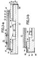
- a housing for the encapsulation of a component 3 consisting for example of an integrated electronic circuit formed on a wafer of semiconductor material, for example silicon.
- component means any passive or active component, discrete or integrated, as well as any electronic circuit (hybrid circuit for example) capable of being placed in a housing.
- the housing of Figure la mainly consists of a base 1, carrying the component 3, and a cover constituted by the distribution device 4 according to the invention.
- a base 1 carrying the component 3
- a cover constituted by the distribution device 4 according to the invention By way of example, there is shown a case of the "CHIP CARRIER" type.
- the base 1 is made of a material which must be usually rigid, preferably electrically insulating and having certain thermal qualities such as good thermal conduction and a coefficient of expansion as close as possible to that of component 3. It is for example plastic, glass, ceramic etc ...; in the case where component 3 is made of silicon, the base can advantageously be made of alumina.
- the base consists, in the example shown, of three distinct parts, marked respectively 11, 12 and 13.
- the first part 11 is in the form of a plate and supports the component 3; the other two parts each consist of a ring, the rings being concentric and arranged one above the other, around the component 3, with an increasing internal diameter, so as to allow the electrical connections between the component , the distributor 4 and the exterior.
- Component 3 is therefore fixed to the upper face of the wafer 11, for example by soldering onto a metallization shown in thick lines.
- Tracks and connections 61 to 65 are for example made from refractory metal (tungsten for example).
- the distribution device 4 consists of one or more conducting planes, depending on the number of potentials supply to distribute to component 3.
- the periphery of the plate 4 has half-holes 43 similar to the half-holes 14 of the base.
- the materials used to produce the conductive planes 41 or 42 are chosen so that they have a high electrical conductivity.
- refractory conductive materials such as tungsten, moly-manganese or molybdenum-tungsten are placed by screen printing on alumina layers and the whole is baked; according to another operating mode, a cooked alumina substrate is used on which metallic planes such as silver-palladium, copper, gold or gold-platinum are placed by screen printing, each covered with '' an electrical insulator based on glass (glass containing lead oxide) and crystal charges such as alumina.
- a stack of the multilayer printed circuit type is used, the insulating parts being made of epoxy glass for example or based on polyimide, and the conductive parts made of copper.
- Figure 2 there is shown an example of arrangement of the various conductive planes of Figure la. Still by way of example, the device 4 comprises three conducting planes.
- the conductive plane 42 connected for example to the ground, is of dimensions slightly smaller than those of the device 4 and is extended by tongues 421 towards the periphery of the device.
- the plane 41 connected for example to a supply potential, is provided with tongues 411, placed as close as possible to the tongues of mass 421 and preferably in equal numbers.
- the plane 46 connected to another supply potential, also includes tongues, marked 461 and in a number equal to the previous ones, so as to form groups of three tongues 411, 421, 461, in as large a number as necessary for the distribution of the potentials from device 4 to component 3.
- a structure has thus been produced in which the ground connections and two supply potentials are distributed around the periphery of the device 4, making it possible to reduce the inductance of the inputs-outputs since the ground connection is placed between the connections of food, as close as possible to each other.
- the device 4 is fixed (FIG. 1a) by means of a sealing ring 6 to the upper part of the base 1.
- the connections such as 44 are located outside of the sealing ring 6.
- the distribution device 4 is provided with one or more discrete decoupling capacitors 5, placed in FIG. 1a on the upper (external) face of the device 4; they are connected between two conductive planes, one of which is connected to ground, using conductive wells 51 and 52, passing through the insulator 40 and, if necessary, in isolation one or more conductive planes such as 41 or 42, and connection pads 53.
- Figures 3, a and b show a second embodiment of the invention in which the distribution device is located inside the housing.
- the component 3 carried by the base 1 is, for example, constituted by three rings and no longer two, deposited on the wafer 11, the third ring being marked 15.
- the distribution device 4 is arranged on the upper face of the second ring (13) and connected as illustrated in Figures 3a and 3b, similar to Figures la and Ib.
- the third ring . (15) is disposed at the periphery of the device 4 and receives a cover 2 of the housing, fixed to the base 1 by means of a seal 21.
- This cover may be metallic or insulating, made or not of the same material as the base 1.
- the device 4 has not been detailed in FIGS. 3 (a and b) but it is produced as described above and can also carry discrete capacitors such as 5.
- the cover 2 can also carry such capacitors.
- FIGS. 3 is a little more complex than that of FIGS. 1, but it allows the connections of the device 4 and the tight sealing of the cover to the base of the housing to be made separately, which is an advantage in some practical cases.
- Figure 4a shows a variant in the arrangement of the capacitor 5 on the distribution device 4 of the previous figures.
- FIG. 4b represents another variant of the positioning of the decoupling capacitor 5.
- the capacitor is placed on the lower face (46) of the device 4 in the same way as it was placed on the upper face of this same device in FIG.
- the underside 46 of the device 4 may have a recess such as 45 (FIG. 4a) to allow the capacitor 5 to be placed without it exceeding the level of the surface.
- Figures 5, a, b and c show different variants of the connection of the distribution device 4 to the rest of the housing.
- FIG. 5a we find the same configuration by way of example as that represented in FIG. 1a (left part), namely a three-stage base 1, carrying a component 3 and a distribution device 4, connected to the component 3 via tracks 61, 62 and connection wire 60.
- connection pin 70 disposed in a metallized hole 71, itself formed in the device 4.
- the conductive plane 41 is in electrical contact with the metallized hole 71.
- the connection pin 70 is integral with the base 1 (disc 73) and welded to the upper face of the device 4 (solder 72).
- the sealing ring 6 is placed inside the housing with respect to the pin 70.
- the conducting plane 42 is connected to another metallized hole, not visible in the figure.
- FIG. 5b shows another variant of connection of the distribution device 4 to the base 1.
- the variant of FIG. 5b has in particular the advantage of minimizing the length of the connections between the elements 3 and 4, which makes it possible to reduce the inductance and consequently the impedance of these connections; as is known, this is particularly sought in the case of circuits with low potentials and low response times.
- FIG. 5c shows another variant of connection of the distribution device 4, in which the latter is placed on the upper face of the penultimate stage of the base 1, by means of the sealing ring 6.
- the electrical connection is made by means of a metallic bridge 78, sealed or brazed (76) on the one hand on the upper face of the device 4 and on the other hand on the upper face of the base 1, in line with the connection 62.
- the connection planes 41 (for example) are connected to the metal bridge via elements 77 and 76.
- decoupling capacitors such as 5 for clarity of the diagram but these can of course be added according to one of the variants described above.
- a distribution device has been produced in the context of the digital example given above, with the following dimensions: length and width equal to 24mm, thickness of the order of 0, 5 to 1 mm for three conducting planes, the thickness of the conducting planes being of the order of ten microns.
- the components 5 have been described as discrete capacitors intended for decoupling, but they can be constituted by any component, discrete or integrated, necessary for the application.
Landscapes
- Fixed Capacitors And Capacitor Manufacturing Machines (AREA)
- Structures For Mounting Electric Components On Printed Circuit Boards (AREA)
- Lead Frames For Integrated Circuits (AREA)
Applications Claiming Priority (2)
| Application Number | Priority Date | Filing Date | Title |
|---|---|---|---|
| FR8408247 | 1984-05-25 | ||
| FR8408247A FR2565032B1 (fr) | 1984-05-25 | 1984-05-25 | Dispositif de repartition de potentiel electrique et boitier de composant electronique incorporant un tel dispositif |
Publications (2)
| Publication Number | Publication Date |
|---|---|
| EP0166634A1 true EP0166634A1 (de) | 1986-01-02 |
| EP0166634B1 EP0166634B1 (de) | 1990-10-03 |
Family
ID=9304410
Family Applications (1)
| Application Number | Title | Priority Date | Filing Date |
|---|---|---|---|
| EP85400992A Expired - Lifetime EP0166634B1 (de) | 1984-05-25 | 1985-05-21 | Einrichtung zur Verteilung von elektrischen Potentialen, und eine solche Einrichtung enthaltendes Gehäuse für elektronische Komponenten |
Country Status (4)
| Country | Link |
|---|---|
| EP (1) | EP0166634B1 (de) |
| JP (1) | JPS6139551A (de) |
| DE (1) | DE3579958D1 (de) |
| FR (1) | FR2565032B1 (de) |
Cited By (7)
| Publication number | Priority date | Publication date | Assignee | Title |
|---|---|---|---|---|
| US4695870A (en) * | 1986-03-27 | 1987-09-22 | Hughes Aircraft Company | Inverted chip carrier |
| EP0239494A1 (de) * | 1986-03-28 | 1987-09-30 | Bull S.A. | Gehäuse für integrierte Schaltung |
| GB2197540A (en) * | 1986-11-12 | 1988-05-18 | Murata Manufacturing Co | Circuit substrate |
| GB2201546A (en) * | 1987-01-20 | 1988-09-01 | Toshiba Kk | Semiconductor integrated circuit device |
| FR2621173A1 (fr) * | 1987-09-29 | 1989-03-31 | Bull Sa | Boitier pour circuit integre de haute densite |
| EP0397391A3 (de) * | 1989-05-08 | 1991-12-04 | Samsung Electronics Co., Ltd. | Chippackung mit Kondensatordeckel |
| EP0361495A3 (de) * | 1988-09-30 | 1992-03-18 | Hitachi, Ltd. | Halbleiterpackung und Computer, die diese Packung benutzt |
Families Citing this family (3)
| Publication number | Priority date | Publication date | Assignee | Title |
|---|---|---|---|---|
| FR2591801B1 (fr) * | 1985-12-17 | 1988-10-14 | Inf Milit Spatiale Aeronaut | Boitier d'encapsulation d'un circuit electronique |
| JPH0710650U (ja) * | 1993-07-26 | 1995-02-14 | 株式会社小松製作所 | 全油圧式ステアリングシステムの方向制御弁 |
| FR2940521B1 (fr) | 2008-12-19 | 2011-11-11 | 3D Plus | Procede de fabrication collective de modules electroniques pour montage en surface |
Citations (3)
| Publication number | Priority date | Publication date | Assignee | Title |
|---|---|---|---|---|
| US4249196A (en) * | 1978-08-21 | 1981-02-03 | Burroughs Corporation | Integrated circuit module with integral capacitor |
| FR2496341A1 (fr) * | 1980-12-12 | 1982-06-18 | Thomson Csf | Composant d'interconnexion topologique |
| FR2529386A1 (fr) * | 1982-06-29 | 1983-12-30 | Inf Milit Spatiale Aeronaut | Boitier de circuit electronique comportant un condensateur |
Family Cites Families (3)
| Publication number | Priority date | Publication date | Assignee | Title |
|---|---|---|---|---|
| JPS5582454A (en) * | 1978-12-15 | 1980-06-21 | Toshiba Corp | Container for integrated circuit element |
| JPS5764953A (en) * | 1980-10-09 | 1982-04-20 | Oki Electric Ind Co Ltd | Semiconductor device |
| JPS57113261A (en) * | 1980-12-29 | 1982-07-14 | Nec Corp | Semiconductor device |
-
1984
- 1984-05-25 FR FR8408247A patent/FR2565032B1/fr not_active Expired
-
1985
- 1985-05-21 EP EP85400992A patent/EP0166634B1/de not_active Expired - Lifetime
- 1985-05-21 DE DE8585400992T patent/DE3579958D1/de not_active Expired - Fee Related
- 1985-05-24 JP JP11197385A patent/JPS6139551A/ja active Pending
Patent Citations (3)
| Publication number | Priority date | Publication date | Assignee | Title |
|---|---|---|---|---|
| US4249196A (en) * | 1978-08-21 | 1981-02-03 | Burroughs Corporation | Integrated circuit module with integral capacitor |
| FR2496341A1 (fr) * | 1980-12-12 | 1982-06-18 | Thomson Csf | Composant d'interconnexion topologique |
| FR2529386A1 (fr) * | 1982-06-29 | 1983-12-30 | Inf Milit Spatiale Aeronaut | Boitier de circuit electronique comportant un condensateur |
Non-Patent Citations (2)
| Title |
|---|
| IEEE TRANSACTIONS ON COMPONENTS, HYBRIDS, AND MANUFACTURING TECHNOLOGY, vol. CHMT-6, no. 3, septembre 1983, pages 283-289, IEEE, New York, US; L.W. SCHAPER et al.: "Improved electrical performance required for future MOS packaging" * |
| PATENTS ABSTRACTS OF JAPAN, vol. 6, no. 205 (E-136) [1083], 16 octobre 1982, page 115 E 136; & JP - A - 57 113 261 (NIPPON DENKI K.K.) 14-07-1982 * |
Cited By (13)
| Publication number | Priority date | Publication date | Assignee | Title |
|---|---|---|---|---|
| US4695870A (en) * | 1986-03-27 | 1987-09-22 | Hughes Aircraft Company | Inverted chip carrier |
| US4812949A (en) * | 1986-03-28 | 1989-03-14 | Bull, S.A. | Method of and apparatus for mounting an IC chip |
| EP0239494A1 (de) * | 1986-03-28 | 1987-09-30 | Bull S.A. | Gehäuse für integrierte Schaltung |
| FR2596607A1 (fr) * | 1986-03-28 | 1987-10-02 | Bull Sa | Procede de montage d'un circuit integre sur une carte de circuits imprimes, boitier de circuit integre en resultant et ruban porteur de circuits integres pour la mise en oeuvre du procede |
| GB2197540A (en) * | 1986-11-12 | 1988-05-18 | Murata Manufacturing Co | Circuit substrate |
| US4800459A (en) * | 1986-11-12 | 1989-01-24 | Murata Manufacturing Co., Ltd. | Circuit substrate having ceramic multilayer structure containing chip-like electronic components |
| GB2197540B (en) * | 1986-11-12 | 1991-04-17 | Murata Manufacturing Co | A circuit structure. |
| GB2201546A (en) * | 1987-01-20 | 1988-09-01 | Toshiba Kk | Semiconductor integrated circuit device |
| GB2201546B (en) * | 1987-01-20 | 1990-05-09 | Toshiba Kk | Semiconductor integrated circuit device |
| FR2621173A1 (fr) * | 1987-09-29 | 1989-03-31 | Bull Sa | Boitier pour circuit integre de haute densite |
| EP0310463A1 (de) * | 1987-09-29 | 1989-04-05 | Bull S.A. | Gehäuse für einen hochintegrierten Schaltkreis |
| EP0361495A3 (de) * | 1988-09-30 | 1992-03-18 | Hitachi, Ltd. | Halbleiterpackung und Computer, die diese Packung benutzt |
| EP0397391A3 (de) * | 1989-05-08 | 1991-12-04 | Samsung Electronics Co., Ltd. | Chippackung mit Kondensatordeckel |
Also Published As
| Publication number | Publication date |
|---|---|
| FR2565032B1 (fr) | 1987-02-20 |
| DE3579958D1 (de) | 1990-11-08 |
| JPS6139551A (ja) | 1986-02-25 |
| FR2565032A1 (fr) | 1985-11-29 |
| EP0166634B1 (de) | 1990-10-03 |
Similar Documents
| Publication | Publication Date | Title |
|---|---|---|
| EP0133125B1 (de) | Gehäuse für einen elektronischen Baustein mit einem Kondensator | |
| EP0228953B1 (de) | Verkapselungsgehäuse für eine elektronische Schaltung | |
| US5523622A (en) | Semiconductor integrated device having parallel signal lines | |
| EP0583201B1 (de) | Dreidimensionaler Mehrchipmodul | |
| EP0310463A1 (de) | Gehäuse für einen hochintegrierten Schaltkreis | |
| EP0108098A1 (de) | Schutzelemente für elektronische bauteile gegen spannungen verursacht durch ein elektromagnetisches feld | |
| EP0565391A1 (de) | Verfahren und Vorrichtung zur Verkapselung von dreidimensionalen Halbleiterplättchen | |
| EP0166634B1 (de) | Einrichtung zur Verteilung von elektrischen Potentialen, und eine solche Einrichtung enthaltendes Gehäuse für elektronische Komponenten | |
| FR2518811A1 (fr) | Dispositif a circuit integre en conteneur de ceramique | |
| FR2645681A1 (fr) | Dispositif d'interconnexion verticale de pastilles de circuits integres et son procede de fabrication | |
| FR2849538A1 (fr) | Composant discret comprenant des diodes hf en serie et a cathode commune | |
| EP0346206A1 (de) | Aktiver Verbinder für Leiterplatten | |
| FR2629667A1 (fr) | Dispositif a circuit imprime | |
| EP0334747A1 (de) | Vorrichtung zur Verbindung und für den Schutz eines unbedeckten Chips eines Hochfrequenzbauteils | |
| FR2489592A1 (fr) | Micro-boitier ceramique d'encapsulation de circuit electronique | |
| FR2529386A1 (fr) | Boitier de circuit electronique comportant un condensateur | |
| FR2620275A1 (fr) | Boitier pour le montage en surface d'un composant fonctionnant en hyperfrequences | |
| EP0030168B1 (de) | Vorrichtung zur Parallelschaltung von Höchstfrequenz-Leistungstransistoren | |
| FR2584865A1 (fr) | Composant electronique comportant un condensateur | |
| EP0282396A1 (de) | Komplexe Hybridschaltungsstruktur und Verfahren zur Herstellung | |
| EP0484853A1 (de) | Verfahren zum Schützen der elektronischen Bausteine einer Schaltung gegen die Strahlungen und Vorrichtung nach dem Verfahren | |
| EP0356266B1 (de) | Kompakter Filter mit Resonatoren und mit Verwendung des piezoelektrischen Effektes | |
| FR2879348A1 (fr) | Protection d'un condensateur integre | |
| JPH03250659A (ja) | 半導体素子収納用パッケージ | |
| KR100381841B1 (ko) | 반도체패키지 및 그 제조 방법 |
Legal Events
| Date | Code | Title | Description |
|---|---|---|---|
| PUAI | Public reference made under article 153(3) epc to a published international application that has entered the european phase |
Free format text: ORIGINAL CODE: 0009012 |
|
| AK | Designated contracting states |
Designated state(s): DE GB IT NL SE |
|
| 17P | Request for examination filed |
Effective date: 19860614 |
|
| 17Q | First examination report despatched |
Effective date: 19880629 |
|
| GRAA | (expected) grant |
Free format text: ORIGINAL CODE: 0009210 |
|
| RAP1 | Party data changed (applicant data changed or rights of an application transferred) |
Owner name: THOMSON-CSF |
|
| AK | Designated contracting states |
Kind code of ref document: B1 Designated state(s): DE GB IT NL SE |
|
| ITF | It: translation for a ep patent filed | ||
| REF | Corresponds to: |
Ref document number: 3579958 Country of ref document: DE Date of ref document: 19901108 |
|
| GBT | Gb: translation of ep patent filed (gb section 77(6)(a)/1977) | ||
| PLBE | No opposition filed within time limit |
Free format text: ORIGINAL CODE: 0009261 |
|
| STAA | Information on the status of an ep patent application or granted ep patent |
Free format text: STATUS: NO OPPOSITION FILED WITHIN TIME LIMIT |
|
| 26N | No opposition filed | ||
| PGFP | Annual fee paid to national office [announced via postgrant information from national office to epo] |
Ref country code: SE Payment date: 19930419 Year of fee payment: 9 |
|
| PGFP | Annual fee paid to national office [announced via postgrant information from national office to epo] |
Ref country code: DE Payment date: 19930420 Year of fee payment: 9 |
|
| PGFP | Annual fee paid to national office [announced via postgrant information from national office to epo] |
Ref country code: GB Payment date: 19930422 Year of fee payment: 9 |
|
| ITTA | It: last paid annual fee | ||
| PGFP | Annual fee paid to national office [announced via postgrant information from national office to epo] |
Ref country code: NL Payment date: 19930531 Year of fee payment: 9 |
|
| PG25 | Lapsed in a contracting state [announced via postgrant information from national office to epo] |
Ref country code: GB Effective date: 19940521 |
|
| PG25 | Lapsed in a contracting state [announced via postgrant information from national office to epo] |
Ref country code: SE Effective date: 19940522 |
|
| PG25 | Lapsed in a contracting state [announced via postgrant information from national office to epo] |
Ref country code: NL Effective date: 19941201 |
|
| NLV4 | Nl: lapsed or anulled due to non-payment of the annual fee | ||
| GBPC | Gb: european patent ceased through non-payment of renewal fee |
Effective date: 19940521 |
|
| EUG | Se: european patent has lapsed |
Ref document number: 85400992.5 Effective date: 19941210 |
|
| PG25 | Lapsed in a contracting state [announced via postgrant information from national office to epo] |
Ref country code: DE Effective date: 19950201 |
|
| EUG | Se: european patent has lapsed |
Ref document number: 85400992.5 |