EP0269613A2 - Dispositif de lithographie par projection d'ions - Google Patents
Dispositif de lithographie par projection d'ions Download PDFInfo
- Publication number
- EP0269613A2 EP0269613A2 EP19870890272 EP87890272A EP0269613A2 EP 0269613 A2 EP0269613 A2 EP 0269613A2 EP 19870890272 EP19870890272 EP 19870890272 EP 87890272 A EP87890272 A EP 87890272A EP 0269613 A2 EP0269613 A2 EP 0269613A2
- Authority
- EP
- European Patent Office
- Prior art keywords
- mask
- substrate
- ion
- multipole
- wafer
- Prior art date
- Legal status (The legal status is an assumption and is not a legal conclusion. Google has not performed a legal analysis and makes no representation as to the accuracy of the status listed.)
- Granted
Links
- 238000010884 ion-beam technique Methods 0.000 title claims description 7
- 238000001459 lithography Methods 0.000 title description 2
- 230000005405 multipole Effects 0.000 claims abstract description 19
- 239000000758 substrate Substances 0.000 claims description 26
- 230000003287 optical effect Effects 0.000 abstract description 7
- 238000012937 correction Methods 0.000 abstract description 5
- 150000002500 ions Chemical class 0.000 description 27
- 235000012431 wafers Nutrition 0.000 description 15
- 238000000034 method Methods 0.000 description 6
- 229910052732 germanium Inorganic materials 0.000 description 4
- GNPVGFCGXDBREM-UHFFFAOYSA-N germanium atom Chemical compound [Ge] GNPVGFCGXDBREM-UHFFFAOYSA-N 0.000 description 4
- 229920002120 photoresistant polymer Polymers 0.000 description 4
- 238000006073 displacement reaction Methods 0.000 description 3
- 238000003384 imaging method Methods 0.000 description 3
- 238000000996 ion projection lithography Methods 0.000 description 3
- 238000012546 transfer Methods 0.000 description 3
- 230000003213 activating effect Effects 0.000 description 2
- 238000004519 manufacturing process Methods 0.000 description 2
- 239000004065 semiconductor Substances 0.000 description 2
- 241001461123 Matrona Species 0.000 description 1
- 235000006679 Mentha X verticillata Nutrition 0.000 description 1
- 235000002899 Mentha suaveolens Nutrition 0.000 description 1
- 235000001636 Mentha x rotundifolia Nutrition 0.000 description 1
- 230000004913 activation Effects 0.000 description 1
- 238000001514 detection method Methods 0.000 description 1
- 238000011161 development Methods 0.000 description 1
- 238000009826 distribution Methods 0.000 description 1
- 238000010894 electron beam technology Methods 0.000 description 1
- 238000002474 experimental method Methods 0.000 description 1
- 239000000463 material Substances 0.000 description 1
- 230000002093 peripheral effect Effects 0.000 description 1
- 238000001020 plasma etching Methods 0.000 description 1
- 229920003229 poly(methyl methacrylate) Polymers 0.000 description 1
- 239000004926 polymethyl methacrylate Substances 0.000 description 1
- 239000007787 solid Substances 0.000 description 1
- 230000003068 static effect Effects 0.000 description 1
- 238000012360 testing method Methods 0.000 description 1
Images

Classifications
-
- H—ELECTRICITY
- H01—ELECTRIC ELEMENTS
- H01J—ELECTRIC DISCHARGE TUBES OR DISCHARGE LAMPS
- H01J37/00—Discharge tubes with provision for introducing objects or material to be exposed to the discharge, e.g. for the purpose of examination or processing thereof
- H01J37/02—Details
- H01J37/04—Arrangements of electrodes and associated parts for generating or controlling the discharge, e.g. electron-optical arrangement or ion-optical arrangement
- H01J37/147—Arrangements for directing or deflecting the discharge along a desired path
- H01J37/1472—Deflecting along given lines
- H01J37/1474—Scanning means
- H01J37/1477—Scanning means electrostatic
-
- H—ELECTRICITY
- H01—ELECTRIC ELEMENTS
- H01J—ELECTRIC DISCHARGE TUBES OR DISCHARGE LAMPS
- H01J37/00—Discharge tubes with provision for introducing objects or material to be exposed to the discharge, e.g. for the purpose of examination or processing thereof
- H01J37/30—Electron-beam or ion-beam tubes for localised treatment of objects
- H01J37/3002—Details
- H01J37/3007—Electron or ion-optical systems
Definitions
- the invention relates to an ion projection device in which at least one device for generating an electrostatic deflection field and a mask with physical openings (so-called "open stencil” mask) are arranged in the beam path between the ion source and the substrate (wafer).
- at least one device for generating an electrostatic deflection field and a mask with physical openings are arranged in the beam path between the ion source and the substrate (wafer).
- the object of the invention is to provide possibilities for electronic distortion correction or setting and scale setting for an image whose scale is essentially 1: 1 (shadow projection).
- open-stencil masks often have certain distortions, that is to say shifting the position of the mask openings relative to their desired positions. If, as is customary in the production of semiconductor circuits, different masks are imaged on the same substrate surface in different projection steps, the different masks will generally have different distortion states. This can lead to intolerable displacements of the structures that originate from one mask in relation to structures that originate from another mask. It is therefore necessary to compensate for the distortion of each mask during the imaging so that only tolerable dislocations occur.
- the structuring of a semiconductor switching element is carried out on two or more different systems, for example the coarser structuring with an optical wafer stepper that is cheaper in operation and the finer one in an ion projection system.
- the imaging of the masks used in the ion projection system must be adapted to the distortion state of the structures produced in the optical wafer stepper, i.e. The position of the openings in the mask must be changed (distorted) in the figure.
- an electrostatic multipole in front of the mask. This should have at least eight, but preferably more, poles. If this multipole is activated, depending on the setting of the applied voltages, an inhomogeneous deflection of the partial beams passing through the mask openings is achieved, and the deflected partial beam hits the mask at a changed angle, so that the silhouette of the mask openings on the wafer is located below the mask is located, is changed.
- a homogeneous deflection of all partial beams can also be achieved.
- the substrate is arranged at a large distance from the mask, this distance being able to be in the order of 5 to 10 mm, for example.
- the diameter must also be according to the above equation the source is reduced and / or the distance of the mask from the source is increased. This measure makes it possible to achieve a relatively large change in position of the image on the substrate with a relatively small deflection of the beam. Minor distractions should be aimed at in order to keep unfavorable influences (distortions), which can be caused by the electrical peripheral fields of the correction element, small.
- a device for generating an axial magnetic field e.g. a coil arranged coaxially to the optical axis.
- rotations of the image can be carried out so that the resulting changes in position allow the structures to be produced by ion lithography to be correspondingly covered with structures already present on the wafer.
- A, in particular mechanical, shutter can be arranged in the space between the mask and the substrate, the so-called proximity gap. This offers the possibility, even during changes in the position of the wafer, in which time exposure of the wafer has to be omitted, to further expose the mask to the ion beam and in this way to keep its temperature constant, as a result of which possible changes in position of mask openings, as can otherwise occur with temperature fluctuations, are certain can be kept within the required tolerances.
- electronic detectors can be arranged in the space between the mask and the substrate, which serve to detect the position of the substrate or the position of structures on the substrate.
- the partial beams which pass through the mask opening can then be controlled by means of the multipole until the position of the structures produced by ion projection on the substrate assume the desired target position. In this way, it is possible to align existing structures on the wafer with new structures to be created.
- a Scale setting can be carried out.
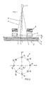
- 1 denotes an ion source, preferably a duoplas matron ion source, from which a divergent ion beam 9 is emitted.
- a mask 4 with mask openings 11, which is held in a holder 6, is located below this ion source at a distance of, for example, 500 mm.
- a substrate (wafer) 2 Under the mask 4, at a distance s, is a substrate (wafer) 2.
- the substrate can be an Si wafer with a corresponding layer structure 7.
- the wafer 2 can be covered, for example, with a three-layer resist (photoresist) layer 8, for example 1 ⁇ m AZ photoresist as the base layer, a 30 nm evaporated germanium layer as the intermediate layer and a thin photoresist as the top layer.
- a three-layer resist (photoresist) layer 8 for example 1 ⁇ m AZ photoresist as the base layer, a 30 nm evaporated germanium layer as the intermediate layer and a thin photoresist as the top layer.
- the top resist layer is developed, which then serves as a mask for the structure transfer, for example by the known reactive ion etching technique.
- the top layer was omitted and the exposure with 5 keV He+ ions was carried out directly into the germanium layer.
- the germanium layer After exposure, the irradiated areas of the germanium layer could be negatively developed in a CF4 plasma.
- an electrostatic multipole e.g. an octopole 3.
- the term "immediately” does not limit the distance of the multipole from the mask. For example, a distance of 10 cm between a multipole and the mask can be considered “immediate” in the sense of the above statements.
- a device for generating an axial magnetic field can also be assigned to the multipole 3.
- a coil arranged coaxially to the optical axis can be used for this. This can also be integrated in the multipole 3.
- a mechanical shutter can be arranged there.
- the mask 4 can also be irradiated with ions when the substrate 2 is not to be irradiated, so that the temperature of the mask is constant and the position of the mask openings is also maintained.
- electronic detectors for detecting the position of the substrate or for Detecting the position of the substrate or for detecting the position of structures located on the substrate. This is of particular importance if the ion projection lithography device is used as an ion stepper, together with optical wafer steppers or also with electron or X-ray steppers.
- wafers that have already been provided with structures in optical or other (e.g. X-ray) steppers are to be further processed in the ion projection devices described, it would be necessary to produce a corresponding alignment between the already existing structures and the structures to be produced in the ion projection lithography device. This is achieved in the x, y direction and rotation and scale (the z direction is defined as the direction of the ion-optical axis) by means of the device designed according to the invention.
- Fig. 2 shows schematically an octopole with applied potentials U1 ?? U8.
- U1 U0
- U2 U0 / ⁇ 2
- U3 O
- U4 -U0 / ⁇ 2
- U5 -U0
- U6 -U0 / ⁇ 2
- U7 O
- U8 U0 / ⁇ 2
- U0 U0.cos (- ⁇ )
- U0 is selected according to the ion energy, the desired displacement in the x-direction and the distance s mask-wafer.
- the specified potentials must be selected U1 Hence U8 components
- U i ⁇ U0 ⁇ . Sin ⁇ i are added.
- FIG. 3 illustrates the image of a square mask, the pixels being marked with A, B, C and D are labeled and the square sides appear as curved lines.
- FIG. 4 shows how the shifting of the corner points takes place with fully marked lines.
- An ion beam 10 is drawn here, which reaches the opening 11 of the mask 4 without activating the multipole 3. These rays would occupy an area EF on the substrate 2.
- the beam strikes the opening 11 of the mask 4 at a different angle of incidence and fulfills the area E ⁇ -F ⁇ on the substrate 2, which is shifted to the left relative to the area EF (in FIG. 3).
Landscapes
- Chemical & Material Sciences (AREA)
- Analytical Chemistry (AREA)
- Electron Beam Exposure (AREA)
- Cathode-Ray Tubes And Fluorescent Screens For Display (AREA)
- Electron Sources, Ion Sources (AREA)
- Physical Vapour Deposition (AREA)
- Exposure And Positioning Against Photoresist Photosensitive Materials (AREA)
Applications Claiming Priority (2)
| Application Number | Priority Date | Filing Date | Title |
|---|---|---|---|
| AT3173/86 | 1986-11-27 | ||
| AT3173/86A AT393333B (de) | 1986-11-27 | 1986-11-27 | Ionenprojektionseinrichtung fuer schattenprojektion |
Publications (3)
| Publication Number | Publication Date |
|---|---|
| EP0269613A2 true EP0269613A2 (fr) | 1988-06-01 |
| EP0269613A3 EP0269613A3 (en) | 1989-01-11 |
| EP0269613B1 EP0269613B1 (fr) | 1992-06-17 |
Family
ID=3546471
Family Applications (1)
| Application Number | Title | Priority Date | Filing Date |
|---|---|---|---|
| EP87890272A Expired - Lifetime EP0269613B1 (fr) | 1986-11-27 | 1987-11-26 | Dispositif de lithographie par projection d'ions |
Country Status (5)
| Country | Link |
|---|---|
| US (1) | US4835392A (fr) |
| EP (1) | EP0269613B1 (fr) |
| JP (1) | JPS63276859A (fr) |
| AT (2) | AT393333B (fr) |
| DE (1) | DE3779876D1 (fr) |
Families Citing this family (5)
| Publication number | Priority date | Publication date | Assignee | Title |
|---|---|---|---|---|
| JPH0774838B2 (ja) * | 1991-03-26 | 1995-08-09 | 工業技術院長 | 荷電粒子の捕獲方法及び装置 |
| JPH07112539B2 (ja) * | 1992-04-15 | 1995-12-06 | 工業技術院長 | 微小粒子の作製方法及びその装置 |
| EP0731490A3 (fr) * | 1995-03-02 | 1998-03-11 | Ebara Corporation | Procédé de microfabrication ultra-fine utilisant un faisceau d'énergie |
| EP0732624B1 (fr) * | 1995-03-17 | 2001-10-10 | Ebara Corporation | Méthode de fabrication utilisant un faisceau d'énergie |
| US6335534B1 (en) * | 1998-04-17 | 2002-01-01 | Kabushiki Kaisha Toshiba | Ion implantation apparatus, ion generating apparatus and semiconductor manufacturing method with ion implantation processes |
Family Cites Families (11)
| Publication number | Priority date | Publication date | Assignee | Title |
|---|---|---|---|---|
| US3845312A (en) * | 1972-07-13 | 1974-10-29 | Texas Instruments Inc | Particle accelerator producing a uniformly expanded particle beam of uniform cross-sectioned density |
| US4158141A (en) * | 1978-06-21 | 1979-06-12 | Hughes Aircraft Company | Process for channeling ion beams |
| AT371947B (de) * | 1979-12-27 | 1983-08-10 | Rudolf Sacher Ges M B H | Freitragende maske, verfahren zur herstellung derselben und verfahren zum maskieren von substraten |
| DE3035200C2 (de) * | 1980-09-18 | 1982-09-02 | Fraunhofer-Gesellschaft zur Förderung der angewandten Forschung e.V., 8000 München | Maske für die Ionenstrahl-Schattenprojektion |
| JPS5769653A (en) * | 1980-10-20 | 1982-04-28 | Fujitsu Ltd | Charged particle beam device |
| US4385238A (en) * | 1981-03-03 | 1983-05-24 | Veeco Instruments Incorporated | Reregistration system for a charged particle beam exposure system |
| DE3138896A1 (de) * | 1981-09-30 | 1983-04-14 | Siemens AG, 1000 Berlin und 8000 München | Elektronenoptisches system mit vario-formstrahl zur erzeugung und messung von mikrostrukturen |
| JPS5946744A (ja) * | 1982-09-08 | 1984-03-16 | Rikagaku Kenkyusho | 多重極電極構造体 |
| FR2556501B1 (fr) * | 1983-12-09 | 1986-08-01 | Golanski Andrzej | Procede et dispositif de traitement thermique de plaquettes et semiconducteurs |
| JPH0732111B2 (ja) * | 1985-06-10 | 1995-04-10 | 日本電信電話株式会社 | 荷電ビ−ム投影露光装置 |
| US4757208A (en) * | 1986-03-07 | 1988-07-12 | Hughes Aircraft Company | Masked ion beam lithography system and method |
-
1986
- 1986-11-27 AT AT3173/86A patent/AT393333B/de not_active IP Right Cessation
-
1987
- 1987-11-20 US US07/123,128 patent/US4835392A/en not_active Expired - Fee Related
- 1987-11-25 JP JP62297292A patent/JPS63276859A/ja active Pending
- 1987-11-26 DE DE8787890272T patent/DE3779876D1/de not_active Expired - Fee Related
- 1987-11-26 EP EP87890272A patent/EP0269613B1/fr not_active Expired - Lifetime
- 1987-11-26 AT AT87890272T patent/ATE77513T1/de not_active IP Right Cessation
Non-Patent Citations (1)
| Title |
|---|
| JOURNAL OF VACUUM SCIENCE & TECHNOLOGY/A, Band 4, Nr. 3, Teil 1, Mai-Juni 1986, Seiten 777-783, American Vacuum Society, Woodbury, N.Y., US; J.N. RANDALL: Prospects for printing very large scale integrated circuits with masked ion beam lithography" * |
Also Published As
| Publication number | Publication date |
|---|---|
| US4835392A (en) | 1989-05-30 |
| AT393333B (de) | 1991-09-25 |
| ATE77513T1 (de) | 1992-07-15 |
| EP0269613A3 (en) | 1989-01-11 |
| DE3779876D1 (de) | 1992-07-23 |
| ATA317386A (de) | 1991-02-15 |
| EP0269613B1 (fr) | 1992-06-17 |
| JPS63276859A (ja) | 1988-11-15 |
Similar Documents
| Publication | Publication Date | Title |
|---|---|---|
| DE19848070B4 (de) | Niedrigenergie-Elektronenstrahllithographie | |
| EP0294363B1 (fr) | Méthode et dispositif pour positionner et aligner la structure d'image d'un masque sur un substrat | |
| DE2727733C2 (de) | Elektronenstrahllithographieanordnung | |
| DE2739502C3 (de) | Verfahren zur Belichtung durch Korpuskularstrahlen-Schattenwurf und Vorrichtung zur Durchführung des Verfahrens | |
| DE69123677T2 (de) | Reflektionsmaske und eine solche Reflektionsmaske verwendendes geladenes Teilchenstrahl-Belichtungsgerät | |
| DE69315758T2 (de) | Implantationsgerät mittels fokusierten Ionenstrahls | |
| EP0134269B1 (fr) | Lithographie par faisceau d'électrons par projection | |
| DE2832582A1 (de) | Elektronenlinsenanordnung fuer grossflaechige elektronenstrahl-abtastung | |
| EP0069823B1 (fr) | Procédé et dispositif pour le positionnement (mise en registre) mutuel des objets en lithographie à rayons X et rayons ioniques | |
| DE68925266T2 (de) | Korpuskularbestrahlungsverfahren mit einer Maske | |
| EP0106154B1 (fr) | Objectif déflecteur de faisceau de particules neutres à forme variable et procédé pour son utilisation | |
| DE3703516A1 (de) | Verfahren und vorrichtung zum ausrichten | |
| EP0231164B1 (fr) | Dispositif pour appareils de projection ionique | |
| EP0269613B1 (fr) | Dispositif de lithographie par projection d'ions | |
| EP0216750B1 (fr) | Appareil à faisceau ionique et procédé pour effectuer des modifications, en particulier des réparations sur des substrats à l'aide d'un appareil à faisceau ionique | |
| EP0739531B1 (fr) | Systeme de reproduction optique par faisceaux de particules | |
| EP0523033A1 (fr) | Système d'imagerie en optique ionique | |
| DE2460715C3 (de) | Korpuskularstrahloptisches Gerät zur Korpuskelbestrahlung eines Präparats in Form eines Flächenmusters mit mehreren untereinander gleichen Flächenelementen | |
| DE102007063649B4 (de) | Verfahren zum Erzeugen von Strukturen in einem Resistmaterial und Elektronenstrahlbelichtungsanlagen | |
| DE102004012240B4 (de) | Verfahren zur Herstellung einer Lochmaske zur lithographischen Strukturierung mittels geladener Teilchen | |
| DE2108669A1 (de) | Verfahren zur bestrahlung eines selek tierten Gebietes einer Oberflache eines Werk Stuckes mit geladenen Teilchen | |
| DE2852961C2 (fr) | ||
| EP0528785A1 (fr) | Système d'imagerie en optique ionique | |
| DE3138744A1 (de) | Verfahren zum herstellen von halbleitervorrichtungen | |
| DE10392343T5 (de) | Maske, Herstellungsverfahren für Halbleitereinrichtung und Halbleitereinrichtung |
Legal Events
| Date | Code | Title | Description |
|---|---|---|---|
| PUAI | Public reference made under article 153(3) epc to a published international application that has entered the european phase |
Free format text: ORIGINAL CODE: 0009012 |
|
| AK | Designated contracting states |
Kind code of ref document: A2 Designated state(s): AT BE DE FR GB IT NL SE |
|
| PUAL | Search report despatched |
Free format text: ORIGINAL CODE: 0009013 |
|
| AK | Designated contracting states |
Kind code of ref document: A3 Designated state(s): AT BE DE FR GB IT NL SE |
|
| 17P | Request for examination filed |
Effective date: 19890328 |
|
| RAP1 | Party data changed (applicant data changed or rights of an application transferred) |
Owner name: OESTERREICHISCHE INVESTITIONSKREDIT AKTIENGESELLS Owner name: IMS IONEN MIKROFABRIKATIONS SYSTEME GESELLSCHAFT M |
|
| 17Q | First examination report despatched |
Effective date: 19910131 |
|
| GRAA | (expected) grant |
Free format text: ORIGINAL CODE: 0009210 |
|
| AK | Designated contracting states |
Kind code of ref document: B1 Designated state(s): AT BE DE FR GB IT NL SE |
|
| PG25 | Lapsed in a contracting state [announced via postgrant information from national office to epo] |
Ref country code: SE Effective date: 19920617 Ref country code: BE Effective date: 19920617 |
|
| REF | Corresponds to: |
Ref document number: 77513 Country of ref document: AT Date of ref document: 19920715 Kind code of ref document: T |
|
| RIN1 | Information on inventor provided before grant (corrected) |
Inventor name: LOESCHNER, HANS, DR. Inventor name: STENGL, GERHARD, DR. |
|
| REF | Corresponds to: |
Ref document number: 3779876 Country of ref document: DE Date of ref document: 19920723 |
|
| ITF | It: translation for a ep patent filed | ||
| GBT | Gb: translation of ep patent filed (gb section 77(6)(a)/1977) | ||
| ET | Fr: translation filed | ||
| PGFP | Annual fee paid to national office [announced via postgrant information from national office to epo] |
Ref country code: AT Payment date: 19921027 Year of fee payment: 6 |
|
| PGFP | Annual fee paid to national office [announced via postgrant information from national office to epo] |
Ref country code: NL Payment date: 19921130 Year of fee payment: 6 |
|
| PLBE | No opposition filed within time limit |
Free format text: ORIGINAL CODE: 0009261 |
|
| STAA | Information on the status of an ep patent application or granted ep patent |
Free format text: STATUS: NO OPPOSITION FILED WITHIN TIME LIMIT |
|
| 26N | No opposition filed | ||
| PG25 | Lapsed in a contracting state [announced via postgrant information from national office to epo] |
Ref country code: AT Effective date: 19931126 |
|
| PG25 | Lapsed in a contracting state [announced via postgrant information from national office to epo] |
Ref country code: NL Effective date: 19940601 |
|
| NLV4 | Nl: lapsed or anulled due to non-payment of the annual fee | ||
| PGFP | Annual fee paid to national office [announced via postgrant information from national office to epo] |
Ref country code: GB Payment date: 19981112 Year of fee payment: 12 Ref country code: FR Payment date: 19981112 Year of fee payment: 12 |
|
| PGFP | Annual fee paid to national office [announced via postgrant information from national office to epo] |
Ref country code: DE Payment date: 19981114 Year of fee payment: 12 |
|
| PG25 | Lapsed in a contracting state [announced via postgrant information from national office to epo] |
Ref country code: GB Free format text: LAPSE BECAUSE OF NON-PAYMENT OF DUE FEES Effective date: 19991126 |
|
| GBPC | Gb: european patent ceased through non-payment of renewal fee |
Effective date: 19991126 |
|
| PG25 | Lapsed in a contracting state [announced via postgrant information from national office to epo] |
Ref country code: FR Free format text: LAPSE BECAUSE OF NON-PAYMENT OF DUE FEES Effective date: 20000731 |
|
| PG25 | Lapsed in a contracting state [announced via postgrant information from national office to epo] |
Ref country code: DE Free format text: LAPSE BECAUSE OF NON-PAYMENT OF DUE FEES Effective date: 20000901 |
|
| REG | Reference to a national code |
Ref country code: FR Ref legal event code: ST |
|
| PG25 | Lapsed in a contracting state [announced via postgrant information from national office to epo] |
Ref country code: IT Free format text: LAPSE BECAUSE OF NON-PAYMENT OF DUE FEES;WARNING: LAPSES OF ITALIAN PATENTS WITH EFFECTIVE DATE BEFORE 2007 MAY HAVE OCCURRED AT ANY TIME BEFORE 2007. THE CORRECT EFFECTIVE DATE MAY BE DIFFERENT FROM THE ONE RECORDED. Effective date: 20051126 |