EP0271533B1 - Moyen de transport pour dispositifs electriques - Google Patents
Moyen de transport pour dispositifs electriques Download PDFInfo
- Publication number
- EP0271533B1 EP0271533B1 EP87903803A EP87903803A EP0271533B1 EP 0271533 B1 EP0271533 B1 EP 0271533B1 EP 87903803 A EP87903803 A EP 87903803A EP 87903803 A EP87903803 A EP 87903803A EP 0271533 B1 EP0271533 B1 EP 0271533B1
- Authority
- EP
- European Patent Office
- Prior art keywords
- carrier
- carrier unit
- frame
- transport medium
- carrier units
- Prior art date
- Legal status (The legal status is an assumption and is not a legal conclusion. Google has not performed a legal analysis and makes no representation as to the accuracy of the status listed.)
- Expired - Lifetime
Links
Images


Classifications
-
- H—ELECTRICITY
- H05—ELECTRIC TECHNIQUES NOT OTHERWISE PROVIDED FOR
- H05K—PRINTED CIRCUITS; CASINGS OR CONSTRUCTIONAL DETAILS OF ELECTRIC APPARATUS; MANUFACTURE OF ASSEMBLAGES OF ELECTRICAL COMPONENTS
- H05K13/00—Apparatus or processes specially adapted for manufacturing or adjusting assemblages of electric components
- H05K13/0084—Containers and magazines for components, e.g. tube-like magazines
-
- H—ELECTRICITY
- H10—SEMICONDUCTOR DEVICES; ELECTRIC SOLID-STATE DEVICES NOT OTHERWISE PROVIDED FOR
- H10P—GENERIC PROCESSES OR APPARATUS FOR THE MANUFACTURE OR TREATMENT OF DEVICES COVERED BY CLASS H10
- H10P72/00—Handling or holding of wafers, substrates or devices during manufacture or treatment thereof
- H10P72/70—Handling or holding of wafers, substrates or devices during manufacture or treatment thereof for supporting or gripping
- H10P72/74—Handling or holding of wafers, substrates or devices during manufacture or treatment thereof for supporting or gripping using temporarily an auxiliary support
- H10P72/741—Handling or holding of wafers, substrates or devices during manufacture or treatment thereof for supporting or gripping using temporarily an auxiliary support the auxiliary support including a cavity for storing a finished or partly finished device during manufacturing or mounting, e.g. for an IC package or for a chip
Definitions
- This invention relates to a transport medium for the in-processing transportation of electrical devices.
- the term "electrical device” shall refer to and mean semiconductor devices, integrated circuit devices, hybrid devices and the like.
- backend processing shall refer to and mean all of the heating, cooling, testing, sorting, marking and other processes which an electrical device undergoes from the time it is assembled to the time it is ready for shipment to a customer.
- a tube generally holds 15 to 30 devices depending on the device size.
- the devices are stacked in the tubes.
- a typical tube contains twenty-seven 16-pin, 300 mil devices.
- the tubes are made of plastic or aluminum. They do not carry any kind of readable tracking identification indicia and are hand-carried, typically in a box or tote , from process step to process step. The devices must be removed from the tubes for each process step on a per machine basis.
- the devices When a machine has completed a process step (or steps), the devices are returned back into a tube (probably a different tube) to be carried to the next process step.
- Information containing the results of the last and all previous process steps is usually recorded by hand on a piece of paper (traveler) and is transported with each group (lot) of tubes.
- each machine Since each machine must unload and reload the devices into the tubes, each machine must be adapted to a particular device form. Besides the expense of having such device specific machines, such adapted machines are quite prone to failure, (e.g. jams, mis-processing) due to minor fluctuations in device form and wear associated with high volume handling. Furthermore, the electrical devices manufacturer is burdened by having to maintain various pieces of equipment that are dedicated to a particular device package form.
- the other method incorporates the use of a "carrier”.
- the devices are placed in a plastic frame to protect the contact leads and to provide limited handling standardization.
- These carriers, with the devices installed, are also fed to the machine in tubes.
- Carriers reduce mechanical defects and reduce package specific handling to some extent. But, carriers still cause jams due to wearing of the relatively soft plastic from which the carriers are made. Furthermore, handling standardization only occurs across common package styles with similar lead counts (ie. 14-18 lead DIPs or 68-88 lead PGAs).
- U.S. Patent No 3673543 discloses a receptacle for a micro-circuit pack comprising a U-shaped body with a plurality of apertures therein, the aperture being adapted to accommodate the leads of the micro-circuit pack. This device is intended to facilitate connection of the micro-circuit pack to other parts of a computer via a wire-wrap panel.
- the electrical devices up to 256 of them, are latched into seats defined by a planar tray, the seats being coordinately arranged, such as in a standard X-Y format.
- the tray is the common transport medium for the devices to and from all processing equipment, and during all processing.
- the seats of a tray can be configured to accommodate a wide variety of device package forms, while not changing the outside dimensions of the tray. This standardizes the processing equipment and minimizes their dependence on changing package types.
- the devices are loaded into a tray one time and then the tray is used as the transport medium throughout the backend processing. This eliminates the need to handle the devices individually at each process step and thereby standardizes the equipment and greatly improves their reliability.
- the possibility of damage to the devices is vastly reduced as they are never touched by human hands, and the number of machine insert ions are reduced to a minimum because full trays of devices are inserted rather than individual devices.
- each device in a tray occupies a unique position in a coordinate system, each device can be uniquely identified at each process step. Thus, the traceability and reliability of device process information is vastly improved over conventional methods.
- This invention will allow an electrical device manufacturer to totally automate his or her line with minimal set-up changes to run a wide variety of products.
- the devices can be automatically conveyed to their appropriate process steps under the direction of a process control system. Then they can be loaded and unloaded using a mechanism such as an automated loading arm.
- the load arm might consist of an X-Y-Z positioning matrix, or it might be a commercially available robot arm. Lot sizes can be optimized to implement a just-in-time approach to manufacturing. Material queues can be reduced through faster set-up times and line flexibility.
- a transport medium for in-processing transportation of electrical devices comprising:
- planarization posts also act as means for exposing the top and bottom of each electrical device carried by each carrier unit.
- the means for holding the carrier units may hold the carrier units uniformly oriented.
- the means for holding the carrier units may comprise the frame means, a plurality of generally co-planar holes defined by the frame means in which the carrier units are disposed and means for sealing the carrier units in their respective holes but allowing the carrier units to float with respect to the plane of the holes.
- the means for securing the carrier units in their respective holes comprises:
- Each carrier unit may comprise:
- the core preferably further comprises:
- Each electrical device seat may comprise:
- the carrier unit holes may be coordinately disposed to enable the carrier units disposed therein to be uniquely identifiable by a set of coordinates and further comprising a frame indexing means for use by a process machine in locating each individual carrier unit according to its coordinates.
- An object of this invention is to provide a standardized transport medium for electrical devices to, from and during backend processing steps.
- a further object of this invention is to provide a transport medium for electrical devices which, throughout the course of backend processing, can be uniquely identified and which carries the devices in such a way that each carried device can be uniquely identified.
- a further object of this invention is to provide a transport medium for electrical devices which exposes a top and a bottom side of each device sufficiently to eliminate the necessity for removing the devices from the transport medium during all backend processing.
- a further object of this invention is to provide a transport medium for electrical devices which can be configured to carry a wide variety (much wider than is conventionally possible) of devices of different form while maintaining as a constant the outer dimensions of the medium.
- a further object of this invention is to provide a standardized, electrical device carrier (frame means) adapted to carry a plurality of subcarriers (carrier unit) with standardized perimeters, the subcarriers being configurable to carry therein a wide variety (much wider than is conventionally possible) of devices of different form, the subcarriers providing sufficient access to the devices being carried such that the devices can remain in the subcarriers throughout backend processing.
- frame means adapted to carry a plurality of subcarriers (carrier unit) with standardized perimeters, the subcarriers being configurable to carry therein a wide variety (much wider than is conventionally possible) of devices of different form, the subcarriers providing sufficient access to the devices being carried such that the devices can remain in the subcarriers throughout backend processing.
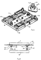
- Figure 1 is a perspective view of a frame means.
- Figure 2 is a perspective view of a carrier unit adapted to carry electrical devices, one of which is shown in exploded view.
- Figure 3 is a perspective view of a reverse side of the carrier unit of figure 2.
- Figure 4 is an enlarged portion of figure 3.
- Figure 5 is a section taken along line 5-5 of figure 2.
- Figure 6 is a section taken along line 6-6 of figure 2.
- Figure 7 is a sectional view showing the loading of a device into a carrier unit.
- Figure 8 is a partial sectional view showing the removal of a carrier unit from the frame means.
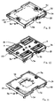
- Figure 9 is a perspective view of a standardized carrier unit perimeter.
- Figure 10 is a perspective view of a carrier unit of the kind shown in figures 1-3.
- Figure 11 is a perspective view of a carrier unit adapted for a different kind of device.
- a generally planar frame 2 with uniformly right-angled margins 3 is shown to carry a plurality of generally rectangular carrier units 4.
- the carrier units are adapted to fit into and mate with carrier unit holes 6 defined by the frame 2 and preferably arranged in rows and columns as shown.
- the frame also has identification indicia 8 on at least three viewing planes.
- the indicia comprises a computer-readable bar code in relief, in relief so that the bars do not protrude beyond the sides of the frame.
- Integral with the frame are means 10 for making the frame robotically manipulable, preferably said means comprise receptacle holes defined by the frame and adapted, for example, for use by a robotic end effector.
- the holes are disposed so as to be on the center lines of each line of carrier units.
- These holes 12 are preferably used for frame indexing by a process machine, that is, the carrier units are located and identified by the holes. This can be done by using some sort of a "walking beam” mechanism conventionally known.
- the holes 12 can also be used for frame alignment.
- the carrier unit holes 6 are generally rectangular with one corner 14 being beveled. As will be explained, said beveled corner matches and mates with a notched corner of the carrier units 4 to indicate proper orientation of the carrier units.
- FIG. 2 a more detailed showing of a carrier unit 4 is presented figure 2 being a topside view of a carrier unit 4 disposed in a frame 2 and figure 3 being an underside view of the carrier unit.
- the carrier unit as shown in these figures defines four electrical device seats 16. Each seat comprises a sleeve open at both top and bottom, the sleeves conforming to the marginal size and form of a particular type of electrical device as will be explained.
- the devices are loaded into the seats and are latched therein by a plurality of device latches 18a and 18b.
- the device latches are generally in the form of an inverted “L” with the base leg of the "L” being used to hook the device and hold it against a stop which is a seating plant or shoulder 20 intruding into the sleeve.
- a stop which is a seating plant or shoulder 20 intruding into the sleeve.
- two latches 18A hook one end of a device and two latches 18B hook an opposite end of the device, the latches operatively opposed to the stop to hold the device therebetween.
- a plurality of alignment holes 22 and 24, which are defined by sleeves protruding through a web 26, are used to precisely locate within a carrier unit the seated devices for a processing probe or marker.
- the web 26 is the interconnecting structure which ties seat walls, sleeves, and a carrier unit perimeter wall together in place.
- each carrier unit Projecting from a base of each carrier unit are four planarization posts 28. The purpose of the posts will be more fully explained later.
- the long sides of the carrier units are centrally and transversally indented to form receptacles 30 which are adapted to being gripped by a robotic end effector.
- the receptacles 30 provide a means by which the carrier units can be automatically loaded into a frame with conventional pick-and-place equipment or robots such as the Seiko RT-2000 or the IBM 7535 machines.
- An electrical device 32 having sixteen contacts or leads is shown exploded from a carrier unit seat 16 and is oriented reverse-side-up as it would be disposed within the carrier unit.
- the carrier unit is also shown to have a notched corner 34 which matches the beveled corner 14 of the frame. The matching of the notch and bevel indicate that the carrier unit is properly oriented within the frame.
- carrier unit retention latches generally designated 36.
- a plurality of resilient prongs 38 of a carrier unit retention latch 36 are uniformly and angularly spaced around an imaginary circle, each prong having an outwardly tapered barbed end 40.
- the prongs of each carrier unit retention latch are so disposed that they appear to be spaced-apart slats of an imaginary hollow cylinder and the barbed ends appear to be wedges of a conical arrowhead atop the cylinder, the cylinder inside diameter being an extension of the alignment hole 22.
- each carrier unit retention latch are adapted to radially collapse together whenever the barbed ends are inserted into a catch hole too small for the cone of the barbed ends to freely pass through.
- the taper of the barbed ends act as cams riding against the rim of the hole forcing the barbed ends of the prongs to radially move together.
- the prongs resiliently return to their spaced-apart positions if the diameter of the hole is at least equal to the outer diameter of the prong cylinder.
- the resiliency of the prongs are functions of the design length of the latch beam and the prong material's flexural modulus.
- the fact that the inside diameter of the prongs' cylinder is an extension of alignment hole 22 saves space on the carrier unit face. The extension simultaneously provides an alignment hole and clearance for the prongs to collapse together.
- each carrier unit has a pair of integral carrier unit retention latches 36 oppositely and centrally disposed proximate the short ends of the carrier unit.
- the pair of latches When loading a carrier unit into the frame, the pair of latches are forced through a corresponding pair of catch holes 44 defined by a pair of flanges 42 integral with the frame.
- the flanges are extensions of the frame which project into the carrier unit hole 16.
- the diameter of the catch holes 44 are greater than the outer diameter of the prong cylinder but less than the largest outer diameter of the cone of the barbed ends. The barbed ends prevent removal of the carrier unit without the use of a removal tool as will be described.
- the length of the prongs 38 is adapted to provide a suitable amount of carrier unit 4 travel normal to the general plane of the frame.
- the length of the prongs from a base of the carrier unit to the barbed end of the prongs is sufficiently greater than the thickness of the flanges 42 to enable the carrier units to effectively "float" on the frame.
- a frame 2 and a carrier unit 4 are shown to be disposed upon a bi-level process machine platform 48 having two reference planes.
- the frame is supported by its angled margin 3 resting upon the lower reference plane, while the amount of carrier unit travel normal to the frame is sufficient to allow the carrier unit to rest entirely on its planarization posts 28 which are resting on the upper reference plane.
- the differential between the upper and lower reference planes, the length of the planarization posts, and the amount of carrier unit travel are set so that when the frame is seated on the lower plane of the platform 48, all the carrier units are raised up slightly from the frame by the upper plane of the platform, approximately .030 inches.
- the frame could be mounted on an X-Y table and indexed under some type of insertion head containing the device to be loaded. Once a device is centered over a device seat then the insertion head pushes the device past the device retention latches, 18A and 18B, and seats it. It should be noted that the devices are totally recessed into the carrier units to virtually eliminate accidental leading bending after it is loaded.
- An alternative loading method would be to first retract the device retention latches with some latch retraction means on the insertion head, then simply drop the device. The latches would then spring back and retain the device after the insertion head is withdrawn. Unloading the devices can be accomplished by reversing the sequence in the aforementioned methods. The only differences are that the device would be pushed from the opposite side of the frame to overcome the device retention latch force, or a vacuum pick would be used to remove the devices in the alternative method.
- an insertion head having a body 68 with a facing 69 is shown in the act of inserting a first electrical device 32 into a first device seat 16 while a second device is shown already seated in a second seat.
- the insertion head has a device-holding cavity 70 open to the facing 69 into which the device-to-be-loaded is placed with the leads of the device being generally oriented inboard for proper subsequent orientation of the device in the seat 16.
- the cavity 70 is defined by the body 68 and the device is held by a vacuum means in the cavity 70 until it is released and loaded into the seat.
- the cavity 70 is defined by a pair of adjustable or biased jaws 71A and 71B and the device is ejected by releasing it and allowing it to drop.
- Projecting normally from the facing 69 are a pair of tine means 72A and 72B, each tine having a beveled end 74.
- the tines are disposed at opposite ends of the device holding cavity, the ends which correspond to the device ends which will be hooked by the device latches 18A and 18B.
- the tines are so disposed and adapted that as the facing 69 is brought to bear against the topside of the carrier unit 4 in alignment with the seat 16, the beveled tine ends act as cams against the base legs 19A and 19B of the device latches forcing the latches to retract to allow clear passage of the device between said legs and into and out of the seat, the latches 18A and 18B being resilient and their resiliency being functions of their material's flexural modulus.
- a carrier unit removal tool having a body 62 from which normally project a plurality of posts 64.
- the number and disposition of the posts 64 correspond to the number and disposition of carrier unit retention latches 36 of a carrier unit 4 being removed from a frame 2, that is, they match in number and the posts are simultaneously alignable with the latches.
- Each post defines at its free end a centered, inverted cconical hole 66.
- the posts are brought to forcibly bear against the barbed ends 40 of the latches.
- the slopes 68 and the dimensions of the conical hole 66 are adapted to partially receive and force together the barbed ends sufficiently to enable the barbed ends to be pulled though the catch holes 44, and thus releasing the carrier unit from the frame.
- a perimeter 50 common to all carrier unit variations is shown having a personality core 52 and wall 54.
- a significant advantage of this invention is that a wide range of electrical device types and forms can be handled without a variation in the basic outside perimeter and retention latches of the carrier units. It is only the personality core that changes.
- the core of figure 9 is shown in blank.
- the dashed line 52 shows generally the area of the core which is personalizable.
- carrier unit 4 is shown to illustrate that its perimeter wall 54, carrier unit retention latches 36 and planarization posts 28 are the same as those shown in figure 9. In this case, however, a personality core has been added comprising the web 26, the seats 16 and the alignment holes 24.
- a second variation 56 of a carrier unit is shown. Its perimeter, carrier unit retention latches, and planarization posts are identical to those carrier units of figures 9 and 10. Only the personality core is different. It comprises of a web 57 defining a single seat 58, and adapted to carry an electrical device packaged in a form commonly known as pin grid array (PGA).
- PGA pin grid array
- each device seat defined by a carrier unit can be open at both top and bottom so as to expose a top and a bottom side of a seated device sufficiently to eliminate any necessity for removing the device from its carrier unit during backend processing.
- a frame is set up by latching into it carrier units suitable for the form of the electrical devices which will be processed.
- the devices are then loaded into the carrier units and remain there throughout the processing.
- the frame is then transported by conveyor belt or other appropriate means to and from the steps of the processing. Access to the device can be gained both from above the frame and below.
- the devices are disposed in the carrier units "dead bug" fashion, that is, with their leads generally oriented upward. Processing machine contactors can thus make contact with each device from above the frame.
- all of the devices' leads will be in a common plane when the frame is mounted on a process platform as shown in figures 5 and 6. Thus devices may be electrically contacted singly or in multiples simultaneously.
- each frame is uniquely marked, and a device's position on the frame is constant and can be uniquely identified, processing results about each individual device can be easily and unambiguously maintained.
- the devices can be marked from either side of the frame. The devices are not unloaded until all process steps are completed, and at that point the unique identifiability of each device can be used to precisely sort them.
- the material of the carrier units preferably is selected to resist high temperature deformities, static build up and be highly resistive.
- One such material is a high temperature, graphite-loaded thermoplastic known as polyethersulfone. It contains graphite fibers to drain off any static build up that can cause electrostatic discharge damage to the devices.
- the resistivity of the material is preferably held to between 109 - 1014 ohms per square inch.
- the high temperature properties of the polyethersulfone enable the loaded frames to carry the devices throughout all heating and cooling chambers commonly known as "soak" chambers.
- the material's trade name is VICTREX manufactured by ICI Americas, Inc., Wilmington, Delaware.
- the carrier units can be non-removably affixed into the frame means by rivet or other suitable means in place of te carrier unit retention latches.
- the carrier unit retention latches can be shortened to eliminate the floating travel, or the carrier units can be otherwise affixed to the frame by bolt, rivet or other suitable means.
- the carrier units can be an integral part of the frame.
Landscapes
- Engineering & Computer Science (AREA)
- Manufacturing & Machinery (AREA)
- Microelectronics & Electronic Packaging (AREA)
- Container, Conveyance, Adherence, Positioning, Of Wafer (AREA)
- Packaging Frangible Articles (AREA)
- Control Of Vending Devices And Auxiliary Devices For Vending Devices (AREA)
- Types And Forms Of Lifts (AREA)
- Electrical Discharge Machining, Electrochemical Machining, And Combined Machining (AREA)
- Feeding Of Articles To Conveyors (AREA)
- Automatic Assembly (AREA)
- Packages (AREA)
- Packaging Of Annular Or Rod-Shaped Articles, Wearing Apparel, Cassettes, Or The Like (AREA)
Claims (9)
- Moyen de transport pour le transport en cours de traitement de dispositifs électriques comportant :a) un ensemble d'unités porteuses (4;56) pour porter au moins un dispositif électrique (32), chacun de telle sorte que le dessus et le dessous de chaque dispositif électrique porté (32) est exposé pour permettre son traitement alors qu'il se trouve porté dans son unité porteuse correspondante ; etb) un moyen formant châssis (2) susceptible de porter les unités porteuses (4;56) les unes avec les autres dans sensiblement le même plan pendant le traitement, caractérisé en ce que :c) le moyen formant châssis (2) est une feuille généralement plane,d) les unités porteuses (4;56) sont supportées en relation fixe dans le plan de cette relation dans le même plan par des moyens (36,44) fixant chaque unité porteuse (4;56) dans un orifice correspondant d'unités porteuses (6) défini par le moyen formant châssis (2),e) les moyens (36,44) servant à fixer chaque unité porteuse (4;56) dans son orifice d'unité porteuse correspondant (6) est susceptible de permettre à l'unité porteuse (4;56) de flotter perpendiculairement par rapport au plan du moyen formant châssis (2),f) un ensemble de piliers de planarisation (28) font saillie par rapport à une base de chaque unité porteuse (4;56), etg) le moyen de transport comporte en outre un moyen support de châssis (3) susceptible de reposer sur un niveau inférieur d'une plate-forme de traitement à deux niveaux (48) et sert à espacer le moyen formant châssis (2) au dessus du niveau supérieur de la plate-forme (48) d'une quantité selon laquelle les unités porteuses (4;56) fixées dans ledit moyen formant châssis (2) reposent totalement sur leurs piliers de planarisation correspondants (28) lesquels reposent au niveau supérieur de la plate-forme (48).
- Moyen de transport selon la revendication 1, dans lequel les piliers de planarisation (28) agissent également en tant que moyens pour exposer le dessus et le dessous de chaque dispositif électrique (32) porté par chacune des unités porteuses (4;56).
- Moyen de transport selon la revendication 1 ou 2, dans lequel le moyen (2) pour maintenir les unités porteuses (4;56) supporte les unités porteuses de sorte qu'elles soient uniformément orientées.
- Moyen de transport selon les revendications 1, 2 ou 3, dans lequel le moyen (2) pour maintenir les unités porteuses comporte :a) le moyen formant châssis (2),b) un ensemble d'orifices se trouvant de façon générale dans le même plan (6) définis par le moyen formant châssis (2) dans lesquels les unités porteuses (4;56) sont disposées, etc) des moyens (38,40) pour fixer les unités porteuses (4;56) dans leurs orifices respectifs (6) mais permettant aux unités porteuses (4;56) de flotter par rapport au plan de leurs orifices (6).
- Moyen de transport selon la revendication 4, dans lequel les moyens (38,40) pour fixer les unités porteuses (4;56) dans leurs orifices respectifs (6) comportent :a) un ensemble de moyens formant fourches (38) faisant saillie à partir d'une base de chacune des unités porteuses (4;56), chaque moyen formant fourche (38) comportant une extrémité fourchue élastique et susceptible d'être repliée radialement (40), etb) un ensemble d'orifices d'accrochage correspondants (44) définis par le moyen formant châssis (2), la dimension de chaque orifice d'accrochage (44) étant inférieure aux dimensions d'une extrémité fourchue qui n'est pas repliée (40) d'un moyen formant fourche correspondant (38) mais étant suffisamment grande pour permettre le passage au travers de l'extrémité fourchue rabattue de telle sorte que les extrémités fourchues soient saisies lorsque le moyen formant fourche est inséré à l'intérieur de l'orifice d'accrochage (44).
- Moyen de transport selon l'une quelconque des revendications précédentes, dans lequel chaque unité porteuse (4;56) comporte en outre :a) un périmètre (54) qui est du même type que les périmètres des autres unités porteuses, etb) un noyau (52) qui est spécialement conçu pour des dimensions et formes d'un dispositif électrique particulier.
- Moyen de transport selon la revendication 6, dans lequel le noyau (26;57) comporte en outre :a) un ou plusieurs sièges de dispositifs électriques (16;58) dans lesquels les dispositifs électriques (32) sont logés,b) des moyens pour aligner une sonde de traitement avec les dispositifs électriques logés dans l'unité porteuse, etc) une bordure fixée au périmètre de l'unité porteuse (54) pour maintenir le(s) siège(s) de dispositifs (16;58) et le moyen pour aligner une sonde de traitement en position fixe par rapport au noyau (52), l'ensemble des sièges de dispositifs étant fixé de façon à se trouver dans le même plan.
- Moyen de transport selon la revendication 7, dans lequel chaque siège de dispositif électrique (16;58) comporte :a) un fourreau formant siège qui correspond à une dimension et une forme marginale d'un dispositif électrique (32) qui est susceptible de se loger dans celui-ci,b) un moyen d'arrêt (20) pénétrant à l'intérieur du fourreau formant siège pour limiter la profondeur selon laquelle le dispositif électrique (32) est logé, etc) un ensemble de moyens formant crochets susceptibles de se rétracter élastiquement (18a,18b) opposés opérationnellement par rapport au moyen d'arrêt (20) pour saisir le dispositif électrique (32) entre eux.
- Moyen de transport selon la revendication 4, dans lequel les orifices d'unités porteuses (6) sont disposés selon des coordonnées pour permettre aux unités porteuses qui y sont disposées d'être identifiables sans erreur par un ensemble de coordonnées et de plus comportent un moyen d'indexation de châssis (12) destiné à être utilisé par une machine de traitement pour localiser chaque unité porteuse individuelle en fonction de ses coordonnées.
Priority Applications (1)
| Application Number | Priority Date | Filing Date | Title |
|---|---|---|---|
| AT87903803T ATE100268T1 (de) | 1986-06-27 | 1987-05-27 | Transportvorrichtung fuer elektrische gegenstaende. |
Applications Claiming Priority (2)
| Application Number | Priority Date | Filing Date | Title |
|---|---|---|---|
| US87930786A | 1986-06-27 | 1986-06-27 | |
| US879307 | 1986-06-27 |
Publications (3)
| Publication Number | Publication Date |
|---|---|
| EP0271533A1 EP0271533A1 (fr) | 1988-06-22 |
| EP0271533A4 EP0271533A4 (fr) | 1989-08-09 |
| EP0271533B1 true EP0271533B1 (fr) | 1994-01-12 |
Family
ID=25373873
Family Applications (1)
| Application Number | Title | Priority Date | Filing Date |
|---|---|---|---|
| EP87903803A Expired - Lifetime EP0271533B1 (fr) | 1986-06-27 | 1987-05-27 | Moyen de transport pour dispositifs electriques |
Country Status (7)
| Country | Link |
|---|---|
| EP (1) | EP0271533B1 (fr) |
| JP (1) | JP2631677B2 (fr) |
| KR (1) | KR950007247B1 (fr) |
| AT (1) | ATE100268T1 (fr) |
| AU (1) | AU7489287A (fr) |
| DE (1) | DE3788789D1 (fr) |
| WO (1) | WO1988000161A1 (fr) |
Families Citing this family (4)
| Publication number | Priority date | Publication date | Assignee | Title |
|---|---|---|---|---|
| US5203454A (en) * | 1990-10-25 | 1993-04-20 | Strong Leslie G | Method and apparatus for transporting sensitive electronic components |
| US5407068A (en) * | 1991-10-22 | 1995-04-18 | Strong; Leslie G. | Method and apparatus for transporting test boards |
| US10976498B2 (en) | 2019-06-14 | 2021-04-13 | Cisco Technology, Inc. | Tray and clip structure for optomechanical components |
| CN115838024A (zh) * | 2022-11-30 | 2023-03-24 | 苏州中集良才物流科技股份有限公司 | 一种带有防脱落滑动限位机构的托盘 |
Family Cites Families (14)
| Publication number | Priority date | Publication date | Assignee | Title |
|---|---|---|---|---|
| US3444993A (en) * | 1968-04-23 | 1969-05-20 | Thomas J Lunsford | Component package with dust cover |
| US3673543A (en) * | 1970-04-27 | 1972-06-27 | Thomas & Betts Corp | Micro-circuit pack receptacle |
| US3809233A (en) * | 1971-02-03 | 1974-05-07 | Western Electric Co | Method of and package for transporting articles |
| JPS5028659B2 (fr) * | 1971-10-19 | 1975-09-17 | ||
| US3772573A (en) * | 1972-07-05 | 1973-11-13 | Burroughs Corp | Molded pallet |
| US3946864A (en) * | 1974-07-01 | 1976-03-30 | Hutson Jearld L | Semiconductor chip package |
| US4012608A (en) * | 1974-08-20 | 1977-03-15 | Amp Incorporated | Miniature switch with substantial wiping action |
| US4015707A (en) * | 1976-06-07 | 1977-04-05 | Rca Corporation | Carrier for semiconductor components |
| JPS5937800B2 (ja) * | 1978-03-01 | 1984-09-12 | シチズン時計株式会社 | デジタル電子時計 |
| US4210243A (en) * | 1978-12-26 | 1980-07-01 | Gte Automatic Electric Laboratories, Inc. | Tray for holding components with preformed leads |
| DE2929716A1 (de) * | 1979-07-21 | 1981-02-12 | Philips Patentverwaltung | Verpackung zur aufnahme einer vielzahl von plaettchenfoermigen teilen |
| US4657137A (en) * | 1981-05-22 | 1987-04-14 | North American Philips Corporation | Multi-chip packaging system |
| US4442938A (en) * | 1983-03-22 | 1984-04-17 | Advanced Interconnections | Socket terminal positioning method and construction |
| US4483442A (en) * | 1983-11-18 | 1984-11-20 | Continental-Wirt Electronics Corp. | Packing tray for flat cable conductors having latchable covers |
-
1987
- 1987-05-27 AU AU74892/87A patent/AU7489287A/en not_active Abandoned
- 1987-05-27 WO PCT/US1987/001245 patent/WO1988000161A1/fr not_active Ceased
- 1987-05-27 EP EP87903803A patent/EP0271533B1/fr not_active Expired - Lifetime
- 1987-05-27 JP JP62503410A patent/JP2631677B2/ja not_active Expired - Fee Related
- 1987-05-27 AT AT87903803T patent/ATE100268T1/de not_active IP Right Cessation
- 1987-05-27 KR KR1019880700217A patent/KR950007247B1/ko not_active Expired - Fee Related
- 1987-05-27 DE DE87903803T patent/DE3788789D1/de not_active Expired - Lifetime
Non-Patent Citations (2)
| Title |
|---|
| IBM TECHNICAL DISCLOSURE BULLETIN, vol. 17, no. 6, November 1974, pages 1629-1630 ; New York, US; J.C. FORMICHELLI et al.: "Pallets for handling modules of various sizes" * |
| IBM TECHNICAL DISCLOSURE BULLETIN, vol. 25, no. 11b, April 1983, pages 6123-6125 ; New York, US; H.R. POWELEIT et al.: "MLC substrate holding fixture" * |
Also Published As
| Publication number | Publication date |
|---|---|
| KR880701204A (ko) | 1988-07-26 |
| ATE100268T1 (de) | 1994-01-15 |
| KR950007247B1 (ko) | 1995-07-07 |
| EP0271533A4 (fr) | 1989-08-09 |
| JP2631677B2 (ja) | 1997-07-16 |
| AU7489287A (en) | 1988-01-29 |
| WO1988000161A1 (fr) | 1988-01-14 |
| EP0271533A1 (fr) | 1988-06-22 |
| JPH01500506A (ja) | 1989-02-23 |
| DE3788789D1 (de) | 1994-02-24 |
Similar Documents
| Publication | Publication Date | Title |
|---|---|---|
| US5131535A (en) | Electrical device transport medium | |
| JP3951436B2 (ja) | Ic試験装置 | |
| DE19680785B4 (de) | Halbleiterbauelement-Testgerät und Halbleiterbauelement-Testsystem, das eine Mehrzahl von Halbleiterbauelement-Testgeräten enthält | |
| JPH0943309A (ja) | Ic試験装置 | |
| JP3136613B2 (ja) | 半導体デバイス試験装置及びこの試験装置に使用されるテストトレイ | |
| EP0412945B1 (fr) | Manipulation automatique de magasins différents à l'aide de moyens de préhension et de codes d'identification standardisés | |
| US6304073B1 (en) | IC testing apparatus | |
| US8453841B1 (en) | Disk placement and storage assembly with disk cassette and disk slotter | |
| US6474475B1 (en) | Apparatus for handling stacked integrated circuit devices | |
| US5180974A (en) | Semiconductor testing and shipping system | |
| US5636745A (en) | Tray for a component and an apparatus for accurately placing a component within the tray | |
| JPH10291645A (ja) | Ic用トレイ取出装置及びic用トレイ収納装置 | |
| JP3376784B2 (ja) | Ic試験装置 | |
| JP4222442B2 (ja) | 電子部品試験装置用インサート | |
| EP0271533B1 (fr) | Moyen de transport pour dispositifs electriques | |
| JPH112657A (ja) | 複合ic試験装置 | |
| JP2940858B2 (ja) | Ic試験装置 | |
| US5565008A (en) | Process of raising a semiconductor device out of a pallet using a positioning rod | |
| KR19980071417A (ko) | 반도체 디바이스 시험장치 | |
| JP3379077B2 (ja) | Ic試験装置 | |
| US20030020457A1 (en) | Test handler apparatus for SMD (surface mount devices), BGA (ball grid arrays) and CSP (chip scale packages) | |
| US7810645B2 (en) | Paddle for securely mounting a wafer cassette holder thereto | |
| JP2007024907A (ja) | Ic試験システム | |
| US6257933B1 (en) | Connector | |
| KR19990059041A (ko) | 반도체패키지 제조용 마킹 장치 |
Legal Events
| Date | Code | Title | Description |
|---|---|---|---|
| PUAI | Public reference made under article 153(3) epc to a published international application that has entered the european phase |
Free format text: ORIGINAL CODE: 0009012 |
|
| 17P | Request for examination filed |
Effective date: 19880307 |
|
| AK | Designated contracting states |
Kind code of ref document: A1 Designated state(s): AT BE CH DE FR GB IT LI LU NL SE |
|
| A4 | Supplementary search report drawn up and despatched |
Effective date: 19890809 |
|
| 17Q | First examination report despatched |
Effective date: 19910703 |
|
| GRAA | (expected) grant |
Free format text: ORIGINAL CODE: 0009210 |
|
| AK | Designated contracting states |
Kind code of ref document: B1 Designated state(s): AT BE CH DE FR GB IT LI LU NL SE |
|
| PG25 | Lapsed in a contracting state [announced via postgrant information from national office to epo] |
Ref country code: IT Free format text: LAPSE BECAUSE OF FAILURE TO SUBMIT A TRANSLATION OF THE DESCRIPTION OR TO PAY THE FEE WITHIN THE PRESCRIBED TIME-LIMIT;WARNING: LAPSES OF ITALIAN PATENTS WITH EFFECTIVE DATE BEFORE 2007 MAY HAVE OCCURRED AT ANY TIME BEFORE 2007. THE CORRECT EFFECTIVE DATE MAY BE DIFFERENT FROM THE ONE RECORDED. Effective date: 19940112 Ref country code: CH Effective date: 19940112 Ref country code: SE Effective date: 19940112 Ref country code: NL Effective date: 19940112 Ref country code: AT Effective date: 19940112 Ref country code: DE Effective date: 19940112 Ref country code: LI Effective date: 19940112 Ref country code: BE Effective date: 19940112 Ref country code: FR Effective date: 19940112 |
|
| REF | Corresponds to: |
Ref document number: 100268 Country of ref document: AT Date of ref document: 19940115 Kind code of ref document: T |
|
| REF | Corresponds to: |
Ref document number: 3788789 Country of ref document: DE Date of ref document: 19940224 |
|
| REG | Reference to a national code |
Ref country code: CH Ref legal event code: PL |
|
| PG25 | Lapsed in a contracting state [announced via postgrant information from national office to epo] |
Ref country code: GB Effective date: 19940527 |
|
| PG25 | Lapsed in a contracting state [announced via postgrant information from national office to epo] |
Ref country code: LU Free format text: LAPSE BECAUSE OF NON-PAYMENT OF DUE FEES Effective date: 19940531 |
|
| EN | Fr: translation not filed | ||
| NLV1 | Nl: lapsed or annulled due to failure to fulfill the requirements of art. 29p and 29m of the patents act | ||
| PLBE | No opposition filed within time limit |
Free format text: ORIGINAL CODE: 0009261 |
|
| 26N | No opposition filed | ||
| GBPC | Gb: european patent ceased through non-payment of renewal fee |
Effective date: 19940527 |