EP0271846B1 - Système et circuit de traitement d'un signal de télévision - Google Patents
Système et circuit de traitement d'un signal de télévision Download PDFInfo
- Publication number
- EP0271846B1 EP0271846B1 EP87118427A EP87118427A EP0271846B1 EP 0271846 B1 EP0271846 B1 EP 0271846B1 EP 87118427 A EP87118427 A EP 87118427A EP 87118427 A EP87118427 A EP 87118427A EP 0271846 B1 EP0271846 B1 EP 0271846B1
- Authority
- EP
- European Patent Office
- Prior art keywords
- signals
- frequency
- signal
- registers
- variable
- Prior art date
- Legal status (The legal status is an assumption and is not a legal conclusion. Google has not performed a legal analysis and makes no representation as to the accuracy of the status listed.)
- Expired - Lifetime
Links
Images

Classifications
-
- H—ELECTRICITY
- H04—ELECTRIC COMMUNICATION TECHNIQUE
- H04N—PICTORIAL COMMUNICATION, e.g. TELEVISION
- H04N11/00—Colour television systems
- H04N11/04—Colour television systems using pulse code modulation
- H04N11/042—Codec means
- H04N11/044—Codec means involving transform coding
-
- H—ELECTRICITY
- H04—ELECTRIC COMMUNICATION TECHNIQUE
- H04N—PICTORIAL COMMUNICATION, e.g. TELEVISION
- H04N19/00—Methods or arrangements for coding, decoding, compressing or decompressing digital video signals
Definitions
- Colour television signals e.g. PAL or NTSC
- Colour television signals are generally unsuitable for encoding through unidimensional or bidimensional high efficiency transform.
- signals y, c1, c2 are constant, which does not occur for signal s(t) because modulation introduces an alternating current component.
- the problem may be solved by inserting a demodulator between the signal source and the converter.
- compression efficiency improves, but the signal quality considerably degrades, while costs increase due to the demodulation and remodulation circuitry.
- This invention provides a method for processing composite colour television signals having amplitude modulation encoded chrominance information comprising chrominance signals c1 and c2 and a baseband component comprising a luminance signal y , said method permitting the encoding of said colour television signals through a unidimensional or bidimensional transform, said method being characterized by the following steps:
- US-A 4 541 008 discloses the use of a component separation for the sampled digital values of the signal. The coding is performed separately for each single component. This known method has at least three drawbacks:
- Signals are coded and decoded several times. The quality of the signal will degrade.
- US-A 4 541 008 takes the radio signal of the NTSC norm US-A 4 541 008 the radio signal of the NTSC norm and separates or demodulates it obtaining Y, I and Q. In the present method, however, a demodulation or separation is not involved and is not a demodulation as demonstrated by the fact that the same equations are utilized for NTSC signals a well as for PAL video signals.
- the system of US-A 4 541 008 is only able to receive NTSC. To receive a PAL signal said system mustchange the receiver. The method of the present system is able to receive any video signal (NTSC, PAL, etc.) and does not need to change the receiver when changing signals.
- the present method basically will separate the “Low Frequency Signal Components (LFSC)” from the “High Frequency Signal components (HFSC)” and further separating the HFSC into two signals, of which one is in quadrature to the other. This separation is performed without enganging the colour subcarrier phase.
- LFSC Low Frequency Signal Components
- HFSC High Frequency Signal components
- Fig. 1 shows the block diagram of the processing system where an analog signal (SAI) is applied to block 1, which, according to the invention, consists of a variable clock generator and an analog to digital converter, the output of which feeds a digital processor PRO which in turn supplies three processed signals py, pc1, pc2 to block 3, which is a "Redundancy Reducing System".
- SAI analog signal
- block 1 which, according to the invention, consists of a variable clock generator and an analog to digital converter, the output of which feeds a digital processor PRO which in turn supplies three processed signals py, pc1, pc2 to block 3, which is a "Redundancy Reducing System".
- the processing system of the invention consists of two parts:
- sampling clock ck(t) of the analog input signal SAI must respect two prime bonds or conditions:
- a general solution satisfying above bonds a) and b) consists in adopting two different sampling frequencies, one for the active part of the video signal and one for the line synchronism part, complying with Nyquist's criterion on the single portions of the composite signal.
- PAL signal can be taken as an example (see figures 2a and 2b).
- the PAL signal is sampled with variable frequency clock ck(t) (obtained from the circuit of Fig. 2b) as a function of the signal spectrum content: in the active area, where the spectrum contains more energy sampling signal ck(t) reaches the maximum frequency ckmax.
- Clock master C (see Fig. 2b) has e.g. frequency 2270xFh.
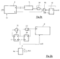
- Variable frequency sampling clock ck(t) is generated by said circuit of Fig. 2b containing a control signal generator 12 (see Fig. 2a) and a sequential network consisting of flip-flop 3A and 3B, NAND gate 3C and OR gate 3D, which together generate a variable frequency clock signal ck(t), dividing in this case input frequency C by two or by three.
- Control circuit 12 of Fig. 2b is shown in detail in Fig. 2a. It consists of counter 4, decoder 5, flip-flop 6C and gates 6A and 6B.
- Circuit 12 is slave of external signal ES in phase relationship with the TV synchronisms.
- control signal CO is produced at the output of 6C.
- Fig. 2a which consists of counter modulus 1120 (block 4), decoder 5 generating a pulse the duration of which equals one clock stroke when counter 4 reaches "30", two gates 6A and 6B and flip-flop 6C.
- s(KT) y(KT)+u(KT) ⁇ cos[K ⁇ 1 ⁇ 2 ⁇ +K ⁇ 2 ⁇ /(1135 ⁇ 625)]+ v(KT) ⁇ sin[K ⁇ 1 ⁇ 2 ⁇ +K ⁇ 2 ⁇ /(1135 ⁇ 625)
- the arithmetic operations permit to obtain, e.g. still in the case where system input signal SAI of Fig. 1 is PAL the signals py, pc1, pc2 from 3).
- py signals are proportional to the mean value of signal (y(t)), pc signals define the amplitude and phase of the alternating current component.
- py Since py is proportional to mean signal y(t) it has the same spectrum characteristics of luminance as the component signal, less an aliasing chrominance error.
- Signals pc1, pc2 have spectrum characteristics which are linearly dependent on the hrominance components of the component signal (u,v in case of PAL) vs sampling with respect tc the coloured subcarrier.
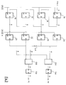
- the PRO circuit shown in the block diagram of Fig. 3, consists of four cascaded 8-bit registers 1A, 1B, 1C and 1D, other four 8-bit registers 2A, 2B, 2C and 2D each one of which is parallel connected to one of registers 1, eight inverters I1 to I8, two 8-bit adders 13A and 13B and two 9-bit registers 5A and 5B at the output.
- the NTSC signal processing procedure is similar to the one for the PAL signal.
- the difference lies in clock master frequency C, which is 1820xFh.MHz and in the number of clock strokes at one half and one third frequency, viz. 868 and 28, respectively.
- the first phenomenon mutually exchanges the significance of output signals pc1 and pc2. This can be remedied by changing the sequence in which they are sent to the transformer.
- the second phenomenon generates a vertical axis modulation, the effects of which can only be attenuated by multiplying -1 time signals pc1 and pc2 on a part of the lines, i.e. pc1 and pc2 are unaltered on lines 1, 2, inverted on lines 3, 4 and become again unaltered on lines 5, 6 etc.
- phase rotation from one line to the other is 180° and is compensated by multiplying -1 time signals pc1 and pc2 on alternating lines.
Landscapes
- Engineering & Computer Science (AREA)
- Multimedia (AREA)
- Signal Processing (AREA)
- Color Television Systems (AREA)
- Processing Of Color Television Signals (AREA)
- Radio Transmission System (AREA)
- Picture Signal Circuits (AREA)
- Selective Calling Equipment (AREA)
Claims (5)
- Procédé de traitement de signaux composites de télévision en couleur présentant une information de chrominance codée par modulation d'amplitude comprenant des signaux de chrominance c1 et c2 et une composante de bande de base comprenant un signal de luminance y, ledit procédé permettant le codage desdits signaux de télévision en couleur par l'intermédiaire d'une transformée unidimensionnelle ou bi-dimensionnelle ledit procédé étant caractérisé par les étapes suivantes:(a) conversion analogique vers numérique et production d'échantillons dudit signal composite de télévision en couleur en relation avec une horloge d'échantillonnage à fréquence variable [(fréquence ck(t))],(b) choix d'une fréquence d'échantillonnage variable [ck(t)] de l'horloge pour le signal composite de télévision en couleur (SAI), de façon à obtenir un nombre d'échantillons (sn) par lignes de télévision qui soit un multiple de la dimension de la transformée;(c) transformation de façon périodique des échantillons par des opérations arithmétiques, les convertissant par ce moyen en un second signal de luminance py et pseudo-signaux de chrominance pc1 et pc2 qui sont corrélés avec lesdits signaux composites y, c1 et c2, mais sont par ailleurs différents de ceux-ci.
- Procédé selon la revendication 1, caractérisé en ce que le signal de télévision en couleur (SAI) à traiter consiste en une composante de bande de base et une composante de bande réduite, ladite composante de bande réduite étant obtenue par le codage en modulation d'amplitude de l'un ou de plusieurs desdits signaux de bande de base, dans lequel trois signaux de bande de base sont obtenus par échantillonnage à une fréquence correspondant à N fois la fréquence porteuse, suivi par addition et soustraction des échantillons.
- Procédé selon la revendication 2, caractérisé en ce que la fréquence d'échantillonnage variable [ck(t)] est toujours supérieure au double de la largeur de bande du signal de télévision en couleur.
- Procédé selon la revendication 3,caractérisé en ce que la fréquence d'échantillonnage variable [ck(t)] de ladite horloge à fréquence variable dispose de seulement deux valeurs pré-établies.
- Circuit conçu pour la mise en oeuvre du procédé selon l'une au moins des revendications 1 à 4, comprenant au moins un générateur d'horloge variable (1) et un convertisseur analogique vers numérique, et un processeur numérique (PRO) consistant en:(I) quatre registres en cascade (1A, B, C, D),(II) quatre autres registres (2A, B, C, D), chacun étant relié en parallèle à l'un desdits quatre registres en cascade,(III) huit inverseurs (I1 à I8) reliés à deux desdits autres registres,(IV) deux circuits d'addition (13A, 13B), l'un desdits deux circuits d'addition étant reliés directement à l'ensemble desdits quatres autres registres, l'autre desdits circuits d'addition étant reliés directement à deux desdits autres registres et auxdits huit inverseurs vers les deux autres desdits autres registres, et(V) deux registres de sortie (5A, 5B) relié chacun à l'un desdits deux circuits d'addition.
Applications Claiming Priority (2)
| Application Number | Priority Date | Filing Date | Title |
|---|---|---|---|
| IT2271786 | 1986-12-17 | ||
| IT22717/86A IT1199794B (it) | 1986-12-17 | 1986-12-17 | Sistema e circuiti per l'elaborazione di segnale televisivo |
Publications (3)
| Publication Number | Publication Date |
|---|---|
| EP0271846A2 EP0271846A2 (fr) | 1988-06-22 |
| EP0271846A3 EP0271846A3 (en) | 1989-07-19 |
| EP0271846B1 true EP0271846B1 (fr) | 1995-04-05 |
Family
ID=11199600
Family Applications (1)
| Application Number | Title | Priority Date | Filing Date |
|---|---|---|---|
| EP87118427A Expired - Lifetime EP0271846B1 (fr) | 1986-12-17 | 1987-12-12 | Système et circuit de traitement d'un signal de télévision |
Country Status (11)
| Country | Link |
|---|---|
| US (1) | US4894710A (fr) |
| EP (1) | EP0271846B1 (fr) |
| CN (1) | CN87108133A (fr) |
| AT (1) | ATE120917T1 (fr) |
| BR (1) | BR8706872A (fr) |
| CA (1) | CA1281127C (fr) |
| DE (1) | DE3751222T2 (fr) |
| ES (1) | ES2070816T3 (fr) |
| IT (1) | IT1199794B (fr) |
| MX (1) | MX168855B (fr) |
| NO (1) | NO875153L (fr) |
Family Cites Families (12)
| Publication number | Priority date | Publication date | Assignee | Title |
|---|---|---|---|---|
| US3071727A (en) * | 1961-05-08 | 1963-01-01 | Bell Telephone Labor Inc | Bandwidth reduction system |
| JPS5412369B2 (fr) * | 1975-02-28 | 1979-05-22 | ||
| US4129882A (en) * | 1977-05-06 | 1978-12-12 | Bell Telephone Laboratories, Incorporated | Video coder for color signals |
| US4106053A (en) * | 1977-08-01 | 1978-08-08 | Rca Corporation | Digital sampling rate conversion of color TV signal |
| US4302775A (en) * | 1978-12-15 | 1981-11-24 | Compression Labs, Inc. | Digital video compression system and methods utilizing scene adaptive coding with rate buffer feedback |
| US4394774A (en) * | 1978-12-15 | 1983-07-19 | Compression Labs, Inc. | Digital video compression system and methods utilizing scene adaptive coding with rate buffer feedback |
| ATE45258T1 (de) * | 1981-04-10 | 1989-08-15 | Ampex | Geraet zur raeumlichen transformation von bildern. |
| US4568912A (en) * | 1982-03-18 | 1986-02-04 | Victor Company Of Japan, Limited | Method and system for translating digital signal sampled at variable frequency |
| US4589020A (en) * | 1982-11-22 | 1986-05-13 | Olympus Optical Co., Ltd. | TV video data input apparatus |
| US4541008A (en) * | 1982-12-27 | 1985-09-10 | Jones Futura Foundation, Ltd. | Television signal bandwidth reduction using variable rate transmission |
| US4695874A (en) * | 1985-11-01 | 1987-09-22 | Eastman Kodak Company | Apparatus for processing a time-division multiplex video signal having signal durations divisible by the same number |
| US4745473A (en) * | 1986-03-24 | 1988-05-17 | Harris Corporation | Hybrid image compression system |
-
1986
- 1986-12-17 IT IT22717/86A patent/IT1199794B/it active
-
1987
- 1987-12-10 NO NO875153A patent/NO875153L/no unknown
- 1987-12-11 MX MX009711A patent/MX168855B/es unknown
- 1987-12-12 ES ES87118427T patent/ES2070816T3/es not_active Expired - Lifetime
- 1987-12-12 DE DE3751222T patent/DE3751222T2/de not_active Expired - Lifetime
- 1987-12-12 EP EP87118427A patent/EP0271846B1/fr not_active Expired - Lifetime
- 1987-12-12 AT AT87118427T patent/ATE120917T1/de not_active IP Right Cessation
- 1987-12-14 US US07/132,428 patent/US4894710A/en not_active Expired - Lifetime
- 1987-12-17 CA CA000554740A patent/CA1281127C/fr not_active Expired - Lifetime
- 1987-12-17 CN CN87108133A patent/CN87108133A/zh active Pending
- 1987-12-17 BR BR8706872A patent/BR8706872A/pt not_active IP Right Cessation
Also Published As
| Publication number | Publication date |
|---|---|
| ES2070816T3 (es) | 1995-06-16 |
| MX168855B (es) | 1993-06-11 |
| IT1199794B (it) | 1988-12-30 |
| DE3751222D1 (de) | 1995-05-11 |
| DE3751222T2 (de) | 1995-09-28 |
| EP0271846A3 (en) | 1989-07-19 |
| IT8622717A0 (it) | 1986-12-17 |
| NO875153D0 (no) | 1987-12-10 |
| EP0271846A2 (fr) | 1988-06-22 |
| CN87108133A (zh) | 1988-07-06 |
| CA1281127C (fr) | 1991-03-05 |
| US4894710A (en) | 1990-01-16 |
| NO875153L (no) | 1988-06-20 |
| ATE120917T1 (de) | 1995-04-15 |
| BR8706872A (pt) | 1988-07-26 |
Similar Documents
| Publication | Publication Date | Title |
|---|---|---|
| EP0204450B1 (fr) | Système de transmission à bande passante étroite | |
| EP0336669B1 (fr) | Convertisseur de fréquence d'échantillonnage | |
| US3946432A (en) | Apparatus for digitally encoding a television signal | |
| EP0690621B1 (fr) | Convertisseur de fréquence d'échantillonnage et méthode de conversion de fréquence d'échantillonnage | |
| KR970000760B1 (ko) | 고선명도 텔레비젼 | |
| GB2186150A (en) | Bandwidth reduction and conversion of a progressive scan television signal using sum and difference components | |
| KR910004290B1 (ko) | 복합 텔레비젼 신호의 신호분리회로 | |
| US4561012A (en) | Pre-emphasis and de-emphasis filters for a composite NTSC format video signal | |
| US4054909A (en) | Method and system for bandwidth-compressed transmission of a video signal in the NTSC system | |
| CA1074436A (fr) | Dispositif de codage et/ou de decodage des signaux de television en couleur, y compris les signaux de luminance et de chrominance | |
| JPS59501529A (ja) | デ−タ周波数を低減した信号分離装置 | |
| US3891994A (en) | Colour television | |
| EP0078052A2 (fr) | Dispositif de traitement numérique de signal vidéo PAL | |
| EP0271846B1 (fr) | Système et circuit de traitement d'un signal de télévision | |
| JPH05502775A (ja) | テレビジョン信号を復号する方法 | |
| CA1161158A (fr) | Systeme numerique de transmission de signaux de television utilisant l'inversion de la chrominance | |
| US4527188A (en) | Apparatus for demodulating sampled data chroma signals | |
| US5528306A (en) | Video signal processing circuit for converting digital color difference signals into a carrier chrominance signal | |
| US4630294A (en) | Digital sample rate reduction system | |
| US5153724A (en) | Video signal switching circuit especially suitable for high definition television receiving | |
| US5621472A (en) | System for inexpensive phase coherent subcarrier generation | |
| JP2788733B2 (ja) | カラーテレビ信号処理方法及びその回路 | |
| JPH038156B2 (fr) | ||
| KR0172486B1 (ko) | 샘플링율 변환방법 및 그 장치 | |
| US4137549A (en) | DPCM Coding apparatus |
Legal Events
| Date | Code | Title | Description |
|---|---|---|---|
| PUAI | Public reference made under article 153(3) epc to a published international application that has entered the european phase |
Free format text: ORIGINAL CODE: 0009012 |
|
| AK | Designated contracting states |
Kind code of ref document: A2 Designated state(s): AT BE CH DE ES FR GB LI NL SE |
|
| PUAL | Search report despatched |
Free format text: ORIGINAL CODE: 0009013 |
|
| AK | Designated contracting states |
Kind code of ref document: A3 Designated state(s): AT BE CH DE ES FR GB LI NL SE |
|
| 17P | Request for examination filed |
Effective date: 19890921 |
|
| 17Q | First examination report despatched |
Effective date: 19920624 |
|
| RAP1 | Party data changed (applicant data changed or rights of an application transferred) |
Owner name: ALCATEL ITALIA SOCIETA PER AZIONI |
|
| GRAA | (expected) grant |
Free format text: ORIGINAL CODE: 0009210 |
|
| AK | Designated contracting states |
Kind code of ref document: B1 Designated state(s): AT BE CH DE ES FR GB LI NL SE |
|
| REF | Corresponds to: |
Ref document number: 120917 Country of ref document: AT Date of ref document: 19950415 Kind code of ref document: T |
|
| REF | Corresponds to: |
Ref document number: 3751222 Country of ref document: DE Date of ref document: 19950511 |
|
| REG | Reference to a national code |
Ref country code: ES Ref legal event code: FG2A Ref document number: 2070816 Country of ref document: ES Kind code of ref document: T3 |
|
| ET | Fr: translation filed | ||
| PLBE | No opposition filed within time limit |
Free format text: ORIGINAL CODE: 0009261 |
|
| STAA | Information on the status of an ep patent application or granted ep patent |
Free format text: STATUS: NO OPPOSITION FILED WITHIN TIME LIMIT |
|
| 26N | No opposition filed | ||
| PGFP | Annual fee paid to national office [announced via postgrant information from national office to epo] |
Ref country code: CH Payment date: 19991115 Year of fee payment: 13 |
|
| PGFP | Annual fee paid to national office [announced via postgrant information from national office to epo] |
Ref country code: NL Payment date: 19991122 Year of fee payment: 13 |
|
| PGFP | Annual fee paid to national office [announced via postgrant information from national office to epo] |
Ref country code: AT Payment date: 19991124 Year of fee payment: 13 |
|
| PGFP | Annual fee paid to national office [announced via postgrant information from national office to epo] |
Ref country code: BE Payment date: 19991216 Year of fee payment: 13 |
|
| EUG | Se: european patent has lapsed | ||
| PG25 | Lapsed in a contracting state [announced via postgrant information from national office to epo] |
Ref country code: AT Free format text: LAPSE BECAUSE OF NON-PAYMENT OF DUE FEES Effective date: 20001212 |
|
| PG25 | Lapsed in a contracting state [announced via postgrant information from national office to epo] |
Ref country code: BE Free format text: LAPSE BECAUSE OF NON-PAYMENT OF DUE FEES Effective date: 20001231 Ref country code: LI Free format text: LAPSE BECAUSE OF NON-PAYMENT OF DUE FEES Effective date: 20001231 Ref country code: CH Free format text: LAPSE BECAUSE OF NON-PAYMENT OF DUE FEES Effective date: 20001231 |
|
| BERE | Be: lapsed |
Owner name: ALCATEL ITALIA S.P.A. Effective date: 20001231 |
|
| PG25 | Lapsed in a contracting state [announced via postgrant information from national office to epo] |
Ref country code: NL Free format text: LAPSE BECAUSE OF NON-PAYMENT OF DUE FEES Effective date: 20010701 |
|
| REG | Reference to a national code |
Ref country code: CH Ref legal event code: PL |
|
| NLV4 | Nl: lapsed or anulled due to non-payment of the annual fee |
Effective date: 20010701 |
|
| REG | Reference to a national code |
Ref country code: GB Ref legal event code: IF02 |
|
| PGFP | Annual fee paid to national office [announced via postgrant information from national office to epo] |
Ref country code: SE Payment date: 20061213 Year of fee payment: 20 |
|
| PGFP | Annual fee paid to national office [announced via postgrant information from national office to epo] |
Ref country code: DE Payment date: 20061218 Year of fee payment: 20 |
|
| PGFP | Annual fee paid to national office [announced via postgrant information from national office to epo] |
Ref country code: GB Payment date: 20061221 Year of fee payment: 20 |
|
| PGFP | Annual fee paid to national office [announced via postgrant information from national office to epo] |
Ref country code: ES Payment date: 20061228 Year of fee payment: 20 |
|
| REG | Reference to a national code |
Ref country code: GB Ref legal event code: PE20 |
|
| EUG | Se: european patent has lapsed | ||
| REG | Reference to a national code |
Ref country code: ES Ref legal event code: FD2A Effective date: 20071213 |
|
| PG25 | Lapsed in a contracting state [announced via postgrant information from national office to epo] |
Ref country code: GB Free format text: LAPSE BECAUSE OF EXPIRATION OF PROTECTION Effective date: 20071211 Ref country code: ES Free format text: LAPSE BECAUSE OF EXPIRATION OF PROTECTION Effective date: 20071213 |
|
| PGFP | Annual fee paid to national office [announced via postgrant information from national office to epo] |
Ref country code: FR Payment date: 20061212 Year of fee payment: 20 |