EP0271850B1 - Appareil d'alimentation en puissance - Google Patents
Appareil d'alimentation en puissance Download PDFInfo
- Publication number
- EP0271850B1 EP0271850B1 EP87118439A EP87118439A EP0271850B1 EP 0271850 B1 EP0271850 B1 EP 0271850B1 EP 87118439 A EP87118439 A EP 87118439A EP 87118439 A EP87118439 A EP 87118439A EP 0271850 B1 EP0271850 B1 EP 0271850B1
- Authority
- EP
- European Patent Office
- Prior art keywords
- voltage
- transformer
- winding
- resonance circuit
- load
- Prior art date
- Legal status (The legal status is an assumption and is not a legal conclusion. Google has not performed a legal analysis and makes no representation as to the accuracy of the status listed.)
- Expired - Lifetime
Links
Images


Classifications
-
- H—ELECTRICITY
- H02—GENERATION; CONVERSION OR DISTRIBUTION OF ELECTRIC POWER
- H02M—APPARATUS FOR CONVERSION BETWEEN AC AND AC, BETWEEN AC AND DC, OR BETWEEN DC AND DC, AND FOR USE WITH MAINS OR SIMILAR POWER SUPPLY SYSTEMS; CONVERSION OF DC OR AC INPUT POWER INTO SURGE OUTPUT POWER; CONTROL OR REGULATION THEREOF
- H02M1/00—Details of apparatus for conversion
- H02M1/12—Arrangements for reducing harmonics from AC input or output
-
- H—ELECTRICITY
- H05—ELECTRIC TECHNIQUES NOT OTHERWISE PROVIDED FOR
- H05B—ELECTRIC HEATING; ELECTRIC LIGHT SOURCES NOT OTHERWISE PROVIDED FOR; CIRCUIT ARRANGEMENTS FOR ELECTRIC LIGHT SOURCES, IN GENERAL
- H05B6/00—Heating by electric, magnetic or electromagnetic fields
- H05B6/64—Heating using microwaves
- H05B6/66—Circuits
- H05B6/666—Safety circuits
-
- H—ELECTRICITY
- H02—GENERATION; CONVERSION OR DISTRIBUTION OF ELECTRIC POWER
- H02M—APPARATUS FOR CONVERSION BETWEEN AC AND AC, BETWEEN AC AND DC, OR BETWEEN DC AND DC, AND FOR USE WITH MAINS OR SIMILAR POWER SUPPLY SYSTEMS; CONVERSION OF DC OR AC INPUT POWER INTO SURGE OUTPUT POWER; CONTROL OR REGULATION THEREOF
- H02M1/00—Details of apparatus for conversion
- H02M1/08—Circuits specially adapted for the generation of control voltages for semiconductor devices incorporated in static converters
-
- H—ELECTRICITY
- H02—GENERATION; CONVERSION OR DISTRIBUTION OF ELECTRIC POWER
- H02M—APPARATUS FOR CONVERSION BETWEEN AC AND AC, BETWEEN AC AND DC, OR BETWEEN DC AND DC, AND FOR USE WITH MAINS OR SIMILAR POWER SUPPLY SYSTEMS; CONVERSION OF DC OR AC INPUT POWER INTO SURGE OUTPUT POWER; CONTROL OR REGULATION THEREOF
- H02M3/00—Conversion of DC power input into DC power output
- H02M3/22—Conversion of DC power input into DC power output with intermediate conversion into AC
- H02M3/24—Conversion of DC power input into DC power output with intermediate conversion into AC by static converters
- H02M3/28—Conversion of DC power input into DC power output with intermediate conversion into AC by static converters using discharge tubes with control electrode or semiconductor devices with control electrode to produce the intermediate AC
- H02M3/325—Conversion of DC power input into DC power output with intermediate conversion into AC by static converters using discharge tubes with control electrode or semiconductor devices with control electrode to produce the intermediate AC using devices of a triode or a transistor type requiring continuous application of a control signal
Definitions
- the present invention generally relates to a power feeding apparatus which is used in a high-frequency heater or the like, is further power-converted by a transformer after the power provided by a power supply such as a commercial power supply or the like has been converted into the high-frequency power by a transducer including a semiconductor, and feeds the converted power into the load having the unidirectional electrical current characteristics of a magnetron or the like.
- a power supply such as a commercial power supply or the like
- Such a power feeding apparatus is provided in various constructions with the views of smaller size, lighter weight, lower cost, etc. of chiefly the apparatus transformer.
- a magnetron is a representation in the example of the load having unidirectional electrical current characteristics and requiring comparatively large power. Many improvements are provided, even with respect to such a magnetron and the propositions thereof are provided.
- Fig. 1 shows one embodiment of the conventional power feeding apparatus of this type.
- transistor 6 operates with the frequency of approximately 20 KHz through 100 KHz, and the weight and size of the boosting transformer may be made a fraction in size when compared with the boosting transformer with the commercial power-supply frequency being as it is.
- the power of a commercial power supply 9 is rectified by a diode bridge 10 to form a unilateral power supply.
- the commercial power supply 9 and a DC power supply circuit 13 form the power supply of an inverter 14. It is to be noted that a choke coil 11 and a smoothing capacitor 12 play the role of a filter with respect to the high-frequency switching operation of the inverter 14.
- the inverter 14 is composed of a resonance capacitor 5, a transformer 2, the transistor 6, a diode 7 and a driving circuit 8.
- the transistor 6 effects the switching operation with the given period and duty (on, off time ratio) by the base current to be fed from the driving circuit 8.
- a current with such a collector current I CE and a diode Id as shown in Fig. 5(a) as a center flows to the primary winding of the transformer 2.
- Such a current I L as shown in Fig. 5(b) flows.
- a load 3 having a unidirectional electrical current characteristic is connected onto the secondary side of the transformer 2.
- the power converted by the inverter 14 is to be fed to the load 3.
- the load 3 is equivalently one like a magnetron represented by a series connector of a diode D M , a resistor R M , and a zener diode Z DM .
- the voltage V AK of the load 3 becomes as shown in Fig. 2(a).
- the transformer 2 is a leakage type transformer, further a capacitor CH4 which a reverse bias current bypass means is connected in parallel relation to the load.
- the load 3 may be replaced by a series circuit of a resistor R M , a diode D M , and a zener diode Z DM .
- the capacitor CH is connected in parallel to it.
- the load 3 is non-linear.
- the impedance (almost open) becomes very large through the diode D M with respect to the reverse voltage (normal-direction voltage).
- the impedance becomes large before a certain constant voltage (zener voltage of Z DM ) is exceeded with respect to the positive voltage (negative direction voltage).
- the impedance becomes small when this voltage is exceeded.
- the magnetron is such a load as described hereinabove. The characteristics are shown in Fig. 3.
- the load conducts when the voltage V AK of the load 3 is -4 KV. If the voltage on the primary side rises because of the low impedance, approximately -4 KV is retained. Also, at this time, the load current IA flows.
- the load becomes very high in impedance.
- a voltage as shown in Fig. 2(a) is caused through the connection with the capacitor CH4 for the bypass use of the reverse bias.
- the voltage is approximately 10 KV. It may be somewhat smaller by the larger capacitor CH4.
- the charging current into the capacitor CH4 increases correspondingly.
- the copper loss caused in the winding of the transformer becomes large, with the temperature rise is caused through the heating.
- the reverse voltage becomes approximately 10 KV.
- the voltage V AK of approximately 10 KV is applied, so that the insulation failure of the corona discharge, the arc discharge or the like is caused from between both the terminals of the load 3 to destroy the apparatus.
- this voltage is made smaller, it is lowered somewhat by the larger size of the capacitor CH4 for bypass use of the reverse bias.
- the charging current of the capacitor becomes larger correspondingly.
- the copper loss of the transformer 2 increases to perform the heating operation so that the transformer fails because of the insulating destruction. It is very difficult to prevent the corona discharge or the arc discharge through the lowered voltage V AK like this.
- the transformer comprises a third winding adapted to generate a high frequency low-voltage power which is fed between the cathode terminals of a magnetron through choke coils, while a high frequency high-voltage power generated by the secondary winding is fed between the anode and the cathode of the magnetron.
- a capacitor is provided between the cathode terminals of the magnetron.
- US-A-4 027 200 relates to a high voltage generating circuit for supplying a high-voltage to the anode of a cathode ray tube.
- This known circuit comprises a horizontal signal input terminal to which a horizontal driving signal having a horizontal frequency of 15,75 kHz is applied.
- the horizontal signal input terminal is connected to the base electrode of a npn-type transistor forming a switching element.
- the collector electrode of the transistor is grounded i.a. through a resonant capacitor and through a series circuit consisting of a horizontal deflection coil and a DC block capacitor. It is also connected through a primary winding of a fly-back transformer to a power supply terminal to which a positive DC voltage is supplied.
- the resonance frequency is determined by the inductances of the horizontal deflection coil, the primary winding and the capacitance of the capacitor and is normally about 50 kHz, i.e. higher than the horizontal frequency of 15,75 kHz.
- the secondary winding is connected through a rectifier circuit to a high voltage terminal for supplying a high voltage to the anode of the cathode ray tube.
- the fly-back transformer is provided with a tertiary winding across which a capacitor is connected to form a resonant circuit having a resonant frequency which is selected to be in the vicinity of the horizontal frequency of the input horizontal driving signal, and the waveform of a voltage obtained across the secondary winding is substantially sinusoidal.
- this resonant circuit serves to effect the voltage produced at the secondary winding to change its waveform to be substantially sinusoidal with its peak portion being flattened.
- An essential object of the present invention is to control the increase of the upper loss of the transformer to lower the application voltage in the reverse direction so that the apparatus may not be prevented from failing through the corona discharge or the arc discharge.
- the power feeding apparatus of the present invention comprises power supplies such as commercial power supply, battery or the like, a power transducer fed by said power supplies and including a transformer having a primary winding and a secondary winding and at least one semi-conductor switch in a circuit with said primary winding and operable to generate a high-frequency output operating voltage over the transformer secondary winding to be supplied over a load which has unidirectional current characteristics, and is characterized by a resonance circuit coupled to the output and tuned to a resonance frequency which is an odd multiple of the frequency of said operating voltage and providing a resonance voltage, wherein said resonance circuit is coupled with the power transducer by coupling means such that the voltage waveform of the resonance circuit is superimposed on the voltage waveform of the power transducer thereby lowering the reverse voltage of the load.
- power supplies such as commercial power supply, battery or the like
- a power transducer fed by said power supplies and including a transformer having a primary winding and a secondary winding and at least one semi-conductor switch in a circuit with said
- a commercial power supply 9 is fed into a DC power circuit 13. It is supplied into an inverter 14 which is a power transducer.
- the commercial power supply 9 and the DC power supply 13 form the power supply of the inverter 14.
- the inverter 14 is composed of a semiconductor switch (transistor) 6, a diode 7, etc. It feeds power which has been converted into a load 3 having unidirectional electrical current characteristics through the urging of a transformer 2.
- the load 3 is that like a magnetron, which is equivalently represented by a series connector of a diode D M , a resistor R M , and a zener diode Z DM .
- a current flowing through a transistor 6, a diode 7, the primary winding of the transformer 2, a resonance capacitor 5 respectively are provided as shown in Figs. 5(a), 5(b) and 5(c).
- the current I CE of the transistor 6, the current of the diode 7 flow as in Fig. 5(a).
- high-frequency current I L as that in Fig. 5(b) flows to the primary winding of the transformer 2.
- Such current I CI as that in Fig. 5(c) flows to the resonance capacitor 5.
- the waveforms of each operating voltage and current on the secondary side of the transformer 2 are shown in Fig. 6.
- the voltage V AK of the load 3 is shown in Fig. 6(a) and the current I A thereof is shown in Fig. 6(b).
- the load conducts to let the current I A flow as it exceeds the voltage equivalent to the zener voltage of the load 3.
- the voltage V AK is retained at the approximate zener voltage. Generally, the voltage becomes approximately -4KV in the case of a magnetron.
- the current I A does not flow through the load, but flows through the capacitor CH4.
- the voltage V AK at this time causes approximately -6 KV. In the conventional power feeding apparatus, it is about -6 KV.
- the resonance circuit means 1 is made a constant which has resonance in the frequency higher than the operating frequency of the inverter 14. It is most effective that the resonance frequency is higher than the operating frequency of the inverter 14.
- the winding T3 is added to the transformer 2 to connect the capacitor C3 to the added winding T3 so that the resonance frequencies at the operating condition of this T3 and C3 become the higher harmonics of the operating frequency of the inverter 14.
- the resonance circuit means 1 is magnetically coupled through an iron core onto the secondary side of the transformer 2.
- Fig. 7 shows the voltage waveform where the resonance circuit means 1 does not exist, with about 10 KV being caused.
- the solid line shows the voltage waveform where the resonance circuit means 1 of the present invention is added.
- the resonance frequency of the resonance circuit means 1 in this case shows the case where it has been set in the third higher harmonic of the operating frequency of the inverter 14.
- the frequency (shown in one-dot chain line) of the third higher harmonic of the resonance circuit means 1 is superimposed on the voltage waveform (shown in the dotted line) in which the conventional 10 KV was caused, so that the waveform becomes that of the low voltage shown in the solid line.
- the operation and effect by the resonance means 1 as provided are described hereinabove.
- the realizing method may be provided in addition to the resonance circuit means shown in Fig. 4.
- the other embodiment of the portion surrounded by the dotted line including the resonance circuit means 1 and the transformer 2 shown in Fig. 4 is shown in Figs. 8(a) and 8(b) and 8(c), and Figs. 9(a) and 9(b).
- the winding is added to the transformer 2, with the capacitor being connected to the winding.
- an intermediate tap is provided on the secondary winding of the transformer 2, with the capacitor being connected to the intermediate tap.
- the L and C are provided newly, and are connected to the load circuit.
- Such a voltage V C3 shown in Fig. 6(c) is caused in the resonance circuit means 1 shown in Fig. 4 to flow such a current I C3 as shown in Fig. 6(d).
- the frequency which is three times as many as the operating frequency of the inverter 14, and the load voltage are superimposed.
- the winding of the transformer 2 as shown in Fig. 4 is constructed such that the polarity of the voltage V C3 may become the same as that of the voltage V AK of the load.
- the winding T2 connected to the load is connected in the respective one terminal with the winding T3 of the resonance circuit means 1 so that the polarity of the generated voltage at the other terminal of each winding may become the same.
- a core 201, a primary winding T1, a winding for load use T2, and a winding for the resonance circuit T3 are shown in Fig. 10.
- the T2S portion and the T3S portion, which are closer to the respective centers of the T2 and T3, are connected with each other.
- the winding directions are constructed so that the polarities of the generated voltages of the terminals T2E and T3E on the outer side may become the same. In this manner, the voltage difference between the windings T2 and T3 becomes smaller, neither corona discharges nor arc discharges are provided between the windings, the smaller withstand voltage of the windings T2 and T3 will do, the space distance may be made smaller also, thus resulting in a smaller transformer. If the polarity is reverse, large voltage is caused between the T2E and the T3E to cause the corona discharge and the arc discharge for damages.
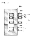
- Fig. 11 shows a construction view in a case where the winding T2 for load use and the tuning circuit winding T3 are split-wound. Even in this case, the T2S is connected with the T3S.
- the voltage difference between the T2E and the T3E is small, so that there is no possibility of the corona discharge and the arc discharge.
- the distance between the T2E and the T3E may be also made small, with the result that small-sized transformer made be made smaller. If the polarity is reverse, large voltage is caused between the T2E and the T3E to fail the transformer by the corona discharge and the arc discharge.
- the reverse voltage of the load 3 may be lowered by the provision of the resonance circuit means 1.
- the insulation of wirings, electrodes, terminals, etc. is not required to be strengthened, so that the realization is easier and the cost is lower.
- the generating voltage is dropped so that the stable power may be fed without the corona discharge and the arc discharge to be caused, the insulating withstand voltage between the windings of the transformer, the pulling of the wirings, and the insulating withstand voltage may be reduced.
- the distance between the windings of the transformer may be made smaller so that the transformer may be made smaller in size.
- the insulating yield strength is smaller and the size is smaller, the lower cost may be realized.
Landscapes
- Engineering & Computer Science (AREA)
- Power Engineering (AREA)
- Physics & Mathematics (AREA)
- Electromagnetism (AREA)
- Control Of High-Frequency Heating Circuits (AREA)
- Dc-Dc Converters (AREA)
- Cable Transmission Systems, Equalization Of Radio And Reduction Of Echo (AREA)
- General Induction Heating (AREA)
- Generation Of Surge Voltage And Current (AREA)
Claims (7)
- Appareil d'alimentation en énergie, comprenant une alimentation (9) telle qu'un réseau d'alimentation, une batterie d'accumulateurs ou analogue, un transducteur (14) d'énergie alimenté par l'alimentation (9) et comprenant un transformateur (2) ayant un primaire (T₁) et un secondaire (T₂, T₃) et au moins un commutateur à semi-conducteur (6) monté dans un circuit avec le primaire (T₁) et destiné à provoquer la création d'une tension de fonctionnement de sortie à haute fréquence aux bornes du secondaire (T₂) du transformateur afin qu'elle parvienne à une charge (3) qui a des caractéristiques de circulation unidirectionnelle de courant, caractérisé par un circuit résonnant (1) couplé à la sortie et accordé à une fréquence de résonance qui est un multiple impair de la fréquence de la tension de fonctionnement et donnant une tension de résonance, et dans lequel le circuit résonnant (1) est couplé au transducteur (14) d'énergie par un dispositif de couplage de manière que la forme d'onde de tension du circuit résonnant (1) se superpose à la forme d'onde de tension du transducteur d'énergie (14) et abaisse ainsi la tension inverse de la charge (3).
- Appareil d'alimentation en énergie selon la revendication 1, dans lequel la fréquence de résonance du circuit résonnant (1) est rendue pratiquement égale au troisième harmonique de la fréquence de fonctionnement du transducteur d'énergie (14).
- Appareil d'alimentation en énergie selon la revendication 1, dans lequel le circuit résonnant (1) est destiné à être connecté du côté du transformateur (2) tourné vers la charge.
- Appareil d'alimentation en énergie selon la revendication 1, dans lequel le circuit résonnant (1) est destiné à être connecté par le couplage magnétique du transformateur (2).
- Appareil d'alimentation en énergie selon la revendication 4, dans lequel le circuit (1) est destiné à être connecté par un enroulement (T₃) du transformateur (2).
- Appareil d'alimentation en énergie selon la revendication 5, dans lequel le circuit résonnant (1) est destiné à posséder une charge capacitive (C₃) connectée à l'enroulement (T₃) incorporé au transformateur (2).
- Appareil d'alimentation en énergie selon la revendication 5 ou 6, caractérisé en ce qu'une première borne de l'enroulement (T₃) du circuit résonnant (1) est connectée à une première borne du secondaire (T₂) qui est connectée à la charge (3) et les tensions respectives créées à l'autre borne de l'enroulement (T₃) du circuit résonnant (1) et à l'autre borne du secondaire (T₂) ont la même polarité.
Applications Claiming Priority (6)
| Application Number | Priority Date | Filing Date | Title |
|---|---|---|---|
| JP61298145A JPH0644513B2 (ja) | 1986-12-15 | 1986-12-15 | 高周波発生装置 |
| JP298144/86 | 1986-12-15 | ||
| JP298146/86 | 1986-12-15 | ||
| JP61298144A JPS63150882A (ja) | 1986-12-15 | 1986-12-15 | 電力供給装置 |
| JP298145/86 | 1986-12-15 | ||
| JP61298146A JPH0687427B2 (ja) | 1986-12-15 | 1986-12-15 | 高周波発生装置 |
Publications (3)
| Publication Number | Publication Date |
|---|---|
| EP0271850A2 EP0271850A2 (fr) | 1988-06-22 |
| EP0271850A3 EP0271850A3 (en) | 1989-11-23 |
| EP0271850B1 true EP0271850B1 (fr) | 1993-06-16 |
Family
ID=27338196
Family Applications (1)
| Application Number | Title | Priority Date | Filing Date |
|---|---|---|---|
| EP87118439A Expired - Lifetime EP0271850B1 (fr) | 1986-12-15 | 1987-12-12 | Appareil d'alimentation en puissance |
Country Status (6)
| Country | Link |
|---|---|
| US (1) | US4812960A (fr) |
| EP (1) | EP0271850B1 (fr) |
| KR (1) | KR900004348B1 (fr) |
| AU (1) | AU595083B2 (fr) |
| CA (1) | CA1290817C (fr) |
| DE (1) | DE3786238T2 (fr) |
Families Citing this family (10)
| Publication number | Priority date | Publication date | Assignee | Title |
|---|---|---|---|---|
| US4812960A (en) * | 1986-12-15 | 1989-03-14 | Matsushita Electric Industrial Co., Ltd. | Power feeding apparatus |
| EP0329386B1 (fr) * | 1988-02-18 | 1994-08-03 | MITSUI TOATSU CHEMICALS, Inc. | Résine de base de S-alkyl thiocarbamate, lentille plastique contenant cette résine et procédé pour la préparation de cette lentille |
| US4977301A (en) * | 1988-10-13 | 1990-12-11 | Matsushita Electric Industrial Co., Ltd. | High-frequency heating apparatus using frequency-converter-type power supply |
| US4858099A (en) * | 1988-12-08 | 1989-08-15 | France/Scott Fetzer Company | Resonant inverter |
| JPH0482191A (ja) * | 1990-07-25 | 1992-03-16 | Matsushita Electric Ind Co Ltd | 高周波加熱装置 |
| KR0115015Y1 (ko) * | 1991-09-19 | 1998-10-01 | 이헌조 | 스위칭소자 구동회로 |
| US5309343A (en) * | 1992-12-10 | 1994-05-03 | Schlenk Robert B | Driver circuit having paralleled transistors and current-variable resistive elements |
| US5790389A (en) * | 1996-05-31 | 1998-08-04 | Virginia Power Technologies, Inc. | Consolidated soft-switching AC/DC converters |
| ATE290035T1 (de) | 2000-12-15 | 2005-03-15 | Wellman Inc | Nachpolymerisierungs-spritzgiessen-verfahren bei der herstellung von kondensationspolymeren |
| TW569651B (en) * | 2002-07-05 | 2004-01-01 | Delta Electronics Inc | High-frequency heating device |
Family Cites Families (8)
| Publication number | Priority date | Publication date | Assignee | Title |
|---|---|---|---|---|
| US3319149A (en) * | 1963-08-08 | 1967-05-09 | Cole E K Ltd | Protective circuit arrangement for semiconductor switches in static inverters |
| JPS5028620B2 (fr) * | 1972-01-27 | 1975-09-17 | ||
| JPS5813652Y2 (ja) * | 1974-10-21 | 1983-03-16 | ソニー株式会社 | コウアツハツセイカイロ |
| US4616300A (en) * | 1982-12-17 | 1986-10-07 | Keltron Corporation | Method of and apparatus for efficient high voltage generation by resonant fly back |
| JPS61259488A (ja) * | 1985-05-14 | 1986-11-17 | 松下電器産業株式会社 | 高周波加熱装置 |
| EP0205642B1 (fr) * | 1985-06-24 | 1990-02-07 | Deutsche Thomson-Brandt GmbH | Convertisseur courant continu-courant continu |
| US4709316A (en) * | 1985-12-27 | 1987-11-24 | General Electric Company | Single-ended DC-to-DC converter with lossless switching |
| US4812960A (en) * | 1986-12-15 | 1989-03-14 | Matsushita Electric Industrial Co., Ltd. | Power feeding apparatus |
-
1987
- 1987-12-11 US US07/131,717 patent/US4812960A/en not_active Expired - Lifetime
- 1987-12-12 KR KR1019870014220A patent/KR900004348B1/ko not_active Expired
- 1987-12-12 DE DE8787118439T patent/DE3786238T2/de not_active Expired - Lifetime
- 1987-12-12 EP EP87118439A patent/EP0271850B1/fr not_active Expired - Lifetime
- 1987-12-15 AU AU82574/87A patent/AU595083B2/en not_active Ceased
- 1987-12-15 CA CA000554402A patent/CA1290817C/fr not_active Expired - Lifetime
Also Published As
| Publication number | Publication date |
|---|---|
| EP0271850A3 (en) | 1989-11-23 |
| US4812960A (en) | 1989-03-14 |
| EP0271850A2 (fr) | 1988-06-22 |
| KR880008501A (ko) | 1988-08-31 |
| AU595083B2 (en) | 1990-03-22 |
| AU8257487A (en) | 1988-06-16 |
| DE3786238T2 (de) | 1993-09-23 |
| DE3786238D1 (de) | 1993-07-22 |
| KR900004348B1 (ko) | 1990-06-22 |
| CA1290817C (fr) | 1991-10-15 |
Similar Documents
| Publication | Publication Date | Title |
|---|---|---|
| US6687137B1 (en) | Resonant switching power supply circuit with voltage doubler output | |
| US7889477B2 (en) | High voltage power supply for static neutralizers | |
| EP0923182B1 (fr) | Dispositif de transmission de puissance sans contact | |
| US6181079B1 (en) | High power electronic ballast with an integrated magnetic component | |
| US4560908A (en) | High-frequency oscillator-inverter ballast circuit for discharge lamps | |
| US4453109A (en) | Magnetic transformer switch and combination thereof with a discharge lamp | |
| EP0202579B1 (fr) | Appareil d'alimentation électrique pour une charge ayant des caractéristiques de blocage à l'arrière | |
| JPH0440837B2 (fr) | ||
| US4812960A (en) | Power feeding apparatus | |
| US5119285A (en) | Solid-state power transformer circuit | |
| KR20010050614A (ko) | 스위칭 전원 회로 | |
| US4701671A (en) | High-frequency oscillator-inverter ballast circuit for discharge lamps | |
| Sakamoto et al. | A novel circuit for non-contact charging through electro-magnetic coupling | |
| US6731521B2 (en) | Switching power supply circuit | |
| US4422015A (en) | Electric insect trap power supply | |
| US5962985A (en) | DC/AC converter with improved starter circuit | |
| US5032767A (en) | High frequency oscillator-inverter with improved regenerative power supply | |
| JP3152298B2 (ja) | 高圧電源回路 | |
| JP3735490B2 (ja) | 電子レンジ | |
| US6075327A (en) | Power supply apparatus for a discharge lamp, especially for a motor vehicle headlight | |
| JP3259337B2 (ja) | 電力変換装置 | |
| JPH0415599B2 (fr) | ||
| JPH0223108Y2 (fr) | ||
| EP0824300B1 (fr) | Convertisseur pour alimenter lampes à décharge comprenant des moyens d'amélioration du facteur de puissance | |
| JPH0538151A (ja) | 共振形電源回路 |
Legal Events
| Date | Code | Title | Description |
|---|---|---|---|
| PUAI | Public reference made under article 153(3) epc to a published international application that has entered the european phase |
Free format text: ORIGINAL CODE: 0009012 |
|
| 17P | Request for examination filed |
Effective date: 19871212 |
|
| AK | Designated contracting states |
Kind code of ref document: A2 Designated state(s): DE FR GB IT SE |
|
| PUAL | Search report despatched |
Free format text: ORIGINAL CODE: 0009013 |
|
| AK | Designated contracting states |
Kind code of ref document: A3 Designated state(s): DE FR GB IT SE |
|
| 17Q | First examination report despatched |
Effective date: 19911001 |
|
| GRAA | (expected) grant |
Free format text: ORIGINAL CODE: 0009210 |
|
| AK | Designated contracting states |
Kind code of ref document: B1 Designated state(s): DE FR GB IT SE |
|
| ITF | It: translation for a ep patent filed | ||
| REF | Corresponds to: |
Ref document number: 3786238 Country of ref document: DE Date of ref document: 19930722 |
|
| ET | Fr: translation filed | ||
| PLBE | No opposition filed within time limit |
Free format text: ORIGINAL CODE: 0009261 |
|
| STAA | Information on the status of an ep patent application or granted ep patent |
Free format text: STATUS: NO OPPOSITION FILED WITHIN TIME LIMIT |
|
| 26N | No opposition filed | ||
| EAL | Se: european patent in force in sweden |
Ref document number: 87118439.6 |
|
| ITPR | It: changes in ownership of a european patent |
Owner name: OFFERTA DI LICENZA AL PUBBLICO |
|
| REG | Reference to a national code |
Ref country code: GB Ref legal event code: 746 Effective date: 19950928 |
|
| REG | Reference to a national code |
Ref country code: FR Ref legal event code: D6 |
|
| REG | Reference to a national code |
Ref country code: GB Ref legal event code: IF02 |
|
| PGFP | Annual fee paid to national office [announced via postgrant information from national office to epo] |
Ref country code: SE Payment date: 20051206 Year of fee payment: 19 |
|
| PGFP | Annual fee paid to national office [announced via postgrant information from national office to epo] |
Ref country code: GB Payment date: 20061206 Year of fee payment: 20 |
|
| PGFP | Annual fee paid to national office [announced via postgrant information from national office to epo] |
Ref country code: DE Payment date: 20061207 Year of fee payment: 20 |
|
| PGFP | Annual fee paid to national office [announced via postgrant information from national office to epo] |
Ref country code: FR Payment date: 20061208 Year of fee payment: 20 |
|
| PG25 | Lapsed in a contracting state [announced via postgrant information from national office to epo] |
Ref country code: SE Free format text: LAPSE BECAUSE OF NON-PAYMENT OF DUE FEES Effective date: 20061213 |
|
| PGFP | Annual fee paid to national office [announced via postgrant information from national office to epo] |
Ref country code: IT Payment date: 20061231 Year of fee payment: 20 |
|
| EUG | Se: european patent has lapsed | ||
| REG | Reference to a national code |
Ref country code: GB Ref legal event code: PE20 |
|
| PG25 | Lapsed in a contracting state [announced via postgrant information from national office to epo] |
Ref country code: GB Free format text: LAPSE BECAUSE OF EXPIRATION OF PROTECTION Effective date: 20071211 |