EP0272833B1 - Bauelemente und Bauelemente-Herstellung mit Borsilikatglass - Google Patents
Bauelemente und Bauelemente-Herstellung mit Borsilikatglass Download PDFInfo
- Publication number
- EP0272833B1 EP0272833B1 EP87310778A EP87310778A EP0272833B1 EP 0272833 B1 EP0272833 B1 EP 0272833B1 EP 87310778 A EP87310778 A EP 87310778A EP 87310778 A EP87310778 A EP 87310778A EP 0272833 B1 EP0272833 B1 EP 0272833B1
- Authority
- EP
- European Patent Office
- Prior art keywords
- weight percent
- glass
- procedure
- semiconductor
- silica
- Prior art date
- Legal status (The legal status is an assumption and is not a legal conclusion. Google has not performed a legal analysis and makes no representation as to the accuracy of the status listed.)
- Expired - Lifetime
Links
Images


Classifications
-
- H—ELECTRICITY
- H10—SEMICONDUCTOR DEVICES; ELECTRIC SOLID-STATE DEVICES NOT OTHERWISE PROVIDED FOR
- H10P—GENERIC PROCESSES OR APPARATUS FOR THE MANUFACTURE OR TREATMENT OF DEVICES COVERED BY CLASS H10
- H10P14/00—Formation of materials, e.g. in the shape of layers or pillars
- H10P14/60—Formation of materials, e.g. in the shape of layers or pillars of insulating materials
- H10P14/69—Inorganic materials
- H10P14/692—Inorganic materials composed of oxides, glassy oxides or oxide-based glasses
- H10P14/6921—Inorganic materials composed of oxides, glassy oxides or oxide-based glasses containing silicon
- H10P14/6922—Inorganic materials composed of oxides, glassy oxides or oxide-based glasses containing silicon the material containing Si, O and at least one of H, N, C, F or other non-metal elements, e.g. SiOC, SiOC:H or SiONC
- H10P14/6923—Inorganic materials composed of oxides, glassy oxides or oxide-based glasses containing silicon the material containing Si, O and at least one of H, N, C, F or other non-metal elements, e.g. SiOC, SiOC:H or SiONC the material being boron or phosphorus doped silicon oxides, e.g. BPSG, BSG or PSG
-
- C—CHEMISTRY; METALLURGY
- C03—GLASS; MINERAL OR SLAG WOOL
- C03C—CHEMICAL COMPOSITION OF GLASSES, GLAZES OR VITREOUS ENAMELS; SURFACE TREATMENT OF GLASS; SURFACE TREATMENT OF FIBRES OR FILAMENTS MADE FROM GLASS, MINERALS OR SLAGS; JOINING GLASS TO GLASS OR OTHER MATERIALS
- C03C3/00—Glass compositions
- C03C3/04—Glass compositions containing silica
- C03C3/062—Glass compositions containing silica with less than 40% silica by weight
- C03C3/064—Glass compositions containing silica with less than 40% silica by weight containing boron
-
- C—CHEMISTRY; METALLURGY
- C03—GLASS; MINERAL OR SLAG WOOL
- C03C—CHEMICAL COMPOSITION OF GLASSES, GLAZES OR VITREOUS ENAMELS; SURFACE TREATMENT OF GLASS; SURFACE TREATMENT OF FIBRES OR FILAMENTS MADE FROM GLASS, MINERALS OR SLAGS; JOINING GLASS TO GLASS OR OTHER MATERIALS
- C03C3/00—Glass compositions
- C03C3/04—Glass compositions containing silica
- C03C3/076—Glass compositions containing silica with 40% to 90% silica, by weight
- C03C3/089—Glass compositions containing silica with 40% to 90% silica, by weight containing boron
- C03C3/091—Glass compositions containing silica with 40% to 90% silica, by weight containing boron containing aluminium
-
- H—ELECTRICITY
- H10—SEMICONDUCTOR DEVICES; ELECTRIC SOLID-STATE DEVICES NOT OTHERWISE PROVIDED FOR
- H10P—GENERIC PROCESSES OR APPARATUS FOR THE MANUFACTURE OR TREATMENT OF DEVICES COVERED BY CLASS H10
- H10P14/00—Formation of materials, e.g. in the shape of layers or pillars
- H10P14/60—Formation of materials, e.g. in the shape of layers or pillars of insulating materials
- H10P14/63—Formation of materials, e.g. in the shape of layers or pillars of insulating materials characterised by the formation processes
- H10P14/6326—Deposition processes
- H10P14/6328—Deposition from the gas or vapour phase
- H10P14/6329—Deposition from the gas or vapour phase using physical ablation of a target, e.g. physical vapour deposition or pulsed laser deposition
-
- H—ELECTRICITY
- H10—SEMICONDUCTOR DEVICES; ELECTRIC SOLID-STATE DEVICES NOT OTHERWISE PROVIDED FOR
- H10P—GENERIC PROCESSES OR APPARATUS FOR THE MANUFACTURE OR TREATMENT OF DEVICES COVERED BY CLASS H10
- H10P14/00—Formation of materials, e.g. in the shape of layers or pillars
- H10P14/60—Formation of materials, e.g. in the shape of layers or pillars of insulating materials
- H10P14/69—Inorganic materials
- H10P14/692—Inorganic materials composed of oxides, glassy oxides or oxide-based glasses
- H10P14/6921—Inorganic materials composed of oxides, glassy oxides or oxide-based glasses containing silicon
- H10P14/6928—Inorganic materials composed of oxides, glassy oxides or oxide-based glasses containing silicon the material containing silicon and at least one metal element, e.g. metal silicate based insulators or metal silicon oxynitrides
- H10P14/6929—Inorganic materials composed of oxides, glassy oxides or oxide-based glasses containing silicon the material containing silicon and at least one metal element, e.g. metal silicate based insulators or metal silicon oxynitrides the material containing aluminium, e.g. AlSiOx
-
- H—ELECTRICITY
- H10—SEMICONDUCTOR DEVICES; ELECTRIC SOLID-STATE DEVICES NOT OTHERWISE PROVIDED FOR
- H10P—GENERIC PROCESSES OR APPARATUS FOR THE MANUFACTURE OR TREATMENT OF DEVICES COVERED BY CLASS H10
- H10P14/00—Formation of materials, e.g. in the shape of layers or pillars
- H10P14/60—Formation of materials, e.g. in the shape of layers or pillars of insulating materials
- H10P14/69—Inorganic materials
- H10P14/692—Inorganic materials composed of oxides, glassy oxides or oxide-based glasses
- H10P14/6921—Inorganic materials composed of oxides, glassy oxides or oxide-based glasses containing silicon
- H10P14/6928—Inorganic materials composed of oxides, glassy oxides or oxide-based glasses containing silicon the material containing silicon and at least one metal element, e.g. metal silicate based insulators or metal silicon oxynitrides
- H10P14/6936—Inorganic materials composed of oxides, glassy oxides or oxide-based glasses containing silicon the material containing silicon and at least one metal element, e.g. metal silicate based insulators or metal silicon oxynitrides the material containing two or more metal elements
Definitions
- the invention is a process for making a semiconductor device in which a certain type of glass is used in the fabrication procedure and devices made by such processes.
- the fabrication of some semiconductor devices often requires capping layers for surface protection, pattern delineation, or as a barrier in annealing in various doping procedures.
- Such surface layers are useful during fabrication as well as on completed devices. Requirements for such films differ widely depending on the particular fabrication procedure, material, etc. Usually, adherence, stability (particularly toward moisture), and effectiveness as a diffusion barrier are of principal importance. Also, stability, adherence, etc., at high temperatures are desirable where high temperatures are used during fabrication of the device or on subsequent use of the device.
- the protective layer it might be advantageous for the protective layer to be at least partially transparent to radiation including radiation in the infrared, visible, ultraviolet, X-ray and gamma ray regions.
- stress conditions imposed by the glass layer may be critical to the use of various glass layers particularly where heat treatment of semiconducting compounds containing dopants is involved.
- Optical devices are becoming of increasing importance principally because of the development of optical communications systems and certain types of display systems. Because of these developments, various optical devices including semiconductor optical devices are becoming increasingly important so that economic and effective techniques for manufacturing such devices are in great demand. Coatings that are suitable for use on optical devices including semiconductor optical devices are highly desirable. Such coatings should be stable, unaffected by ordinary atmosphere substances such as moisture, chemicals, etc., adherent and be able to withstand temperatures used to fabricate the devices or in the use of the devices. In many devices, the coating should also be transparent at various parts of the radiation spectrum. Where the coating is used to encapsulate optical devices, it should be transparent to the part of the radiation spectrum where they operate. Exemplary optical devices are light emitting diodes, lasers and optical detectors.
- Coatings are often used as diffusion masks or capping layers in annealing procedures and in various other heat-treatment procedures, as well as for passivation.
- the layers should prevent diffusion of semiconductor material out through the glass layers or diffusion of doping material out through the glass layer.
- the thermal expansion properties of the glass layer also plays an important role in the heat-treatment procedure.
- optical is used in a broad sense and is not limited to visible radiation.
- optical radiation refers to any radiation and includes infrared radiation, ultraviolet radiation, X-ray and gamma ray radiation, etc.
- protective layers that are transparent to radiation.
- Typical semiconductor optical devices have been described in a variety of references including Light Emitting Diodes by A. A. Bergh and P. J. Dean, Clarenden Press, 1976, Injection Electroluminescent Devices by C. H. Gooch, John Wiley and Sons, New York, 1973, and Semiconductors and Semimetals, edited by R. K. Willardson and A. C. Beer, Academic Press, 1966, Vol. 2, Physics of III-V Compounds .
- Such devices include semiconductor lasers, opto-isolators, light emitting diodes, light detectors, solar cells, etc.
- the invention is a process for fabricating a semiconductor device in which the procedure includes deposition of a borosilicate glass layer by a particle beam deposition procedure where the borosilicate glass used in the particle beam deposition is a restructured or reconstituted borosilicate glass made by a phase separation procedure at a temperature less than 1500 degrees C.
- the preparation should be carried out a temperature less than 1400 or even 1300 degrees C.
- the glass preparation procedure involves mixing together SiO2, B2O3, Na2O and optionally other oxides (or precursors to oxides), heating to a temperature where the mixture melts, cooling and then exposing the resulting material to a heat treatment to separate the sodium borate phase from the silica-rich phase.
- the sodium borate phase is separated out from the silica-rich phase typically by leaching with an acid such as aqueous HCl. This leaves behind a porous silica-rich glass phase containing more than 90 weight percent SiO2. Another heat treatment often with the use of pressure may be used to remove pores and produce a fully dense material. Often, Al2O3 is included in the initial composition along with SiO2, B2O3 and Na2O to get better phase separation, reduce sodium content of the final product and improve the properties of the final, silica-rich product. This glass fabrication procedure is highly advantageous because temperatures in excess of 1500 degrees C are not required in the fabrication procedure and such glasses are available commercially (under the trade name VYCOR).
- This glass fabrication procedure yields a glass particularly useful for glass layers, in the fabrication of semiconductor devices, especially devices comprising III-V semiconductor compounds. These glass layers are particularly advantageous where heat treatments are used in the fabrication procedure. Such heat treatment procedures are often used as part of an ion implantation procedure to anneal damage caused by the implantation and activate the implanted material. Also included in the invention are devices made in accordance with the inventive process. Such devices have a number of unique features including unique passivating layers, unique doping profile, etc. Such devices exhibit unusually advantageous properties such as low dark current, low damage from ion implantation, etc. Particularly advantageous is the sharp, shallow doping profile which has a number of advantages for various devices including low pinch-off voltage for FETs, etc.
- the invention is based on the discovery that phase-separated, reconstituted glass when deposited by a particle beam deposition procedure (e.g. e-beam deposition) in the form of layers have unusally good properties as a barrier or encapsulating layers during processing or as a passivating layer on devices comprising silicon, III-V semiconductor compounds (e.g. GaAs, InP, etc.) and II-VI semiconductor compounds such as CdTe, HgSe and HgTe. Also of particular interest are III-V compounds which are lattice matched to either InP or GaAs such as InGaAs, InGaAsP, AlInAsP, etc.
- a boron-containing glass target is made by a specific procedure, and this target is used in the particle deposition procedure.
- Typical particle deposition procedures are e-beam deposition and sputtering.
- the specific procedure involves making a sodium borosilicate glass, effecting phase separation of the sodium borosilicate glass into a sodium-rich phase (e.g. sodium borate) and silica-rich phase and then removing the sodium-rich phase (e.g. by leaching or other chemical means) to leave a silica-rich phase.
- a sodium-rich phase e.g. sodium borate
- silica-rich phase e.g. sodium borate
- removing the sodium-rich phase e.g. by leaching or other chemical means
- Electron beam deposition is described in a number of references including Physical Vapor Deposition published by Airco Temescal (a division of Airco. Inc.), 2850 Seventh Street, Berkeley, California 94710. Sputtering is also described in a number of references including D.D. Davidse and L.I. Maissel in the Journal of Applied Physics, 37, pp. 574-79, 1966.
- the e-beam procedure is preferred because the surface of the semiconductor on which the glass is being deposited is less likely to be damaged and the deposition process involving e-beam is less likely to involve contamination of the semiconductor surface.
- the glass target has a high silica content, typically greater than 90 weight percent and preferably greater than 95 or even 96 or 97 weight percent.
- the glass target material also contains boron oxide generally in the concentration range from 1 to 15 weight percent preferably 1-6 weight percent.
- High silica content is desirable because of chemical stability, purity and the fact that undesirable, detrimental impurities are not introduced into the semiconductor during processing.
- the presence of boron is also highly desirable probably because it increases the thermal expansion of the glass layer so as to reduce strain of the glass layers in semiconductor surfaces. Also observed with boron present in the glass is much lower diffusion during annealing steps so as to yield more desirable doping profiles.
- alumina alumina
- Typical compositions are 96-97 weight percent silica, 0.1 to 0.9 weight percent Al2O3 and 2.0 to 4.0 weight percent B2O3.
- Glass target preparation involves a phase separation procedure which permits the use of much lower temperatures in the glass preparation procedure but still yields the three-dimensional structure necessary to make it useful for the fabrication of a good barrier glass layer.
- a mixture of Na2O, B2O3 and SiO2 is heated to a temperature between the melting temperature of the mixture and 1500 degrees C (typically 1100-1300 degrees C) for several minutes to several days. Times between 1 to 24 hours are preferred for convenience.
- Other oxides or precursors to oxides may be added, chiefly Al2O3, typically in the concentration range from 0.1 to 3.0 weight percent to promote better phase separation, improve the properties of the final product and lead to greater removal of sodium from the final product.
- Typical compositions of the initial mixture are 50-70 weight percent SiO2, 10-30 weight percent Na2O, 10-30 weight percent B2O3 and 0.2-2.5 weight percent other oxide, typically Al2O3.
- a sodium borosilicate glass is obtained.
- the sodium borosilicate glass may optionally be cast into a certain form (e.g., suitable for an e-beam target) at room temperature.
- the sodium borosilicate glass is then heat treated to effect phase separation. This heat treatment is typically between 600 and 900 degrees C for one hour to one day. This results in a material body with two coarsely separated phases; the sodium borate glass phase and the silica-rich glass phase.
- the sodium borate phase is then separated out from the silica-rich phase by conventional means usually by acid leaching each with an acid such as aqueous HCl.
- This material can often be used as is but more often is heat treated typically at about 1000-1200 degrees C for 1 hour to one day to remove pores and densify the material. This procedure is often called consolidating and sometimes involves the application of pressure.
- a commercial product such as VYCOR (particularly the product numbered 7913) is used as the glass target material in the particle deposition procedure. Indeed, much of the advantage of this procedure is the availability of commercial glasses of the type described above at reasonably low cost.
- a variety of procedures involving particle bombardment are used to deposit glass layers on semiconductor surfaces including e-beam deposition and sputtering.
- magnetron sputtering is used and the substrate is located remote from the plasma so as to avoid surface damage.
- Argon is generally used as the gas in the sputtering operation.
- the preferred deposition procedure is e-beam deposition. Advantages of this procedure are low contamination level, reasonable deposition rates where the structure of the glass is largely preserved and easy provision to control the temperature of the surface on which the deposition is being made.
- the semiconductor surface, upon which the glass is deposited generally is not damaged or otherwise affected by the e-beam procedure.
- the e-beam deposition procedure is conventional. Generally, the surfaces of interest are exposed to an aqueous HF solution for a short time (e.g., about 30 seconds), rinsed in deionized water and dried before deposition. The temperature of the surface is between room temperature and 350 degrees C with 250-300 preferred. Typical e-beam evaporator pressures are less than or equal to (5x10 ⁇ 6 torr.) 666 ⁇ 7 Pascals.
- the thickness of the glass films may vary over large limits including from about (50 to 5000 ⁇ ngstroms) 5x10 ⁇ 9m to 5x10 ⁇ 7m, but for many applications (annealing ion implanted samples) from (300-1500 ⁇ ngstroms) (3x10 ⁇ 8m to 15x10 ⁇ 8m) yield excellent results. For less than (300 ⁇ ngstroms) 3x10 ⁇ 8m, the anneal procedure sometimes yields undesirable results. Thicker films yields perfectly good results but are often wasteful of time and material.
- a particularly good application of the reconstituted glass is in the activation step in an ion-implant process.
- dopant ions are ion implanted into semiconductor compounds.
- the sample is annealed or heat treated to remove damage caused by the ion implantation and to activate the dopant ions.
- the glass is used as the capping layer in the heat treatment. Ion implantation may be carried out before deposition of the glass layer or through the glass layer after deposition of the glass layer. These glass layers may also be used as encapsulants or protective layers permanently attached to the surface of the device.
- ions can be used in the ion implantation process. These ions include both n-type (donor) ions and p-type (acceptor) ions.
- donor ions for III-V compounds are silicon, germanium, tin, sulfur, selenium and tellurium.
- acceptor ions for III-V compounds are zinc, cadmium, mercury, beryllium, magnesium and managanese.
- typical n-type dopants are phorphorus and arsenic; a typical p-type dopant is boron.
- FIG. 1 shows a planar InP/InGaAs-APD (avalanche photodetector) structure made in accordance with the invention.
- the photodetector 10 is made up of a substrate 11 (doping level approximately 5x10¹⁷ sulfur atoms/cm3) with a number of epitaxial layers generally put down by vapor phase epitaxy.
- n-InP layer 12 Immediately above the substrate 11 is an n-InP layer 12 (doping level approximately 1-2x10¹⁶ sulfur atoms/cm3) followed by the absorption layer 13 (n-type InGaAs with composition lattice matched to InP and undoped but carrier concentration between 1-10x10+14 per cm3) and then a thin layer 14 of n-InGaAsP with lower bandgap than InGaAs to speed up the response of the device.
- n-InP layer 12 doping level approximately 1-2x10¹⁶ sulfur atoms/cm3
- the absorption layer 13 n-type InGaAs with composition lattice matched to InP and undoped but carrier concentration between 1-10x10+14 per cm3
- a thin layer 14 of n-InGaAsP with lower bandgap than InGaAs to speed up the response of the device.
- n+-InP layer 15 often called the multiplication layer made up of sulfur doped indium phosphide in the concentration range of 1-2x10¹⁶ atoms/cm3 and then a layer 16 of n-InP (undoped indium phosphide with carrier concentration about 1-10x1014 carriers/cm3).
- Guard rings 17 are put down in this layer using ion implantation and the restructured reconstituted glass described above. Glass layers deposited by e-beam deposition are used in this procedure to prevent out diffusion during annealing in the ion impregnation-annealing procedure. It also maintains the integrity of the surface during annealing and minimizes diffusion of the dopant ions during annealing.
- a glass layer is deposited over the entire n-InP layer, beryllium implanted through the glass layer and into the n-InP layer 16 to form the guard rings 17 and the layer exposed to rapid thermal anneal (typically 800-850 degrees C for 5 to 15 seconds) or conventional anneal (typically 700-750 degrees C for 5 to 15 minutes).
- rapid thermal anneal typically 800-850 degrees C for 5 to 15 seconds
- conventional anneal typically 700-750 degrees C for 5 to 15 minutes.
- An alternate procedure includes deposition of a glass layer in accordance with the invention on the back face of the substrate prior to rapid thermal anneal and then removal of this glass layer prior to further processing on this back face.
- the diode part 18 of the n-InP layer (the p+-InP in layer 16) may be made by diffusion of cadmium or zinc through a hole opened in the glass layer or ion impregnation through the glass layer followed by rapid thermal anneal.
- the electrode 19 is generally gold over chromium.
- the dielectric layer may be silicon nitride or preferably restructured glass originally put down for the ion implantation procedure. Where both diode region 18 and guard ring region 17 are done by ion implantation, a single annealing step (e.g., rapid thermal anneal) may be used for both regions. Electrodes 21 are also put on the bottom of the device as well as an antireflection coating 22 (e.g., silicon nitride) where the radiation enters.
- an antireflection coating 22 e.g., silicon nitride
- the glass layer thickness is generally about (1000 to 2000 ⁇ ngstroms) 1x10 ⁇ 7m to 2x10 ⁇ 7m and the surface temperature of the semiconductor surface on which the glass is deposited is from 200 to 300 degrees C.
- Avalanche photodetectors made in accordance with the invention have unusually good characteristics, especially as to low dark current.
- Low dark current is advantageous because dark current is a source of noise.
- FIG. 2 shows a plot of dark current vs. reverse bias voltage for photodetectors made by using restructured glass layers and ones made by use of phosphosilicate glass.
- Such an improvement has a significant effect on device performance, noise characteristics and response time.
- improved device performance has considerable economic repercussions in optical communication system design including greater spacing between repeaters, lower error rates, higher data transmission rates, etc.
- GaAs substrates were liquid encapsulated Czochralski (LEC) grown, undoped (100) GaAs wafers of 5 cm diameter. The procedure was carried out on polished wafers of GaAs. A chemical-mechanical polishing procedure using bromine-methanol was used to remove about 50 ⁇ m of the surface of the wafers. The wafers were then degreased in boiling trichlorethylene, acetone and methanol and rinsed in deionized water. Finally, they were etched for 3 minutes in a freshly prepared solution of 5H2SO4:1H2O at 70 degrees C, followed by a thorough rinse in deionized water and dried with filtered dry nitrogen.
- LOC liquid encapsulated Czochralski
- the glass target for the e-beam deposition is obtained by the phase separation procedure described above. Often, the glass target is obtained as a commercial product such as VYCOR (particularly the product numbered 7913) is used as the glass target material in the particle deposition procedure.
- VYCOR particularly the product numbered 7913
- a rapid thermal anneal procedure was used as a post implant anneal procedure. This procedure is carried out in the e-beam evaporation apparatus using tungsten lamps as heat sources. Typical rapid thermal anneal procedures involve temperatures of 900 to 1000 degrees C for 3-10 seconds.
- the films were easily removed in either a 1HF:1H20 solution for about 2 minutes or in a CF4 plasma etcher for about 10 minutes. No peeling-off or blistering of films was observed after annealing up to temperatures in excess of 950 degrees C. Films stored for more than six months did not deteriorate with regard to their ability as effective encapsulants.
- Carrier concentration versus depth profiles were determined by the C-V profiling method at the frequency of 10 kHz.
- the C-V measurements were carried out using a mercury probe to form Schottky barrier contacts.
- the average mobility was obtained by Hall-effect measurements using the Van der Pauw technique.
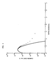
- FIG. 3 and FIG. 4 show doping profiles of two GaAs samples implanted and annealed as described above.
- the rapid thermal anneal following implantation was at about 955 degrees C for 6 seconds and the glass was deposited at room temperature.
- the rapid thermal anneal was carried out under about the same conditions (990 degrees C for 5 seconds) and the glass layer deposited at 230 degrees C.
Landscapes
- Chemical & Material Sciences (AREA)
- Materials Engineering (AREA)
- Engineering & Computer Science (AREA)
- Chemical Kinetics & Catalysis (AREA)
- General Chemical & Material Sciences (AREA)
- Geochemistry & Mineralogy (AREA)
- Life Sciences & Earth Sciences (AREA)
- Organic Chemistry (AREA)
- Formation Of Insulating Films (AREA)
- Recrystallisation Techniques (AREA)
- Glass Compositions (AREA)
- Light Receiving Elements (AREA)
- Led Devices (AREA)
Claims (10)
- Verfahren zur Herstellung einer Halbleitervorrichtung mit dem Schritt des Aufbringens eines Glastargetmaterials auf mindestens einen Teil der Halbleiteroberfläche durch ein Partikelstrahlabscheidungsverfahren zur Bildung eines Glasmaterialbereichs, der die Halbleiteroberfläche berührt, wobei der Glasmaterialbereich mindestens 1 Gew.% BeO₃ und mindestens 90 Gew.% SiO₂ enthält,
dadurch gekennzeichnet,
daß das Glasmaterial durch folgende Verfahrensschritte hergestellt worden ist:a. Herstellung eines Natriumborsilicatglases mit einem Gehalt an Natriumborsilicat;b. Durchführung der Phasentrennung des Natriumborsilicatglases in eine natriumreiche und eine siliciumreiche Phase durch Wärmebehandlung im Temperaturbereich von 600 bis 900°C;c. Trennen der natriumreichen Phase von der siliciumreichen Phase durch Auslaugen mit einer Säure;d. gegebenenfalls Konsolidieren der siliciumreichen Phase durch Wärmebehandlung während einer Stunde bis zu einem Tag. - Verfahren nach Anspruch 1,
dadurch gekennzeichnet,
daß das Partikelstrahlaufbringungsverfahren ein Elektronenstrahlabscheidungsverfahren ist. - Verfahren nach Anspruch 1,
dadurch gekennzeichnet,
daß die Halbleiteroberfläche eine Siliciumoberfläche ist. - Verfahren nach Anspruch 1,
dadurch gekennzeichnet,
daß der Halbleiter eine III-V-Halbleiterverbindung umfaßt. - Verfahren nach Anspruch 4,
dadurch gekennzeichnet,
daß die III-V-Halbleiterverbindung aus der Gruppe bestehend aus InP und GaAs ausgewählt wird und das Kristallgitter der Verbindungen zu InP und GaAs paßt. - Verfahren nach Anspruch 1,
dadurch gekennzeichnet,
daß der Glasmaterialbereich mindestens 95 Gew.% Silicat und 1 bis 5 Gew.% Boroxid enthält. - Verfahren nach Anspruch 6,
dadurch gekennzeichnet,
daß der Glasmaterialbereich aus 96 bis 97 Gew.% Silicat, 0,1 bis 0,9 Gew.% Al₂O₃ und 2,0 bis 4,0 Gew.% B₂O₃ besteht. - Verfahren nach Anspruch 1,
dadurch gekennzeichnet,
daß das Natriumborsilicatglas mit dem Gehalt an Natriumborsilicat durch Erhitzen einer Mischung aus Na₂O, B₂O₃ und SiO₂ auf eine Temperatur zwischen der Schmelztemperatur der Mischung und 500°C hergestellt wird. - Verfahren nach Anspruch 8,
dadurch gekennzeichnet,
daß die Mischung zusätzlich zu Na₂O, B₂O₃ und SiO2 zwischen 0,1 und 0,3 Gew.% Al₂O₃ enthält. - Verfahren nach Anspruch 8,
dadurch gekennzeichnet,
daß die ursprüngliche Ausgangsmischung aus 50 bis 70 Gew.% SiO₂, 10 bis 30 Gew.% Na₂O, 10 bis 30 Gew.% B₂O₃ und 0,2 bis 2,5 Gew.% Al₂O₃ besteht.
Applications Claiming Priority (2)
| Application Number | Priority Date | Filing Date | Title |
|---|---|---|---|
| US06/945,016 US4819039A (en) | 1986-12-22 | 1986-12-22 | Devices and device fabrication with borosilicate glass |
| US945016 | 1986-12-22 |
Publications (2)
| Publication Number | Publication Date |
|---|---|
| EP0272833A1 EP0272833A1 (de) | 1988-06-29 |
| EP0272833B1 true EP0272833B1 (de) | 1992-07-22 |
Family
ID=25482478
Family Applications (1)
| Application Number | Title | Priority Date | Filing Date |
|---|---|---|---|
| EP87310778A Expired - Lifetime EP0272833B1 (de) | 1986-12-22 | 1987-12-08 | Bauelemente und Bauelemente-Herstellung mit Borsilikatglass |
Country Status (5)
| Country | Link |
|---|---|
| US (1) | US4819039A (de) |
| EP (1) | EP0272833B1 (de) |
| JP (1) | JPH0732265B2 (de) |
| CA (1) | CA1321123C (de) |
| DE (1) | DE3780598T2 (de) |
Families Citing this family (17)
| Publication number | Priority date | Publication date | Assignee | Title |
|---|---|---|---|---|
| US4955031A (en) * | 1988-07-12 | 1990-09-04 | University Of Connecticut | Metal insulator semiconductor heterostructure lasers |
| GB8817886D0 (en) * | 1988-07-27 | 1988-09-01 | British Telecomm | Avalanche photodiode structure |
| US5221367A (en) * | 1988-08-03 | 1993-06-22 | International Business Machines, Corp. | Strained defect-free epitaxial mismatched heterostructures and method of fabrication |
| US5047369A (en) * | 1989-05-01 | 1991-09-10 | At&T Bell Laboratories | Fabrication of semiconductor devices using phosphosilicate glasses |
| JPH04111477A (ja) * | 1990-08-31 | 1992-04-13 | Sumitomo Electric Ind Ltd | 受光素子 |
| US5412229A (en) * | 1990-08-31 | 1995-05-02 | Sumitomo Electric Industries, Ltd. | Semiconductor light detecting device making use of a photodiode chip |
| US6105006A (en) * | 1997-12-22 | 2000-08-15 | Motorola Inc | Transaction authentication for 1-way wireless financial messaging units |
| US6208680B1 (en) | 1997-12-23 | 2001-03-27 | Lucent Technologies Inc. | Optical devices having ZNS/CA-MG-fluoride multi-layered mirrors |
| US6044100A (en) * | 1997-12-23 | 2000-03-28 | Lucent Technologies Inc. | Lateral injection VCSEL |
| US6169756B1 (en) | 1997-12-23 | 2001-01-02 | Lucent Technologies Inc. | Vertical cavity surface-emitting laser with optical guide and current aperture |
| CA2307745A1 (en) * | 1999-07-15 | 2001-01-15 | Sumitomo Electric Industries, Ltd. | Photodiode |
| CN1656612A (zh) * | 2002-05-23 | 2005-08-17 | 肖特股份公司 | 用于高频的玻璃材料 |
| US20050181177A1 (en) * | 2004-02-18 | 2005-08-18 | Jamie Knapp | Isotropic glass-like conformal coatings and methods for applying same to non-planar substrate surfaces at microscopic levels |
| EP2118029B1 (de) * | 2007-02-28 | 2017-07-12 | Corning Incorporated | Verfahren zur herstellung extrudierter glasstrukturen |
| JP4948458B2 (ja) * | 2008-03-19 | 2012-06-06 | 三洋電機株式会社 | 太陽電池の製造方法及び太陽電池 |
| US9985158B2 (en) | 2012-06-13 | 2018-05-29 | Massachusetts Institute Of Technology | Visibly transparent, luminescent solar concentrator |
| WO2016100450A1 (en) | 2014-12-17 | 2016-06-23 | Novartis Ag | Reusable lens molds and methods of use thereof |
Family Cites Families (8)
| Publication number | Priority date | Publication date | Assignee | Title |
|---|---|---|---|---|
| US2106744A (en) * | 1934-03-19 | 1938-02-01 | Corning Glass Works | Treated borosilicate glass |
| US2221709A (en) * | 1938-01-29 | 1940-11-12 | Corning Glass Works | Borosilicate glass |
| NL242742A (de) * | 1958-09-04 | |||
| US4228446A (en) * | 1979-05-10 | 1980-10-14 | Rca Corporation | Reduced blooming device having enhanced quantum efficiency |
| US4374391A (en) * | 1980-09-24 | 1983-02-15 | Bell Telephone Laboratories, Incorporated | Device fabrication procedure |
| US4492717A (en) * | 1981-07-27 | 1985-01-08 | International Business Machines Corporation | Method for forming a planarized integrated circuit |
| JPS59150492A (ja) * | 1983-02-04 | 1984-08-28 | 株式会社東芝 | 厚膜多層基板の製造方法 |
| FR2558152B1 (fr) * | 1984-01-13 | 1992-03-27 | Corning Glass Works | Verres a usage ophtalmique de faible densite, absorbant les radiations ultraviolettes et ayant une haute transmission dans le visible et lentilles correctrices constituees de ces verres |
-
1986
- 1986-12-22 US US06/945,016 patent/US4819039A/en not_active Expired - Lifetime
-
1987
- 1987-11-30 CA CA000553140A patent/CA1321123C/en not_active Expired - Fee Related
- 1987-12-08 DE DE8787310778T patent/DE3780598T2/de not_active Expired - Lifetime
- 1987-12-08 EP EP87310778A patent/EP0272833B1/de not_active Expired - Lifetime
- 1987-12-22 JP JP32305287A patent/JPH0732265B2/ja not_active Expired - Lifetime
Also Published As
| Publication number | Publication date |
|---|---|
| DE3780598T2 (de) | 1992-12-10 |
| DE3780598D1 (de) | 1992-08-27 |
| EP0272833A1 (de) | 1988-06-29 |
| CA1321123C (en) | 1993-08-10 |
| JPS63175431A (ja) | 1988-07-19 |
| US4819039A (en) | 1989-04-04 |
| JPH0732265B2 (ja) | 1995-04-10 |
Similar Documents
| Publication | Publication Date | Title |
|---|---|---|
| US4819039A (en) | Devices and device fabrication with borosilicate glass | |
| US4374391A (en) | Device fabrication procedure | |
| US5173443A (en) | Method of manufacture of optically transparent electrically conductive semiconductor windows | |
| US4615766A (en) | Silicon cap for annealing gallium arsenide | |
| Kasahara et al. | Capless anneal of ion‐implanted GaAs in controlled arsenic vapor | |
| CA1250055A (en) | Coating of iii-v and ii-vi compound semiconductors | |
| US4731293A (en) | Fabrication of devices using phosphorus glasses | |
| EP0128724B2 (de) | Herstellung von Photodioden | |
| JPH10289906A5 (de) | ||
| Oberstar et al. | Thin film encapsulants for annealing GaAs and InP | |
| Hunsperger et al. | Electrical properties of zinc and cadmium ion implanted layers in gallium arsenide | |
| US4267014A (en) | Semiconductor encapsulant for annealing ion-implanted GaAs | |
| US4089714A (en) | Doping mercury cadmium telluride with aluminum or silicon | |
| US4502898A (en) | Diffusion procedure for semiconductor compound | |
| JP2878746B2 (ja) | 光透過型電気伝導性半導体ウィンドー | |
| US4087293A (en) | Silicon as donor dopant in Hg1-x Cdx Te | |
| Tsuo et al. | Hydrogen passivation of silicon sheet solar cells | |
| US4105479A (en) | Preparation of halogen doped mercury cadmium telluride | |
| Kim et al. | Photoluminescence study of heat‐treated InP | |
| WO2013168135A1 (en) | A process for the manufacture of thin film solar cells | |
| US4089713A (en) | Diffusion of donors into (Hg Cd) Te through use of Ga-Al alloy | |
| JPS6154619A (ja) | 砒化ガリウムp型伝導層の形成方法 | |
| Feldman et al. | Antimony doping in vacuum deposited thin film silicon photovoltaic cells | |
| RU2023326C1 (ru) | СПОСОБ СОЗДАНИЯ НА ОБРАЗЦАХ CdxHg1-xTe P-ТИПА СТРУКТУР С ГЛУБОКОКОМПЕНСИРОВАННЫМ СЛОЕМ | |
| Skromme et al. | Rapid Thermal Annealing and Ion Implantation of Heteroepitaxial ZnSe/GaAs |
Legal Events
| Date | Code | Title | Description |
|---|---|---|---|
| PUAI | Public reference made under article 153(3) epc to a published international application that has entered the european phase |
Free format text: ORIGINAL CODE: 0009012 |
|
| AK | Designated contracting states |
Kind code of ref document: A1 Designated state(s): DE FR GB IT NL |
|
| 17P | Request for examination filed |
Effective date: 19881214 |
|
| 17Q | First examination report despatched |
Effective date: 19910521 |
|
| GRAA | (expected) grant |
Free format text: ORIGINAL CODE: 0009210 |
|
| AK | Designated contracting states |
Kind code of ref document: B1 Designated state(s): DE FR GB IT NL |
|
| REF | Corresponds to: |
Ref document number: 3780598 Country of ref document: DE Date of ref document: 19920827 |
|
| ET | Fr: translation filed | ||
| ITF | It: translation for a ep patent filed | ||
| PLBE | No opposition filed within time limit |
Free format text: ORIGINAL CODE: 0009261 |
|
| STAA | Information on the status of an ep patent application or granted ep patent |
Free format text: STATUS: NO OPPOSITION FILED WITHIN TIME LIMIT |
|
| 26N | No opposition filed | ||
| PGFP | Annual fee paid to national office [announced via postgrant information from national office to epo] |
Ref country code: FR Payment date: 20001128 Year of fee payment: 14 |
|
| PGFP | Annual fee paid to national office [announced via postgrant information from national office to epo] |
Ref country code: NL Payment date: 20001130 Year of fee payment: 14 |
|
| PGFP | Annual fee paid to national office [announced via postgrant information from national office to epo] |
Ref country code: GB Payment date: 20001201 Year of fee payment: 14 |
|
| PGFP | Annual fee paid to national office [announced via postgrant information from national office to epo] |
Ref country code: DE Payment date: 20001229 Year of fee payment: 14 |
|
| PG25 | Lapsed in a contracting state [announced via postgrant information from national office to epo] |
Ref country code: GB Free format text: LAPSE BECAUSE OF NON-PAYMENT OF DUE FEES Effective date: 20011208 |
|
| REG | Reference to a national code |
Ref country code: GB Ref legal event code: IF02 |
|
| PG25 | Lapsed in a contracting state [announced via postgrant information from national office to epo] |
Ref country code: NL Free format text: LAPSE BECAUSE OF NON-PAYMENT OF DUE FEES Effective date: 20020701 |
|
| PG25 | Lapsed in a contracting state [announced via postgrant information from national office to epo] |
Ref country code: DE Free format text: LAPSE BECAUSE OF NON-PAYMENT OF DUE FEES Effective date: 20020702 |
|
| GBPC | Gb: european patent ceased through non-payment of renewal fee |
Effective date: 20011208 |
|
| PG25 | Lapsed in a contracting state [announced via postgrant information from national office to epo] |
Ref country code: FR Free format text: LAPSE BECAUSE OF NON-PAYMENT OF DUE FEES Effective date: 20020830 |
|
| NLV4 | Nl: lapsed or anulled due to non-payment of the annual fee |
Effective date: 20020701 |
|
| REG | Reference to a national code |
Ref country code: FR Ref legal event code: ST |
|
| PG25 | Lapsed in a contracting state [announced via postgrant information from national office to epo] |
Ref country code: IT Free format text: LAPSE BECAUSE OF NON-PAYMENT OF DUE FEES;WARNING: LAPSES OF ITALIAN PATENTS WITH EFFECTIVE DATE BEFORE 2007 MAY HAVE OCCURRED AT ANY TIME BEFORE 2007. THE CORRECT EFFECTIVE DATE MAY BE DIFFERENT FROM THE ONE RECORDED. Effective date: 20051208 |