EP0128724B2 - Herstellung von Photodioden - Google Patents
Herstellung von Photodioden Download PDFInfo
- Publication number
- EP0128724B2 EP0128724B2 EP84303761A EP84303761A EP0128724B2 EP 0128724 B2 EP0128724 B2 EP 0128724B2 EP 84303761 A EP84303761 A EP 84303761A EP 84303761 A EP84303761 A EP 84303761A EP 0128724 B2 EP0128724 B2 EP 0128724B2
- Authority
- EP
- European Patent Office
- Prior art keywords
- layer
- degrees
- temperature
- capping
- active
- Prior art date
- Legal status (The legal status is an assumption and is not a legal conclusion. Google has not performed a legal analysis and makes no representation as to the accuracy of the status listed.)
- Expired - Lifetime
Links
Images
Classifications
-
- H—ELECTRICITY
- H10—SEMICONDUCTOR DEVICES; ELECTRIC SOLID-STATE DEVICES NOT OTHERWISE PROVIDED FOR
- H10P—GENERIC PROCESSES OR APPARATUS FOR THE MANUFACTURE OR TREATMENT OF DEVICES COVERED BY CLASS H10
- H10P95/00—Generic processes or apparatus for manufacture or treatments not covered by the other groups of this subclass
-
- H—ELECTRICITY
- H10—SEMICONDUCTOR DEVICES; ELECTRIC SOLID-STATE DEVICES NOT OTHERWISE PROVIDED FOR
- H10P—GENERIC PROCESSES OR APPARATUS FOR THE MANUFACTURE OR TREATMENT OF DEVICES COVERED BY CLASS H10
- H10P14/00—Formation of materials, e.g. in the shape of layers or pillars
- H10P14/60—Formation of materials, e.g. in the shape of layers or pillars of insulating materials
- H10P14/69—Inorganic materials
- H10P14/694—Inorganic materials composed of nitrides
- H10P14/6943—Inorganic materials composed of nitrides containing silicon
- H10P14/69433—Inorganic materials composed of nitrides containing silicon the material being a silicon nitride not containing oxygen, e.g. SixNy or SixByNz
-
- H—ELECTRICITY
- H10—SEMICONDUCTOR DEVICES; ELECTRIC SOLID-STATE DEVICES NOT OTHERWISE PROVIDED FOR
- H10F—INORGANIC SEMICONDUCTOR DEVICES SENSITIVE TO INFRARED RADIATION, LIGHT, ELECTROMAGNETIC RADIATION OF SHORTER WAVELENGTH OR CORPUSCULAR RADIATION
- H10F71/00—Manufacture or treatment of devices covered by this subclass
- H10F71/127—The active layers comprising only Group III-V materials, e.g. GaAs or InP
- H10F71/1272—The active layers comprising only Group III-V materials, e.g. GaAs or InP comprising at least three elements, e.g. GaAlAs or InGaAsP
-
- H—ELECTRICITY
- H10—SEMICONDUCTOR DEVICES; ELECTRIC SOLID-STATE DEVICES NOT OTHERWISE PROVIDED FOR
- H10F—INORGANIC SEMICONDUCTOR DEVICES SENSITIVE TO INFRARED RADIATION, LIGHT, ELECTROMAGNETIC RADIATION OF SHORTER WAVELENGTH OR CORPUSCULAR RADIATION
- H10F71/00—Manufacture or treatment of devices covered by this subclass
- H10F71/129—Passivating
-
- H—ELECTRICITY
- H10—SEMICONDUCTOR DEVICES; ELECTRIC SOLID-STATE DEVICES NOT OTHERWISE PROVIDED FOR
- H10F—INORGANIC SEMICONDUCTOR DEVICES SENSITIVE TO INFRARED RADIATION, LIGHT, ELECTROMAGNETIC RADIATION OF SHORTER WAVELENGTH OR CORPUSCULAR RADIATION
- H10F77/00—Constructional details of devices covered by this subclass
-
- H—ELECTRICITY
- H10—SEMICONDUCTOR DEVICES; ELECTRIC SOLID-STATE DEVICES NOT OTHERWISE PROVIDED FOR
- H10F—INORGANIC SEMICONDUCTOR DEVICES SENSITIVE TO INFRARED RADIATION, LIGHT, ELECTROMAGNETIC RADIATION OF SHORTER WAVELENGTH OR CORPUSCULAR RADIATION
- H10F77/00—Constructional details of devices covered by this subclass
- H10F77/30—Coatings
- H10F77/306—Coatings for devices having potential barriers
-
- Y—GENERAL TAGGING OF NEW TECHNOLOGICAL DEVELOPMENTS; GENERAL TAGGING OF CROSS-SECTIONAL TECHNOLOGIES SPANNING OVER SEVERAL SECTIONS OF THE IPC; TECHNICAL SUBJECTS COVERED BY FORMER USPC CROSS-REFERENCE ART COLLECTIONS [XRACs] AND DIGESTS
- Y02—TECHNOLOGIES OR APPLICATIONS FOR MITIGATION OR ADAPTATION AGAINST CLIMATE CHANGE
- Y02E—REDUCTION OF GREENHOUSE GAS [GHG] EMISSIONS, RELATED TO ENERGY GENERATION, TRANSMISSION OR DISTRIBUTION
- Y02E10/00—Energy generation through renewable energy sources
- Y02E10/50—Photovoltaic [PV] energy
- Y02E10/544—Solar cells from Group III-V materials
-
- Y—GENERAL TAGGING OF NEW TECHNOLOGICAL DEVELOPMENTS; GENERAL TAGGING OF CROSS-SECTIONAL TECHNOLOGIES SPANNING OVER SEVERAL SECTIONS OF THE IPC; TECHNICAL SUBJECTS COVERED BY FORMER USPC CROSS-REFERENCE ART COLLECTIONS [XRACs] AND DIGESTS
- Y10—TECHNICAL SUBJECTS COVERED BY FORMER USPC
- Y10S—TECHNICAL SUBJECTS COVERED BY FORMER USPC CROSS-REFERENCE ART COLLECTIONS [XRACs] AND DIGESTS
- Y10S438/00—Semiconductor device manufacturing: process
- Y10S438/902—Capping layer
Definitions
- the invention relates to procedures for making photodetectors using compound semiconductors formed on substrates containing phosphorus, for example photodetectors formed in InGaAs or InGaAsP films grown on substrates containing InP.
- optical communication systems have led to considerable activity in the optical device field.
- Various devices are of importance in optical communication systems, including sources (light-emitting diodes, lasers), transmission media (optical fibres) and detectors.
- sources light-emitting diodes, lasers
- transmission media optical fibres
- detectors The quality and characteristics of these devices (as well as other devices in the system) contribute significantly to the quality and efficiency of the optical communication system.
- a particularly important part of the optical communication system is the photodetector. It contributes significantly to the sensitivity of the receiver in an optical communication system and often determines repeater spacing in an optical communication system. Particularly important is the noise generated at the photodetector and the bandwidth of the photodetector.
- photodetectors are made with compound semiconductors containing phosphorus.
- compound semiconductors containing phosphorus For example, for many photodetector devices operating at about 1.3 ⁇ m (i.e., the 1.25-1.35 ⁇ m region), InP is conveniently used as a substrate material and an epitaxially grown material such as InGaAs is used as the active material. In such devices, low noise is particularly important especially where these photodetectors are used in optical communication systems.
- An especially important source of noise in photodetectors is dark current. It is highly desirable to minimize dark current in photodetectors because it adversely affects noise performance. Improved noise performance makes possible improved performance in a variety of optical systems including optical communication systems.
- a process as set out in the preamble of claim 1 is disclosed by Suza and others in ⁇ Plasma enhanced CVD Si3N4 film applied to InP avalanche photodiodes', Japanese Journal of Applied Physics, Vol 19, No 11, November 1980, pages L675-L678.
- the Si3N4 capping layer is deposited by a low-temperature process, the substrates being kept at 250-300°C throughout.
- Various protective layers are useful to produce effective passivation without raising the sample temperature above about 250 to 300 degrees C.
- Particularly useful as a protective layer is silicon nitride (SiN x ) put down by plasma chemical vapour deposition.
- a particularly useful procedure is to deposit a limited thickness of dielectric (generally 20 to 50 nanometres and preferably 30 nanometres) at a temperature less than 250 degrees C and then the remaining thickness (generally up to about 5 micrometres) at less than 400 degrees C.
- Photodetectors sensitive in the 1.0-1.6 ⁇ m region can be made with InP substrates and active regions of InGaAs (typical composition about In 0.53 Ga 0.47 As).
- the invention is based on the discovery that in fabricating photodiodes made from III-V compound semiconductors on substrates containing phosphorus, minimizing exposure to high temperatures while non-phosphorus-containing surfaces are exposed (prior to capping with a dielectric), leads to superior properties, especially lower noise and lower dark current or leakage current.
- Various procedures are available to ensure minimum exposure to high temperatures without sacrificing other device properties, such as device reliability and device lifetime.
- the photodiode wafer is not exposed to temperatures above about 300 degrees C (preferably 250 degrees C) prior to capping with a dielectric.
- the time of diffusion i.e., time the photodiode is exposed to these high temperatures should be minimized, generally to less than three hours, preferably to less than two or even one hour.
- an additional optional feature is to remove some of the surface of the active material (generally InGaAs) grown epitaxially at relatively high temperatures on the InP substrate, prior to further processing. This may be done by an etching procedure which removes several tenths of a micrometer. As stated above, this procedure is optional and may be done to thin the epitaxial layer to a desired thickness as well as remove damaged material.
- the active material generally InGaAs
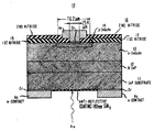
- the Figure shows a cross-sectional view of a typical confined-contact planar PIN photodiode with double nitride passivation.
- the structure, 10 is made up of an InP substrate, 11, within a thin buffer layer, 12 (2 to 6 ⁇ m thick) of n-type InP. This buffer layer is grown on the substrate by an epitaxial growth procedure such as liquid phase epitaxial growth.
- An active layer, 13, is made of n-type InGaAs grown by a liquid phase epitaxial procedure. The composition is adjusted to lattice match with the InP buffer layer (typical composition within ⁇ 10 mole percent In 0.53 Ga 0.47 As).
- a p type InGaAs region, 14, is made by diffusing zinc into the InGaAs as described below.
- the structure should not be exposed to excessively high temperatures for excessively long period of time before capping the active material (the InGaAs) with a dielectric or passivating material.
- the active material is capped with a first SiN x layer 15.
- a typical procedure is the use of a plasma chemical vapour deposition for nine minutes at 250 degrees C using a mixture of 2 percent SiH4 in argon metered into the reaction chamber at 20 cc/minute and nitrogen gas metered at the rate of 134 cc/minute.
- the temperature of the surface can usually be increased after deposition of a few tens of nanometres (e.g. 20 nanometres) of SiN x . Typically, the temperature is increased to between 300 and 400 degrees C.
- the structure may be exposed to higher temperatures, but it is preferred that time of exposure to the higher temperatures be limited when the capping substance is removed. Generally, such a high-temperature exposure is required during diffusion in the p-type region, 14, in the InGaAs.
- the p-type region 14 of the InGaAs is made by exposure to zinc vapour at a temperature below 600 degrees C (generally 500-600 degrees C with 550 ⁇ 20 degrees preferred) for a time under two hours (typically about one hour).
- a representative procedure is as follows. A window is opened in the first nitride layer by a standard positive photoresist procedure. An oxygen plasma etching procedure is used to remove the SiN x in the window. The remainder of the photoresist is then removed by standard procedures. There remains a hole in the SiN x with diameter typically of about 80 micrometres (3 mils).
- the doping procedure may be carried out in a variety of ways.
- a typical procedure involves diffusion from the vapour.
- Arsenic is usually included in the vapour to prevent loss of arsenic from the semiconductor surface.
- the wafer is sealed in a quartz ampoule containing the arsenic and zinc.
- the ampoule is heated to 550 degrees C for under two hours. The exact time depends on the thickness of the InGaAs layer and the amount of diffusion desired.
- the wafers are cooled and may be cleaned with a variety of solvents. Wafers are often tested at this point to determine the amount of leakage current.
- a second layer 16 of dielectric, e.g. SiN x is put down as indicated in the Figure.
- a hole is opened [generally about 25 micrometres (1 mil)] by conventional procedures as described above and chromium and gold put down (typically by electron beam evaporation). Typical thicknesses are for chromium about 100 nanometres and for gold about 1300 nanometres.
- the remainder of the structure is fabricated by conventional means.
- Photodiodes with active layers on phosphorus containing substrates fabricated as described typically have substantially lower dark currents than those fabricated at higher temperatures.
- PIN photodiodes can be regularly made with dark currents in the range from 5 to 20 nanoamperes at room temperature and 10 volts reverse bias.
Landscapes
- Light Receiving Elements (AREA)
- Formation Of Insulating Films (AREA)
Claims (9)
- Verfahren zur Herstellung eines III-V Verbindungshalbleiter-Fotodetektors umfassend das Ausbilden einer Anordnung mit einem Phosphor enthaltenden Substrat (11), wobei die Oberfläche des Substrates wenigsten teilweise mit einer aktiven, keinen Phosphor enthaltenden Verbindungshalbleiterschicht bedeckt ist, Abscheiden einer Siliciumnitrit-Abdeckschicht (15) auf der Oberfläche der aktiven Schicht (13) und Aussetzen der Anordnung einer Wärmebehandlung, wobei sich wenigstens ein Teil der Abdeckschicht an ihrer Stelle befindet,
dadurch gekennzeichnet, daß
die Abdeckschicht in einem Zwei-Stufen-Verfahren abgeschieden wird, umfassend:a) das Abscheiden einer Dicke von wenigstens 10 nm während die Temperatur der Anordnung unterhalb von 300 °C gehalten wird, undb) ferner Abscheiden bei einer Temperatur in dem Bereich von 300 °C bis 400 °C. - Verfahren nach Anspruch 1,
bei dem die Temperatur der Anordnung unter 250 °C gehalten wird, bis die Abdeckschicht (15) wenigstens 20 nm dick ist. - Verfahren nach Anspruch 1,
bei dem die Temperatur der Anordnung unter 250 °C gehalten wird, bis die Abdeckschicht (15) wenigstens 30 nm dick ist und unter 400 °C für eine zusätzliche Dicke bis zu 5 µm. - Verfahren nach einem der vorhergehenden Ansprüche, bei dem das Substrat (11) aus InP besteht, das Material der aktiven Schicht (13) n-leitend ist und aus InGaAs besteht und eine Pufferschicht (12) aus n-leitendem InP epitaxial auf das Substrat (11) und die aktive Schicht (13) abgeschieden wird.
- Verfahren nach einem der vorhergehenden Ansprüche, bei dem das Material der aktiven Schicht (13) eine Zusammensetzung von ± 10 mol% aus In0,53Ga0,47As.
- Verfahren nach einem der vorhergehenden Ansprüche, bei dem die Wärmebehandlung ein Diffusionsprozeß ist, bei dem ein Teil der Abdeckschicht (15) zur Freilegung eines Teils der Oberfläche der aktiven Schicht entfernt und ein Dotierstoff in den freigelegten Teil eindiffundiert wird.
- Verfahren nach Anspruch 6, bei dem die aktive Schicht (13) aus n-leitenden InGaAs besteht, der Dotierstoff Zink ist und die Diffusion ausgeführt wird, indem der freigelegte Teil in Kontakt mit einem Zink enthaltenden Dampf für weniger als zwei Stunden bei einer Temperatur zwischen 500 und 600 °C gebracht wird, um den freigelegten Teil p-leitend zu machen.
- Verfahren nach Anspruch 7, dadurch gekennzeichnet, daß Arsen in dem Dampf enthalten ist.
- Verfahren nach einem der vorhergehenden Ansprüche, dadurch gekennzeichnet, daß die Abdeckschicht durch eine chemische Plasma-Dampfabscheidung gebildet wird.
Applications Claiming Priority (2)
| Application Number | Priority Date | Filing Date | Title |
|---|---|---|---|
| US06/503,795 US4455351A (en) | 1983-06-13 | 1983-06-13 | Preparation of photodiodes |
| US503795 | 1983-06-13 |
Publications (4)
| Publication Number | Publication Date |
|---|---|
| EP0128724A2 EP0128724A2 (de) | 1984-12-19 |
| EP0128724A3 EP0128724A3 (en) | 1986-01-22 |
| EP0128724B1 EP0128724B1 (de) | 1990-03-07 |
| EP0128724B2 true EP0128724B2 (de) | 1994-01-12 |
Family
ID=24003542
Family Applications (1)
| Application Number | Title | Priority Date | Filing Date |
|---|---|---|---|
| EP84303761A Expired - Lifetime EP0128724B2 (de) | 1983-06-13 | 1984-06-05 | Herstellung von Photodioden |
Country Status (6)
| Country | Link |
|---|---|
| US (1) | US4455351A (de) |
| EP (1) | EP0128724B2 (de) |
| JP (1) | JPS609180A (de) |
| KR (1) | KR920003304B1 (de) |
| CA (1) | CA1199097A (de) |
| DE (1) | DE3481568D1 (de) |
Families Citing this family (18)
| Publication number | Priority date | Publication date | Assignee | Title |
|---|---|---|---|---|
| JPS5871589A (ja) * | 1981-10-22 | 1983-04-28 | シャープ株式会社 | 薄膜el素子 |
| DE3428951A1 (de) * | 1984-08-06 | 1986-02-13 | Leybold-Heraeus GmbH, 5000 Köln | Mit einer deckschicht aus gold oder einem goldhaltigen material ueberzogener dekorativer gebrauchsgegenstand und verfahren zu seiner herstellung |
| FR2571542B1 (fr) * | 1984-10-09 | 1987-01-23 | Labo Electronique Physique | Procede de realisation d'un dispositif semiconducteur incluant l'action de plasma |
| US4631219A (en) * | 1985-01-31 | 1986-12-23 | International Business Machines Corporation | Growth of bird's beak free semi-rox |
| US4705760A (en) * | 1986-01-16 | 1987-11-10 | Rca Corporation | Preparation of a surface for deposition of a passinating layer |
| US4794439A (en) * | 1987-03-19 | 1988-12-27 | General Electric Company | Rear entry photodiode with three contacts |
| JPS6472557A (en) * | 1987-09-11 | 1989-03-17 | Seiko Instr & Electronics | Image sensor |
| US5053837A (en) * | 1987-09-16 | 1991-10-01 | Sumitomo Electric Industries, Ltd. | Ingaas/inp type pin photodiodes |
| JPS6477942A (en) * | 1987-09-18 | 1989-03-23 | Fujitsu Ltd | Formation of protective film |
| US4876209A (en) * | 1988-01-06 | 1989-10-24 | U.S.C. | Method of making avalanche photodiode |
| DE4017870A1 (de) * | 1990-06-02 | 1991-12-05 | Standard Elektrik Lorenz Ag | Verfahren zur herstellung und passivierung von halbleiterbauelementen |
| SE470116B (sv) * | 1992-04-03 | 1993-11-08 | Asea Brown Boveri | Detektorkrets med en som detektor arbetande halvledardiod och en med dioden integrerad förstärkarkrets |
| JP3910817B2 (ja) * | 2000-12-19 | 2007-04-25 | ユーディナデバイス株式会社 | 半導体受光装置 |
| KR100454230B1 (ko) * | 2001-12-24 | 2004-10-26 | 광주과학기술원 | 유전체 특성이 개선된 InGaAs산화막의 형성방법 |
| US6780750B2 (en) * | 2002-01-08 | 2004-08-24 | Samsung Electronics Co. Ltd. | Photodiode for ultra high speed optical communication and fabrication method therefor |
| JP4956928B2 (ja) * | 2004-09-28 | 2012-06-20 | 日亜化学工業株式会社 | 半導体装置 |
| CN103762256B (zh) * | 2014-01-15 | 2016-03-02 | 华南理工大学 | 生长在Si衬底上的InGaAs薄膜及其制备方法 |
| CN106856211B (zh) * | 2016-11-28 | 2018-10-19 | 中国科学院上海微系统与信息技术研究所 | 一种Si(001)衬底上高In组分InGaAs探测器及其制备方法 |
Family Cites Families (5)
| Publication number | Priority date | Publication date | Assignee | Title |
|---|---|---|---|---|
| US4066037A (en) * | 1975-12-17 | 1978-01-03 | Lfe Corportion | Apparatus for depositing dielectric films using a glow discharge |
| SE7700229L (sv) * | 1976-01-22 | 1977-07-23 | Western Electric Co | Forfarande for beleggning av substrat genom utfellning fran ett plasma |
| JPS5436179A (en) * | 1977-08-26 | 1979-03-16 | Toshiba Corp | Forming method of nitride film |
| US4226667A (en) * | 1978-10-31 | 1980-10-07 | Bell Telephone Laboratories, Incorporated | Oxide masking of gallium arsenide |
| NL8001232A (nl) * | 1980-02-29 | 1981-10-01 | Philips Nv | Werkwijze voor het vervaardigen van een halfgeleiderinrichting. |
-
1983
- 1983-06-13 US US06/503,795 patent/US4455351A/en not_active Expired - Lifetime
-
1984
- 1984-05-10 CA CA000454018A patent/CA1199097A/en not_active Expired
- 1984-06-02 KR KR1019840003086A patent/KR920003304B1/ko not_active Expired
- 1984-06-05 DE DE8484303761T patent/DE3481568D1/de not_active Expired - Fee Related
- 1984-06-05 EP EP84303761A patent/EP0128724B2/de not_active Expired - Lifetime
- 1984-06-13 JP JP59120068A patent/JPS609180A/ja active Granted
Also Published As
| Publication number | Publication date |
|---|---|
| CA1199097A (en) | 1986-01-07 |
| DE3481568D1 (de) | 1990-04-12 |
| EP0128724B1 (de) | 1990-03-07 |
| JPH0586874B2 (de) | 1993-12-14 |
| KR920003304B1 (ko) | 1992-04-27 |
| KR850000809A (ko) | 1985-03-09 |
| JPS609180A (ja) | 1985-01-18 |
| US4455351A (en) | 1984-06-19 |
| EP0128724A2 (de) | 1984-12-19 |
| EP0128724A3 (en) | 1986-01-22 |
Similar Documents
| Publication | Publication Date | Title |
|---|---|---|
| EP0128724B2 (de) | Herstellung von Photodioden | |
| CA1292550C (en) | Epitaxial gallium arsenide semiconductor wafer and method of producing the same | |
| US4717631A (en) | Silicon oxynitride passivated semiconductor body and method of making same | |
| US6657194B2 (en) | Multispectral monolithic infrared focal plane array detectors | |
| US4634474A (en) | Coating of III-V and II-VI compound semiconductors | |
| WO2000052742A1 (en) | Epitaxially grown p-type diffusion source for photodiode fabrication | |
| US4514748A (en) | Germanium p-i-n photodetector on silicon substrate | |
| EP0179125A1 (de) | Anordnungen und verfahren unter verwendung organischer materialien | |
| EP0272833B1 (de) | Bauelemente und Bauelemente-Herstellung mit Borsilikatglass | |
| US5387796A (en) | Low leakage current photodetector arrays | |
| US4009058A (en) | Method of fabricating large area, high voltage PIN photodiode devices | |
| JP3602600B2 (ja) | SiO▲x▼層を含む製品及びその製品の作製法 | |
| US20030000454A1 (en) | Passivation of HgCdTe junction diode by annealing in Cd/Hg atmosphere | |
| US4801990A (en) | HgCdTe avalanche photodiode | |
| US5229321A (en) | Method of diffusing mercury into a crystalline semiconductor material including mercury | |
| US6787818B2 (en) | Diffused junction photodetector and fabrication technique | |
| US4862236A (en) | HgMnCdTe avalanche photodiode | |
| JPS58122721A (ja) | 化合物半導体への不純物拡散方法 | |
| JPS62172733A (ja) | 半導体基体 | |
| Camlibel et al. | Fabrication of Low Dark‐Current Planar Photodiodes Using an Open‐Tube Method for Zn Diffusion into InP and In0. 53Ga0. 47As | |
| EP0366886A1 (de) | Passivierte Verbindungshalbleiterstruktur | |
| CA1322040C (en) | Epitaxial gallium arsenide semiconductor wafer and method of producing the same | |
| JPS60173882A (ja) | 半導体装置 | |
| JPS6154619A (ja) | 砒化ガリウムp型伝導層の形成方法 | |
| McLevige | Annealing Studies of Beryllium in Gallium-Arsenide and Gallium Arsenide Phosphide. |
Legal Events
| Date | Code | Title | Description |
|---|---|---|---|
| PUAI | Public reference made under article 153(3) epc to a published international application that has entered the european phase |
Free format text: ORIGINAL CODE: 0009012 |
|
| AK | Designated contracting states |
Designated state(s): BE DE FR GB IT NL SE |
|
| PUAL | Search report despatched |
Free format text: ORIGINAL CODE: 0009013 |
|
| RHK1 | Main classification (correction) |
Ipc: H01L 21/324 |
|
| AK | Designated contracting states |
Designated state(s): BE DE FR GB IT NL SE |
|
| 17P | Request for examination filed |
Effective date: 19860625 |
|
| 17Q | First examination report despatched |
Effective date: 19880429 |
|
| GRAA | (expected) grant |
Free format text: ORIGINAL CODE: 0009210 |
|
| AK | Designated contracting states |
Kind code of ref document: B1 Designated state(s): BE DE FR GB IT NL SE |
|
| ITF | It: translation for a ep patent filed | ||
| REF | Corresponds to: |
Ref document number: 3481568 Country of ref document: DE Date of ref document: 19900412 |
|
| ET | Fr: translation filed | ||
| PLBI | Opposition filed |
Free format text: ORIGINAL CODE: 0009260 |
|
| 26 | Opposition filed |
Opponent name: STANDARD ELEKTRIK LORENZ AG, PATENT- UND LIZENZWE Effective date: 19901201 |
|
| NLR1 | Nl: opposition has been filed with the epo |
Opponent name: STANDARD ELEKTRIK LORENZ AG. |
|
| ITTA | It: last paid annual fee | ||
| PLAB | Opposition data, opponent's data or that of the opponent's representative modified |
Free format text: ORIGINAL CODE: 0009299OPPO |
|
| R26 | Opposition filed (corrected) |
Opponent name: ALCATEL SEL AKTIENGESELLSCHAFT Effective date: 19901201 |
|
| NLXE | Nl: other communications concerning ep-patents (part 3 heading xe) |
Free format text: PAT.BUL.06/91 CORR.:ALCATEL SEL AG |
|
| PUAH | Patent maintained in amended form |
Free format text: ORIGINAL CODE: 0009272 |
|
| STAA | Information on the status of an ep patent application or granted ep patent |
Free format text: STATUS: PATENT MAINTAINED AS AMENDED |
|
| 27A | Patent maintained in amended form |
Effective date: 19940112 |
|
| AK | Designated contracting states |
Kind code of ref document: B2 Designated state(s): BE DE FR GB IT NL SE |
|
| NLR2 | Nl: decision of opposition | ||
| ET3 | Fr: translation filed ** decision concerning opposition | ||
| ITF | It: translation for a ep patent filed | ||
| NLR3 | Nl: receipt of modified translations in the netherlands language after an opposition procedure | ||
| EAL | Se: european patent in force in sweden |
Ref document number: 84303761.5 |
|
| PGFP | Annual fee paid to national office [announced via postgrant information from national office to epo] |
Ref country code: BE Payment date: 19990329 Year of fee payment: 16 |
|
| PG25 | Lapsed in a contracting state [announced via postgrant information from national office to epo] |
Ref country code: BE Free format text: LAPSE BECAUSE OF NON-PAYMENT OF DUE FEES Effective date: 20000630 |
|
| BERE | Be: lapsed |
Owner name: AMERICAN TELEPHONE AND TELEGRAPH CY Effective date: 20000630 |
|
| PGFP | Annual fee paid to national office [announced via postgrant information from national office to epo] |
Ref country code: SE Payment date: 20010321 Year of fee payment: 18 |
|
| PGFP | Annual fee paid to national office [announced via postgrant information from national office to epo] |
Ref country code: NL Payment date: 20010529 Year of fee payment: 18 |
|
| PGFP | Annual fee paid to national office [announced via postgrant information from national office to epo] |
Ref country code: DE Payment date: 20010629 Year of fee payment: 18 |
|
| REG | Reference to a national code |
Ref country code: GB Ref legal event code: IF02 |
|
| PG25 | Lapsed in a contracting state [announced via postgrant information from national office to epo] |
Ref country code: SE Free format text: LAPSE BECAUSE OF NON-PAYMENT OF DUE FEES Effective date: 20020606 |
|
| PG25 | Lapsed in a contracting state [announced via postgrant information from national office to epo] |
Ref country code: NL Free format text: LAPSE BECAUSE OF NON-PAYMENT OF DUE FEES Effective date: 20030101 Ref country code: DE Free format text: LAPSE BECAUSE OF NON-PAYMENT OF DUE FEES Effective date: 20030101 |
|
| EUG | Se: european patent has lapsed | ||
| NLV4 | Nl: lapsed or anulled due to non-payment of the annual fee |
Effective date: 20030101 |
|
| PGFP | Annual fee paid to national office [announced via postgrant information from national office to epo] |
Ref country code: FR Payment date: 20030618 Year of fee payment: 20 |
|
| PGFP | Annual fee paid to national office [announced via postgrant information from national office to epo] |
Ref country code: GB Payment date: 20030714 Year of fee payment: 20 |
|
| PG25 | Lapsed in a contracting state [announced via postgrant information from national office to epo] |
Ref country code: GB Free format text: LAPSE BECAUSE OF EXPIRATION OF PROTECTION Effective date: 20040604 |
|
| REG | Reference to a national code |
Ref country code: GB Ref legal event code: PE20 |