EP0273123A2 - Amplificateur opérationnel utilisant des suiveurs à transistors JFET - Google Patents
Amplificateur opérationnel utilisant des suiveurs à transistors JFET Download PDFInfo
- Publication number
- EP0273123A2 EP0273123A2 EP87115292A EP87115292A EP0273123A2 EP 0273123 A2 EP0273123 A2 EP 0273123A2 EP 87115292 A EP87115292 A EP 87115292A EP 87115292 A EP87115292 A EP 87115292A EP 0273123 A2 EP0273123 A2 EP 0273123A2
- Authority
- EP
- European Patent Office
- Prior art keywords
- source
- jfet
- coupled
- current
- dss
- Prior art date
- Legal status (The legal status is an assumption and is not a legal conclusion. Google has not performed a legal analysis and makes no representation as to the accuracy of the status listed.)
- Granted
Links
- 230000008878 coupling Effects 0.000 claims 7
- 238000010168 coupling process Methods 0.000 claims 7
- 238000005859 coupling reaction Methods 0.000 claims 7
- 238000010586 diagram Methods 0.000 description 2
- 239000003990 capacitor Substances 0.000 description 1
- 238000000034 method Methods 0.000 description 1
- 238000009966 trimming Methods 0.000 description 1
Images
Classifications
-
- H—ELECTRICITY
- H03—ELECTRONIC CIRCUITRY
- H03F—AMPLIFIERS
- H03F3/00—Amplifiers with only discharge tubes or only semiconductor devices as amplifying elements
- H03F3/45—Differential amplifiers
-
- H—ELECTRICITY
- H03—ELECTRONIC CIRCUITRY
- H03F—AMPLIFIERS
- H03F3/00—Amplifiers with only discharge tubes or only semiconductor devices as amplifying elements
- H03F3/45—Differential amplifiers
- H03F3/45071—Differential amplifiers with semiconductor devices only
- H03F3/45076—Differential amplifiers with semiconductor devices only characterised by the way of implementation of the active amplifying circuit in the differential amplifier
- H03F3/4508—Differential amplifiers with semiconductor devices only characterised by the way of implementation of the active amplifying circuit in the differential amplifier using bipolar transistors as the active amplifying circuit
- H03F3/45085—Long tailed pairs
-
- H—ELECTRICITY
- H03—ELECTRONIC CIRCUITRY
- H03F—AMPLIFIERS
- H03F2203/00—Indexing scheme relating to amplifiers with only discharge tubes or only semiconductor devices as amplifying elements covered by H03F3/00
- H03F2203/45—Indexing scheme relating to differential amplifiers
- H03F2203/45612—Indexing scheme relating to differential amplifiers the IC comprising one or more input source followers as input stages in the IC
-
- H—ELECTRICITY
- H03—ELECTRONIC CIRCUITRY
- H03F—AMPLIFIERS
- H03F2203/00—Indexing scheme relating to amplifiers with only discharge tubes or only semiconductor devices as amplifying elements covered by H03F3/00
- H03F2203/45—Indexing scheme relating to differential amplifiers
- H03F2203/45631—Indexing scheme relating to differential amplifiers the LC comprising one or more capacitors, e.g. coupling capacitors
-
- H—ELECTRICITY
- H03—ELECTRONIC CIRCUITRY
- H03F—AMPLIFIERS
- H03F2203/00—Indexing scheme relating to amplifiers with only discharge tubes or only semiconductor devices as amplifying elements covered by H03F3/00
- H03F2203/45—Indexing scheme relating to differential amplifiers
- H03F2203/45674—Indexing scheme relating to differential amplifiers the LC comprising one current mirror
-
- H—ELECTRICITY
- H03—ELECTRONIC CIRCUITRY
- H03F—AMPLIFIERS
- H03F2203/00—Indexing scheme relating to amplifiers with only discharge tubes or only semiconductor devices as amplifying elements covered by H03F3/00
- H03F2203/45—Indexing scheme relating to differential amplifiers
- H03F2203/45684—Indexing scheme relating to differential amplifiers the LC comprising one or more buffers or driving stages not being of the emitter respectively source follower type, between the output of the dif amp and the output stage
Definitions
- This invention relates generally to operational amplifiers, and more particularly, to an operational amplifier utilizing JFET followers each of which is driven by a current source generating a current which is proportional to the saturation current I DSS of its respective JFET follower and which tracks its respective I DSS over temperature.
- an amplifier having first and second inputs, comprising first and second emitter coupled transistors.
- Current mirror means is coupled to the collectors of said first and second transistor.
- a first JFET has a source coupled to the base of said first transistor, a gate coupled to the first input, and has a first I DSS .
- a second JFET has a source coupled to the base of the second transistor, a gate coupled to said second input, and has a second I DSS .
- First means is coupled to the source of the first JFET for supplying a first current thereto substantially equal to its I DSS ; and second means coupled to the source of the second JFET for supplying a second current thereto substantially equal to its I DSS .
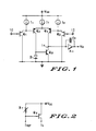
- the operational amplifier shown in FIG. 1 includes a pair of emitter coupled PNP transistors Q3 and Q4 each of which have their collectors coupled to a current mirror circuit comprised of diode means D1 and NPN transistor Q5. That is, the collector of PNP transistor Q3 is coupled to the anode of diode D1 and to the base of transistor Q5. The collector of transistor Q4 is coupled to the collector of transistor Q5. Both the cathode of diode D1 and emitter of transistor Q5 are coupled to a source of supply voltage (e.g. ground). The tail current required by this circuitry is provided by a current source I t coupled between the emitters of transistors Q3 and Q4 and another source of supply voltage (V CC ).
- V CC source of supply voltage
- the base electrodes of transistors Q3 and Q4 are coupled respectively to the source electrodes of junction field-effect-transistors (JFETs) Q1 and Q2 respectively each of which have a drain coupled to ground.
- Q1 has a gate terminal coupled to a first input terminal 10
- Q2 has a gate coupled to a second input terminal 12.
- the remainder of the operational amplifier represented by amplifier A1 having an input coupled to the collector junction of transistors Q4 and Q5, the output of which (V0) represents the amplifier output, and a compensation capacitor C c coupled in parallel with amplifier A1).
- current sources I1 and I2 are provided for driving junction field-effect-transistors Q1 and Q2 respectively, and it is the nature of these current sources and their relationship to the circuit as a whole which renders the circuit shown in FIG. 1 inventive.
- V gs The gate to source voltage (V gs ) of a JFET may be represented as where V p is a pinch-off voltage of the JFET, I D is the drain current and I DSS represents the JFET's drain current when its gate and source are shorted.
- V os V gsQ2 - V gsQ1 (2)
- dI2/dT dI DSSQ2 /dT
- dI1/dT dI DSSQ1 /dT
- the rate of change of the offset voltage with respect to temperature may be represented as It can be seen that if I2 is substantially equal to I DSSQ2 and I1 is substantially equal to I DSSQ1 , then both the offset voltage V os and the rate of change of V os with temperature (dV os /dT) equals zero. That is, by trimming the offset voltage to zero, dV os /dT is also automatically trimmed to zero.
- Current sources I1 and I2 may be generated by the circuit shown in FIG. 2 which is described in copending U.S. Application Serial No. SC05986C entitled TRIMMABLE CURRENT SOURCE and assigned to the assignee of the present invention.
- each inventive current source comprises a JFET Q6 having a source coupled to a source of supply voltage V CC and having a drain at which the required current I1, I2 is made available.
- the gate of Q6 is coupled via a trimmable resistor R T to the source of supply V CC .
- the gate is also coupled to the source of a reference current I REF .
- the reference current I REF is equal to V P /R where V P is the pinch-off voltage of a JFET and R is some resistance.
- I d I DSS (1 + V p R T /V p R)2 (8)
- I d I DSS (1 + R T /R)2 (9)
- the circuit shown in FIG. 2 when driven by a reference current equal to V P /R produces a current I d which is proportional to I DSS and trimmable and one which has a temperature coefficient which is proportional to that of I DSS .
- the operational amplifier shown in FIG. 1 operates in the well known manner. That is, when the voltage at terminal 10 is greater than that at terminal 12, JFET Q1 turns on causing the voltage at the base of transistor Q3 to fall thus turning it on. The current flowing in the collector of Q3 will thus be greater than that flowing in the collector of Q4. Since the current mirror action of diode D1 and transistor Q5 will attempt to mirror the current flowing in the collector of Q3 in the collector of Q5, the voltage at node 14 which is applied to the amplifier's output stage will fall. In contrast, should the potential at input terminal 10 be less than that at terminal 12, JFET Q2 will turn on causing transistor Q4 to conduct harder than transistor Q3. In this case, the current being mirrored to the collector of transistor Q5 is less than that flowing in the collector of transistor Q4 and the voltage at node 14 will rise.
Landscapes
- Engineering & Computer Science (AREA)
- Power Engineering (AREA)
- Amplifiers (AREA)
Applications Claiming Priority (2)
| Application Number | Priority Date | Filing Date | Title |
|---|---|---|---|
| US06/947,127 US4713626A (en) | 1986-12-29 | 1986-12-29 | Operational amplifier utilizing JFET followers |
| US947127 | 1992-09-17 |
Publications (3)
| Publication Number | Publication Date |
|---|---|
| EP0273123A2 true EP0273123A2 (fr) | 1988-07-06 |
| EP0273123A3 EP0273123A3 (en) | 1989-03-08 |
| EP0273123B1 EP0273123B1 (fr) | 1992-04-15 |
Family
ID=25485565
Family Applications (1)
| Application Number | Title | Priority Date | Filing Date |
|---|---|---|---|
| EP87115292A Expired - Lifetime EP0273123B1 (fr) | 1986-12-29 | 1987-10-19 | Amplificateur opérationnel utilisant des suiveurs à transistors JFET |
Country Status (6)
| Country | Link |
|---|---|
| US (1) | US4713626A (fr) |
| EP (1) | EP0273123B1 (fr) |
| JP (1) | JPS63169805A (fr) |
| KR (1) | KR880008516A (fr) |
| DE (1) | DE3778328D1 (fr) |
| HK (1) | HK89695A (fr) |
Families Citing this family (5)
| Publication number | Priority date | Publication date | Assignee | Title |
|---|---|---|---|---|
| JP2693501B2 (ja) * | 1988-07-29 | 1997-12-24 | 株式会社東芝 | 差動増幅回路 |
| JPH02113787A (ja) * | 1988-10-24 | 1990-04-25 | Matsushita Electric Ind Co Ltd | フレーム間デインターリーブ切換回路 |
| US6731273B2 (en) * | 2000-06-27 | 2004-05-04 | Semiconductor Energy Laboratory Co., Ltd. | Level shifter |
| US7052706B2 (en) * | 2001-06-08 | 2006-05-30 | Nostrum Pharmaceuticals, Inc. | Control release formulation containing a hydrophobic material as the sustained release agent |
| JP5390932B2 (ja) * | 2009-05-14 | 2014-01-15 | セミコンダクター・コンポーネンツ・インダストリーズ・リミテッド・ライアビリティ・カンパニー | 電源回路 |
Family Cites Families (3)
| Publication number | Priority date | Publication date | Assignee | Title |
|---|---|---|---|---|
| US3703650A (en) * | 1971-09-16 | 1972-11-21 | Signetics Corp | Integrated circuit with temperature compensation for a field effect transistor |
| JPS6133709Y2 (fr) * | 1977-11-24 | 1986-10-02 | ||
| US4517524A (en) * | 1983-07-01 | 1985-05-14 | Motorola, Inc. | High frequency operational amplifier |
-
1986
- 1986-12-29 US US06/947,127 patent/US4713626A/en not_active Expired - Lifetime
-
1987
- 1987-10-19 EP EP87115292A patent/EP0273123B1/fr not_active Expired - Lifetime
- 1987-10-19 DE DE8787115292T patent/DE3778328D1/de not_active Expired - Lifetime
- 1987-12-09 JP JP62311794A patent/JPS63169805A/ja active Pending
- 1987-12-29 KR KR1019870015199A patent/KR880008516A/ko not_active Withdrawn
-
1995
- 1995-06-08 HK HK89695A patent/HK89695A/en not_active IP Right Cessation
Also Published As
| Publication number | Publication date |
|---|---|
| DE3778328D1 (de) | 1992-05-21 |
| KR880008516A (ko) | 1988-08-31 |
| HK89695A (en) | 1995-06-16 |
| EP0273123B1 (fr) | 1992-04-15 |
| EP0273123A3 (en) | 1989-03-08 |
| JPS63169805A (ja) | 1988-07-13 |
| US4713626A (en) | 1987-12-15 |
Similar Documents
| Publication | Publication Date | Title |
|---|---|---|
| US4399399A (en) | Precision current source | |
| EP0276670B1 (fr) | Circuit rapide décaleur de tension, indépendant de l'alimentation | |
| JPS61230411A (ja) | 電気回路 | |
| KR0136875B1 (ko) | 전압-전류 변환기 | |
| US4636744A (en) | Front end of an operational amplifier | |
| US4636743A (en) | Front end stage of an operational amplifier | |
| EP0209987B1 (fr) | Amplificateur tampon à gain unité | |
| US4524318A (en) | Band gap voltage reference circuit | |
| US4567444A (en) | Current mirror circuit with control means for establishing an input-output current ratio | |
| US4574233A (en) | High impedance current source | |
| EP0155720B1 (fr) | Dispositif de source de courant en cascade | |
| US4004245A (en) | Wide common mode range differential amplifier | |
| EP0044339B1 (fr) | Circuit miroir de courant | |
| EP0273123A2 (fr) | Amplificateur opérationnel utilisant des suiveurs à transistors JFET | |
| US4194166A (en) | Differential amplifier with a current mirror circuit | |
| US4398160A (en) | Current mirror circuits with field effect transistor feedback | |
| EP0156410B1 (fr) | Montage amplificateur | |
| US5128564A (en) | Input bias current compensation for a comparator | |
| US4724397A (en) | Trimmable differential amplifier having a zero temperature coefficient offset voltage and method | |
| KR20010034225A (ko) | 전류 미러 회로 | |
| EP0157447B1 (fr) | Amplificateur différentiel | |
| EP0456127B1 (fr) | Amplificateur | |
| US4317082A (en) | Current mirror circuit | |
| US4736126A (en) | Trimmable current source | |
| US4714894A (en) | Operational amplifier |
Legal Events
| Date | Code | Title | Description |
|---|---|---|---|
| PUAI | Public reference made under article 153(3) epc to a published international application that has entered the european phase |
Free format text: ORIGINAL CODE: 0009012 |
|
| AK | Designated contracting states |
Kind code of ref document: A2 Designated state(s): DE FR GB |
|
| PUAL | Search report despatched |
Free format text: ORIGINAL CODE: 0009013 |
|
| AK | Designated contracting states |
Kind code of ref document: A3 Designated state(s): DE FR GB |
|
| 17P | Request for examination filed |
Effective date: 19890413 |
|
| 17Q | First examination report despatched |
Effective date: 19901217 |
|
| GRAA | (expected) grant |
Free format text: ORIGINAL CODE: 0009210 |
|
| AK | Designated contracting states |
Kind code of ref document: B1 Designated state(s): DE FR GB |
|
| PG25 | Lapsed in a contracting state [announced via postgrant information from national office to epo] |
Ref country code: FR Effective date: 19920415 |
|
| REF | Corresponds to: |
Ref document number: 3778328 Country of ref document: DE Date of ref document: 19920521 |
|
| EN | Fr: translation not filed | ||
| PLBE | No opposition filed within time limit |
Free format text: ORIGINAL CODE: 0009261 |
|
| STAA | Information on the status of an ep patent application or granted ep patent |
Free format text: STATUS: NO OPPOSITION FILED WITHIN TIME LIMIT |
|
| 26N | No opposition filed | ||
| PGFP | Annual fee paid to national office [announced via postgrant information from national office to epo] |
Ref country code: GB Payment date: 19970930 Year of fee payment: 11 |
|
| PGFP | Annual fee paid to national office [announced via postgrant information from national office to epo] |
Ref country code: DE Payment date: 19971023 Year of fee payment: 11 |
|
| PG25 | Lapsed in a contracting state [announced via postgrant information from national office to epo] |
Ref country code: GB Free format text: LAPSE BECAUSE OF NON-PAYMENT OF DUE FEES Effective date: 19981019 |
|
| GBPC | Gb: european patent ceased through non-payment of renewal fee |
Effective date: 19981019 |
|
| PG25 | Lapsed in a contracting state [announced via postgrant information from national office to epo] |
Ref country code: DE Free format text: LAPSE BECAUSE OF NON-PAYMENT OF DUE FEES Effective date: 19990803 |