EP0273665A2 - Anordnung, um optische Speicheranlagen des Wormtyps scheinbar neuschreibbar zu machen - Google Patents
Anordnung, um optische Speicheranlagen des Wormtyps scheinbar neuschreibbar zu machen Download PDFInfo
- Publication number
- EP0273665A2 EP0273665A2 EP87311230A EP87311230A EP0273665A2 EP 0273665 A2 EP0273665 A2 EP 0273665A2 EP 87311230 A EP87311230 A EP 87311230A EP 87311230 A EP87311230 A EP 87311230A EP 0273665 A2 EP0273665 A2 EP 0273665A2
- Authority
- EP
- European Patent Office
- Prior art keywords
- storage
- worm
- data
- storage means
- cache
- Prior art date
- Legal status (The legal status is an assumption and is not a legal conclusion. Google has not performed a legal analysis and makes no representation as to the accuracy of the status listed.)
- Withdrawn
Links
Images


Classifications
-
- G—PHYSICS
- G11—INFORMATION STORAGE
- G11B—INFORMATION STORAGE BASED ON RELATIVE MOVEMENT BETWEEN RECORD CARRIER AND TRANSDUCER
- G11B20/00—Signal processing not specific to the method of recording or reproducing; Circuits therefor
- G11B20/10—Digital recording or reproducing
- G11B20/12—Formatting, e.g. arrangement of data block or words on the record carriers
- G11B20/1217—Formatting, e.g. arrangement of data block or words on the record carriers on discs
-
- G—PHYSICS
- G06—COMPUTING OR CALCULATING; COUNTING
- G06F—ELECTRIC DIGITAL DATA PROCESSING
- G06F12/00—Accessing, addressing or allocating within memory systems or architectures
- G06F12/02—Addressing or allocation; Relocation
- G06F12/08—Addressing or allocation; Relocation in hierarchically structured memory systems, e.g. virtual memory systems
- G06F12/0802—Addressing of a memory level in which the access to the desired data or data block requires associative addressing means, e.g. caches
- G06F12/0866—Addressing of a memory level in which the access to the desired data or data block requires associative addressing means, e.g. caches for peripheral storage systems, e.g. disk cache
-
- G—PHYSICS
- G06—COMPUTING OR CALCULATING; COUNTING
- G06F—ELECTRIC DIGITAL DATA PROCESSING
- G06F12/00—Accessing, addressing or allocating within memory systems or architectures
- G06F12/02—Addressing or allocation; Relocation
- G06F12/08—Addressing or allocation; Relocation in hierarchically structured memory systems, e.g. virtual memory systems
- G06F12/12—Replacement control
- G06F12/121—Replacement control using replacement algorithms
- G06F12/126—Replacement control using replacement algorithms with special data handling, e.g. priority of data or instructions, handling errors or pinning
-
- G—PHYSICS
- G11—INFORMATION STORAGE
- G11B—INFORMATION STORAGE BASED ON RELATIVE MOVEMENT BETWEEN RECORD CARRIER AND TRANSDUCER
- G11B20/00—Signal processing not specific to the method of recording or reproducing; Circuits therefor
- G11B20/10—Digital recording or reproducing
- G11B2020/10898—Overwriting or replacing recorded data
- G11B2020/10907—Overwriting or replacing recorded data using pseudo-overwriting, i.e. virtually or logically overwriting data on WORM media by remapping recorded blocks to alternate areas
-
- G—PHYSICS
- G11—INFORMATION STORAGE
- G11B—INFORMATION STORAGE BASED ON RELATIVE MOVEMENT BETWEEN RECORD CARRIER AND TRANSDUCER
- G11B2220/00—Record carriers by type
- G11B2220/40—Combinations of multiple record carriers
- G11B2220/45—Hierarchical combination of record carriers, e.g. HDD for fast access, optical discs for long term storage or tapes for backup
- G11B2220/455—Hierarchical combination of record carriers, e.g. HDD for fast access, optical discs for long term storage or tapes for backup said record carriers being in one device and being used as primary and secondary/backup media, e.g. HDD-DVD combo device, or as source and target media, e.g. PC and portable player
Definitions
- This invention relates to method and apparatus to make a write once read many optical storage device appear to be rewritable.
- WORM Write Once Read Many
- an object of the present invention to provide a system to allow use of WORM media with ease approaching conventional storage, the system described herein providing a generally applicable solution for simplified, economical integration of WORM storage systems into existing computer systems, in a manner transparent to application software and at reduced cost and development time.
- an apparatus for increasing the utility of a Write Once Read Many (WORM) storage medium includes cache storage means and caching system controller means operatively coupled to the cache and WORM storage means for determining where in the cache storage means new data is to be written and which data currently stored therein is to be transferred to the WORM storage means to make room for the new data. In this way, the number of write operations to the WORM storage means is minimized and its efficiency increased.
- WORM Write Once Read Many
- the cache and WORM storage means comprise magnetic and optical storage subsystems, respectively.
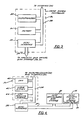
- FIG. 1 depicts in block schematic form a conventional computer system 10, which may be thought of as being subdivided internally into at least two functionally separate parts identified in FIG. 1 as applications software portion 12 and operating system software 14.
- the applications software performs for the user the "useful" tasks, e.g., data analysis, which produce the desired end result.
- the operating system software is a utility program which performs "housekeeping" functions, such as timely storage and retrieval of data needed to execute the applications software.
- the operating system includes a manager portion 16 and a disk driver portion 18 which communicates through a computer-specific interface 20 with a magnetic disk storage 22, which may be in the form frequently referred to as "hard disk.”
- storage 22 may be any other conventional magnetic storage medium, such as tape.
- Interface 20 is of known design but is specific to the particular computer 10 and magnetic disk storage 22.
- FIG. 2 depicts a block-schematic diagram of the system comprised of computer 10, interface 20 through which the computer communicates bidirectionally with an optical disk subsystem generally designated 24.
- the optical disk subsystem is made up of a caching system controller 26 which is linked bidirectionally with interface 20 and a Small Computer System Interface (SCSI) magnetic disk storage 28 and a SCSI optical disk storage (WORM) 30.
- SCSI Small Computer System Interface
- WORM SCSI optical disk storage
- magnetic storage 28 and optical storage 30 may comprise conventional devices, each including the necessary associated subsystems, as appropriate.
- optical disk subsystem 24 remains unchanged regardless of the type of computer 10 being used.
- a different computer interface 20 is, however, needed to render the computer compatible with the caching system controller. In this way, the optical disk subsystem is easily and economically integratable into any computer system without the need to modify the operating system software.
- the caching system controller includes a microprocessor 32 which communicates on a standard microprocessor bus 34 with a memory 36 and through a Small Computer System Interface 38 with a SCSI magnetic and SCSI optical storage 28 and 30, respectively. Microprocessor 32 is also linked by means of bus 34 to computer 10 through interface 20.
- Memory 36 is organized as shown in FIG. 4.
- Memory 36 includes Content Addressable Memory (CAM) 40, scrub system 42 and Least Recently Written (LRW) tracking system 44, all of which are linked through bus 34.
- CAM Content Addressable Memory
- LRW Least Recently Written
- FIG. 4 optical disk storage 30 and a magnetic disk storage 28, where cache memory 29 resides, as will be more fully described hereinafter.
- Optical disk storage 30 and magnetic disk storage 28 communicate with the rest of the system thorugh SCSI interface 38 on a bus 39.
- Magnetic disk storage 28 and optical disk storage 30 are functionally combined through caching system controller 26 to appear in operation as a single physical unit. This single unit has, as a whole, the attributes of being rewritable.
- FIG. 5 illustrates another embodiment of the inventive system similar to that disclosed with reference to FIGS. 3 and 4, but in which caching controller system 26 is connected to bus 39, on the "other side" of SCSI interface 38 (FIG. 4).
- Memory 36 remains configured as shown in FIG. 4, except that the bus connections are changed to those shown in FIG. 5. Operationally the system remains the same.
- the optical device is made to appear to be writable many times. This is accomplished by organizing operation of the above-described system in two parts.
- the first part includes cache storage 29 (FIG. 4) for data being written.
- the second part is a replacement mapping or some other conventional method for reassigning information to a new area.
- the second part is performed in scrub system 42.
- the first part is somewhat analogous to the memory caches of the past. In much the same manner that such caches could make a slower memory appear to approach the speed of a conventional memory, so too, a write cache can be used to make the write-once optical subsystem appear to approach the writability of a conventional storage subsystem.
- FIG. 6 shows, by way of example, three units of storage 50-52 of an optical storage device each having address locations designated by numerals 53-55.
- units 50 and 51 contain previously transferred data which has become obsolete.
- Unit 52 contains valid data.
- a request for information directed to address 53 results in a transfer to address 54 (unit 51) and from there to unit 52 which, finally, contains valid data.
- address 55 will be updated to the address of the next unit which would contain the then valid data.
- Such a "link-list" can be, of course, expanded as needed.
- cache memory 29 An important part of the inventive system is cache memory 29 (FIG. 4).
- the task of the cache is to reduce the number of accesses (both read and write) to a larger and slower storage medium.
- the cache storage is faster and the result is that the larger, slower storage will appear to approach the speed of the smaller, faster cache storage.
- the task of cache memory is not to speed up access time, but to reduce and/or eliminate the necessity to rewrite data on the optical disk. This acts to increase the versatility of the WORM storage and makes it appear as being rewritable.
- An additional benefit is increase the efficiency of the WORM medium due to inherent higher speed of magnetic disk storage 28, which contains cache memory 29.
- the described system uses the Content Addressable Memory (CAM) 40 (FIG. 4) to keep track of what and where information is in cache storage 29 and also what is not in cache storage and therefore may be on the optical media 30. Only write operations to the optical system result in a modification/entry to the cache system CAM. What information is kept in cache and what information gets through to the optical storage system is controlled by a modified Least Recently Used (LRU) algorithm. In this system all write entries go to cache storage 29 and remain there until they become the least recently written information, when they become eligible to be written to the optical storage system. Because the goal is to cache the "write" operation, the LRU algorithm is modified to a Least Recently Written (LWR).
- LWR Least Recently Written
- the LRW tracking system utilizes a strategy which selects which sectors of the subsystem need to remain in cache storage and which are the best choice for retirement to optical disk storage.
- those cache storage sectors which have not been written for the longest time will be the first to be written to optical disk storage.
- those sectors which have been written most recently will remain in cache storage.
- the decision is made on heuristic that the recent past is a good indicator of the near future. That is, those sectors which have not been written for the longest time are the most likely not to be written in the near future and, therefore, are good candidates for transfer to the optical storage system.
- the approximation of a LRW is based on the longest unwritten--first out.
- the sector being written to the optical storage subsystem will be cached in the magnetic disk at the location of the sector which has been unwritten for the longest time or one which has never been used.
- FIG. 7 depicts in simplified form five locations 58-62 in cache storage 29.
- LRW tracking system 44 (FIG. 4) will be briefly described with reference to FIG. 7 which depicts in simplified form five locations 58-62 in cache storage 29.
- inquiries are made as to whether cache storage is full and whether data contained therein is valid. If the cache is not full, the write operation places data in the empty area. Similarly, if there is invalid (obsolete) data in cache storage the new data replaces the old data. If neither of these two conditions exists and a write operation must be performed, a determination is made as to which of the data in locations 58-62 is the oldest (least recently written). This old data is transferred to optical WORM storage and the new data placed in its location in cache storage.
- the LRW of the new data is designated as the most recently written and the address of the new data entered in CAM 40. Thus, if the new data is written into location 62, any subsequent data written would go to one of locations 58-61, depending on which is then the "oldest.” This process is repeated continuously, so that only the oldest valid data is transferred to the optical disk.
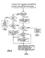
- FIGURE 8 illustrates in flow-chart form the sequence of operation of the described system and with reference to which a more detailed description will be made.
- the sequence of operation is initiated by receipt from computer 10 of either an address and information to be written or an address to be read from a WORM optical storage system.
- the next step in the functional sequence is a search conducted under direction of microprocessor 32 (FIG. 3) of the CAM memory 40 (FIG. 4) to determine whether the address sought is in cache storage 29 (HIT). Depending on what the result of the search is, the procedure splits into two logic paths.
- the address is computed.
- a "read” determination results in data being read from cache storage and the sequence terminates.
- a "write” determination requires replacement of old data in cache storage with the new data to be written.
- cache storage 29 resides on magnetic disk storage 28 (FIG. 4) so that all new data written into storage is actually written on magnetic medium which is reusable. This avoids writing all data into optical WORM device, as would be conventionally done in past systems, and thus avoids drawbacks associated therewith.
- the result of the CAM search is a Miss and data is to be written, then (if the cache storage is full) the oldest valid data in cache storage ismoved from cache storage to optical WORM storage, the new data/address is written into the emptied cache and CAM, and the LRW of the new entry is updated to be most recent. In this manner, only the data with the oldest LWR index is written into optical WORM storage, and conversely it serves to keep the most frequently used data in the magnetic cache storage.
Landscapes
- Engineering & Computer Science (AREA)
- Theoretical Computer Science (AREA)
- Physics & Mathematics (AREA)
- General Engineering & Computer Science (AREA)
- General Physics & Mathematics (AREA)
- Signal Processing (AREA)
- Memory System Of A Hierarchy Structure (AREA)
- Information Retrieval, Db Structures And Fs Structures Therefor (AREA)
- Signal Processing For Digital Recording And Reproducing (AREA)
Applications Claiming Priority (2)
| Application Number | Priority Date | Filing Date | Title |
|---|---|---|---|
| US27587A | 1987-01-02 | 1987-01-02 | |
| US275 | 1987-01-02 |
Publications (2)
| Publication Number | Publication Date |
|---|---|
| EP0273665A2 true EP0273665A2 (de) | 1988-07-06 |
| EP0273665A3 EP0273665A3 (de) | 1990-06-06 |
Family
ID=21690766
Family Applications (1)
| Application Number | Title | Priority Date | Filing Date |
|---|---|---|---|
| EP87311230A Withdrawn EP0273665A3 (de) | 1987-01-02 | 1987-12-21 | Anordnung, um optische Speicheranlagen des Wormtyps scheinbar neuschreibbar zu machen |
Country Status (2)
| Country | Link |
|---|---|
| EP (1) | EP0273665A3 (de) |
| JP (1) | JPH0650482B2 (de) |
Cited By (18)
| Publication number | Priority date | Publication date | Assignee | Title |
|---|---|---|---|---|
| EP0357464A3 (de) * | 1988-09-02 | 1991-03-20 | Matsushita Electric Industrial Co., Ltd. | Informationsaufzeichnungs- und -wiedergabegerät mit optischen Speicherplatten |
| EP0363135A3 (de) * | 1988-10-06 | 1992-01-15 | Alphatronix Inc. | System und Verfahren zur Ausführung von Übertragungsoperationen für Multi-Bestände |
| EP0510832A1 (de) * | 1991-04-22 | 1992-10-28 | International Business Machines Corporation | Cachespeicherseitenersetzung mit LIFO-Auswechselung |
| EP0667579A1 (de) * | 1994-02-09 | 1995-08-16 | Ballard Synergy Corporation | Cache-Speicher für optische Speichervorrichtung |
| EP0665499A3 (de) * | 1994-01-27 | 1996-03-27 | Int Computers Ltd | Hierarchisches Datenspeichersystem. |
| US5584007A (en) * | 1994-02-09 | 1996-12-10 | Ballard Synergy Corporation | Apparatus and method for discriminating among data to be stored in cache |
| US5588129A (en) * | 1994-02-09 | 1996-12-24 | Ballard; Clinton L. | Cache for optical storage device and method for implementing same |
| EP0854428A1 (de) * | 1996-12-20 | 1998-07-22 | Texas Instruments Incorporated | Mikroprozessor mit einem Nachschreibcachespeicher |
| EP0901077A1 (de) * | 1997-09-08 | 1999-03-10 | Deutsche Thomson-Brandt Gmbh | Architektur zum Ermöglichen von Cachespeicherung |
| EP0901078A1 (de) * | 1997-09-08 | 1999-03-10 | Deutsche Thomson-Brandt Gmbh | Architektur zum Ermöglichen von Cachespeicherung |
| WO2008042068A3 (en) * | 2006-09-29 | 2008-05-29 | Sandisk Corp | Method and apparatus combining once-writeable and rewriteable information storage to support data processing |
| WO2008121206A1 (en) * | 2007-03-30 | 2008-10-09 | Sandisk Corporation | Apparatus and method combining lower-endurance/performance and higher-endurance/performance information storage to support data processing |
| EP1969498A4 (de) * | 2005-12-16 | 2009-04-01 | Powerfile Inc | Permanentspeicherungsgerät |
| US7603499B2 (en) | 2007-03-30 | 2009-10-13 | Sandisk Corporation | Method for using a memory device with a built-in memory array and a connector for a removable memory device |
| US7613857B2 (en) | 2007-03-30 | 2009-11-03 | Sandisk Corporation | Memory device with a built-in memory array and a connector for a removable memory device |
| US7630225B2 (en) | 2006-09-29 | 2009-12-08 | Sandisk Corporation | Apparatus combining once-writeable and rewriteable information storage to support data processing |
| US7633799B2 (en) | 2007-03-30 | 2009-12-15 | Sandisk Corporation | Method combining lower-endurance/performance and higher-endurance/performance information storage to support data processing |
| US7730270B2 (en) | 2006-09-29 | 2010-06-01 | Sandisk Corporation | Method combining once-writeable and rewriteable information storage to support data processing |
Families Citing this family (1)
| Publication number | Priority date | Publication date | Assignee | Title |
|---|---|---|---|---|
| US6539442B1 (en) | 1993-07-28 | 2003-03-25 | Mitsumi Electric Co., Ltd. | Selecting a CD-ROM apparatus connected in cascade with a hard disk by a CD-ROM driver switching a drive selection bit in an IDE interface |
Family Cites Families (3)
| Publication number | Priority date | Publication date | Assignee | Title |
|---|---|---|---|---|
| JPS60254220A (ja) * | 1984-05-30 | 1985-12-14 | Toshiba Corp | ペ−ジングによる光デイスク制御方式 |
| JPS60255422A (ja) * | 1984-05-31 | 1985-12-17 | 昭和飛行機工業株式会社 | ハニカムコアの製造法における素材シ−ト材の重層方法 |
| JPS6258351A (ja) * | 1985-09-06 | 1987-03-14 | Nec Corp | 光デイスクキヤツシユ方式 |
-
1987
- 1987-12-21 EP EP87311230A patent/EP0273665A3/de not_active Withdrawn
- 1987-12-24 JP JP62325642A patent/JPH0650482B2/ja not_active Expired - Lifetime
Non-Patent Citations (4)
| Title |
|---|
| COMPCON SPRING'87, 23rd-27th February 1987, San Francisco, CA US, pages 142-145, IEEE, New York, US; Y. KINOUCHI et al.: "A survey of very large capacity on-line file systems using optical disks" * |
| ELEKTRONISCHE RECHENANLAGEN, vol. 18, no. 5, 1976, pages 214-219, M}nchen, DE; J. WITTE: "Holographische Arbeitsspeicher" * |
| IBM TECHNICAL DISCLOSURE BULLETIN, vol. 18, no. 3, August 1975, pages 654-655, New York, US; A. BHATTACHARAYYA et al.: "Small system organization for a nonvolatile mass memory" * |
| MINI-MICRO SYSTEMS, no. 7, 19th May 1986, pages 31-33, Newton, Massachusetts, US; MIKE SEITHER: "Optotech adds SCSI controller to 5 1/4-inch optical disk drive" * |
Cited By (23)
| Publication number | Priority date | Publication date | Assignee | Title |
|---|---|---|---|---|
| EP0357464A3 (de) * | 1988-09-02 | 1991-03-20 | Matsushita Electric Industrial Co., Ltd. | Informationsaufzeichnungs- und -wiedergabegerät mit optischen Speicherplatten |
| US5313612A (en) * | 1988-09-02 | 1994-05-17 | Matsushita Electric Industrial Co., Ltd. | Information recording and reproducing apparatus including both data and work optical disk drives for restoring data and commands after a malfunction |
| EP0363135A3 (de) * | 1988-10-06 | 1992-01-15 | Alphatronix Inc. | System und Verfahren zur Ausführung von Übertragungsoperationen für Multi-Bestände |
| EP0510832A1 (de) * | 1991-04-22 | 1992-10-28 | International Business Machines Corporation | Cachespeicherseitenersetzung mit LIFO-Auswechselung |
| US5481691A (en) * | 1991-04-22 | 1996-01-02 | International Business Machines Corporation | Cache page replacement using sequential LIFO and non-sequential LRU cast out |
| EP0665499A3 (de) * | 1994-01-27 | 1996-03-27 | Int Computers Ltd | Hierarchisches Datenspeichersystem. |
| EP0667579A1 (de) * | 1994-02-09 | 1995-08-16 | Ballard Synergy Corporation | Cache-Speicher für optische Speichervorrichtung |
| US5584007A (en) * | 1994-02-09 | 1996-12-10 | Ballard Synergy Corporation | Apparatus and method for discriminating among data to be stored in cache |
| US5588129A (en) * | 1994-02-09 | 1996-12-24 | Ballard; Clinton L. | Cache for optical storage device and method for implementing same |
| US5764945A (en) * | 1994-02-09 | 1998-06-09 | Ballard; Clinton L. | CD-ROM average access time improvement |
| EP0854428A1 (de) * | 1996-12-20 | 1998-07-22 | Texas Instruments Incorporated | Mikroprozessor mit einem Nachschreibcachespeicher |
| US6134634A (en) * | 1996-12-20 | 2000-10-17 | Texas Instruments Incorporated | Method and apparatus for preemptive cache write-back |
| EP0901077A1 (de) * | 1997-09-08 | 1999-03-10 | Deutsche Thomson-Brandt Gmbh | Architektur zum Ermöglichen von Cachespeicherung |
| EP0901078A1 (de) * | 1997-09-08 | 1999-03-10 | Deutsche Thomson-Brandt Gmbh | Architektur zum Ermöglichen von Cachespeicherung |
| US6175895B1 (en) | 1997-09-08 | 2001-01-16 | Deutsche Thomson-Brandt Gmbh | Cache enabling architecture |
| EP1969498A4 (de) * | 2005-12-16 | 2009-04-01 | Powerfile Inc | Permanentspeicherungsgerät |
| WO2008042068A3 (en) * | 2006-09-29 | 2008-05-29 | Sandisk Corp | Method and apparatus combining once-writeable and rewriteable information storage to support data processing |
| US7630225B2 (en) | 2006-09-29 | 2009-12-08 | Sandisk Corporation | Apparatus combining once-writeable and rewriteable information storage to support data processing |
| US7730270B2 (en) | 2006-09-29 | 2010-06-01 | Sandisk Corporation | Method combining once-writeable and rewriteable information storage to support data processing |
| WO2008121206A1 (en) * | 2007-03-30 | 2008-10-09 | Sandisk Corporation | Apparatus and method combining lower-endurance/performance and higher-endurance/performance information storage to support data processing |
| US7603499B2 (en) | 2007-03-30 | 2009-10-13 | Sandisk Corporation | Method for using a memory device with a built-in memory array and a connector for a removable memory device |
| US7613857B2 (en) | 2007-03-30 | 2009-11-03 | Sandisk Corporation | Memory device with a built-in memory array and a connector for a removable memory device |
| US7633799B2 (en) | 2007-03-30 | 2009-12-15 | Sandisk Corporation | Method combining lower-endurance/performance and higher-endurance/performance information storage to support data processing |
Also Published As
| Publication number | Publication date |
|---|---|
| JPS63186348A (ja) | 1988-08-01 |
| JPH0650482B2 (ja) | 1994-06-29 |
| EP0273665A3 (de) | 1990-06-06 |
Similar Documents
| Publication | Publication Date | Title |
|---|---|---|
| US5218685A (en) | System for write once read many optical storage devices to appear rewritable | |
| EP0273665A2 (de) | Anordnung, um optische Speicheranlagen des Wormtyps scheinbar neuschreibbar zu machen | |
| US6311252B1 (en) | Method and apparatus for moving data between storage levels of a hierarchically arranged data storage system | |
| US10216639B2 (en) | Identification of blocks to be retained in a cache based on temperature | |
| US4466059A (en) | Method and apparatus for limiting data occupancy in a cache | |
| US4420807A (en) | Selectively holding data in a buffer for defective backing store tracks | |
| US6389509B1 (en) | Memory cache device | |
| US4987533A (en) | Method of managing data in a data storage hierarchy and a data storage hierarchy therefor with removal of the least recently mounted medium | |
| US5418929A (en) | Controller for storage unit and method of controlling storage unit | |
| US5313612A (en) | Information recording and reproducing apparatus including both data and work optical disk drives for restoring data and commands after a malfunction | |
| US6941423B2 (en) | Non-volatile mass storage cache coherency apparatus | |
| KR100259432B1 (ko) | 볼륨 스태킹 라이브러리에서의 아웃 보드 데이터 이동 | |
| EP0077452B1 (de) | Datenaufstieg in Speicher-Subsystemen | |
| US6192450B1 (en) | Destage of data for write cache | |
| EP0852765A1 (de) | Speicherverwaltung | |
| US5420983A (en) | Method for merging memory blocks, fetching associated disk chunk, merging memory blocks with the disk chunk, and writing the merged data | |
| US5293618A (en) | Method for controlling access to a shared file and apparatus therefor | |
| US5671390A (en) | Log structured array storage subsystem using LSA directory and LSA sub-directory stored in different storage media | |
| US20040049638A1 (en) | Method for data retention in a data cache and data storage system | |
| KR20010050881A (ko) | 캐시 메모리의 제어 방법, 컴퓨터 시스템, 하드 디스크드라이브 장치 및 하드 디스크 제어 장치 | |
| AU707876B2 (en) | System and method for sequential detection in a cache management system | |
| JPS6326417B2 (de) | ||
| JP2000285022A (ja) | ディスク制御装置 | |
| JP3435176B2 (ja) | 磁気ディスク装置 | |
| JPS62130440A (ja) | キヤツシユサブシステム |
Legal Events
| Date | Code | Title | Description |
|---|---|---|---|
| PUAI | Public reference made under article 153(3) epc to a published international application that has entered the european phase |
Free format text: ORIGINAL CODE: 0009012 |
|
| AK | Designated contracting states |
Kind code of ref document: A2 Designated state(s): DE FR GB |
|
| PUAL | Search report despatched |
Free format text: ORIGINAL CODE: 0009013 |
|
| AK | Designated contracting states |
Kind code of ref document: A3 Designated state(s): DE FR GB |
|
| 17P | Request for examination filed |
Effective date: 19901122 |
|
| 17Q | First examination report despatched |
Effective date: 19931026 |
|
| STAA | Information on the status of an ep patent application or granted ep patent |
Free format text: STATUS: THE APPLICATION IS DEEMED TO BE WITHDRAWN |
|
| 18D | Application deemed to be withdrawn |
Effective date: 19940308 |