EP0276599A1 - Vorrichtung für die Verbindung von Fasern mit einem integrierten optischen Schaltkreis und deren Herstellungsmethode - Google Patents
Vorrichtung für die Verbindung von Fasern mit einem integrierten optischen Schaltkreis und deren Herstellungsmethode Download PDFInfo
- Publication number
- EP0276599A1 EP0276599A1 EP87402860A EP87402860A EP0276599A1 EP 0276599 A1 EP0276599 A1 EP 0276599A1 EP 87402860 A EP87402860 A EP 87402860A EP 87402860 A EP87402860 A EP 87402860A EP 0276599 A1 EP0276599 A1 EP 0276599A1
- Authority
- EP
- European Patent Office
- Prior art keywords
- face
- connection
- integrated optical
- optical circuit
- connection block
- Prior art date
- Legal status (The legal status is an assumption and is not a legal conclusion. Google has not performed a legal analysis and makes no representation as to the accuracy of the status listed.)
- Granted
Links
- 230000003287 optical effect Effects 0.000 title claims abstract description 56
- 238000000034 method Methods 0.000 title claims abstract description 10
- 238000004519 manufacturing process Methods 0.000 title description 2
- 239000000835 fiber Substances 0.000 claims abstract description 44
- 239000013307 optical fiber Substances 0.000 claims description 18
- 239000000853 adhesive Substances 0.000 claims description 8
- 230000001070 adhesive effect Effects 0.000 claims description 8
- 238000005498 polishing Methods 0.000 claims description 6
- 230000009471 action Effects 0.000 claims description 3
- 238000009434 installation Methods 0.000 claims description 3
- 238000003776 cleavage reaction Methods 0.000 claims description 2
- 230000007017 scission Effects 0.000 claims description 2
- 239000003292 glue Substances 0.000 description 3
- VYPSYNLAJGMNEJ-UHFFFAOYSA-N Silicium dioxide Chemical compound O=[Si]=O VYPSYNLAJGMNEJ-UHFFFAOYSA-N 0.000 description 2
- 230000008878 coupling Effects 0.000 description 2
- 238000010168 coupling process Methods 0.000 description 2
- 238000005859 coupling reaction Methods 0.000 description 2
- 239000000463 material Substances 0.000 description 2
- 229910003327 LiNbO3 Inorganic materials 0.000 description 1
- WHXSMMKQMYFTQS-UHFFFAOYSA-N Lithium Chemical compound [Li] WHXSMMKQMYFTQS-UHFFFAOYSA-N 0.000 description 1
- 230000004075 alteration Effects 0.000 description 1
- 230000007547 defect Effects 0.000 description 1
- 229910052744 lithium Inorganic materials 0.000 description 1
- GQYHUHYESMUTHG-UHFFFAOYSA-N lithium niobate Chemical compound [Li+].[O-][Nb](=O)=O GQYHUHYESMUTHG-UHFFFAOYSA-N 0.000 description 1
- 238000003754 machining Methods 0.000 description 1
- 238000012986 modification Methods 0.000 description 1
- 230000004048 modification Effects 0.000 description 1
- 229910052758 niobium Inorganic materials 0.000 description 1
- 239000010955 niobium Substances 0.000 description 1
- GUCVJGMIXFAOAE-UHFFFAOYSA-N niobium atom Chemical compound [Nb] GUCVJGMIXFAOAE-UHFFFAOYSA-N 0.000 description 1
- 239000000377 silicon dioxide Substances 0.000 description 1
- 230000007480 spreading Effects 0.000 description 1
- 238000003892 spreading Methods 0.000 description 1
- 239000000758 substrate Substances 0.000 description 1
- 238000012800 visualization Methods 0.000 description 1
Images


Classifications
-
- G—PHYSICS
- G02—OPTICS
- G02B—OPTICAL ELEMENTS, SYSTEMS OR APPARATUS
- G02B6/00—Light guides; Structural details of arrangements comprising light guides and other optical elements, e.g. couplings
- G02B6/24—Coupling light guides
- G02B6/42—Coupling light guides with opto-electronic elements
- G02B6/4201—Packages, e.g. shape, construction, internal or external details
- G02B6/4204—Packages, e.g. shape, construction, internal or external details the coupling comprising intermediate optical elements, e.g. lenses, holograms
- G02B6/4212—Packages, e.g. shape, construction, internal or external details the coupling comprising intermediate optical elements, e.g. lenses, holograms the intermediate optical element being a coupling medium interposed therebetween, e.g. epoxy resin, refractive index matching material, index grease, matching liquid or gel
-
- G—PHYSICS
- G02—OPTICS
- G02B—OPTICAL ELEMENTS, SYSTEMS OR APPARATUS
- G02B6/00—Light guides; Structural details of arrangements comprising light guides and other optical elements, e.g. couplings
- G02B6/24—Coupling light guides
- G02B6/26—Optical coupling means
- G02B6/30—Optical coupling means for use between fibre and thin-film device
-
- G—PHYSICS
- G02—OPTICS
- G02B—OPTICAL ELEMENTS, SYSTEMS OR APPARATUS
- G02B6/00—Light guides; Structural details of arrangements comprising light guides and other optical elements, e.g. couplings
- G02B6/24—Coupling light guides
- G02B6/36—Mechanical coupling means
- G02B6/38—Mechanical coupling means having fibre to fibre mating means
- G02B6/3801—Permanent connections, i.e. wherein fibres are kept aligned by mechanical means
- G02B6/3803—Adjustment or alignment devices for alignment prior to splicing
Definitions
- the invention relates to a device and method for solving these difficulties.
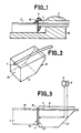
- an end piece or connection block 2 is shown having a groove in which a fiber 1 is placed.
- connection block has a first face 20 which, according to the example of FIG. 2, is substantially perpendicular to the fiber and a second face 21 making an angle (generally 45 °) with the first face 20.
- connection block is placed against a face 30 of an integrated optical circuit 3 with the face 20 parallel to the face 30.
- connection block is then bonded directly to the face 30 of the integrated optical circuit using a layer of adhesive 4.
- connection block could have 3 to 5 mm in length depending on the direction of the fiber 1 and approximately 1 to 2 mm in section side.
- a light source 5 emits a light beam F0 which is transmitted by the face 21 to the double interface between the faces 20 of the connection block and 30 of the integrated optical circuit.
- the light beam F1 received by these interfaces is reflected variably if the two faces 20 and 30 are not parallel. Part of this beam is reflected by the face 20 of the connection block 2 and the other part of the beam is reflected by the face 30 of the integrated optical circuit.
- a beam F2 is reflected and transmits an image representing the interference fringes of the two parts of the beam reflected by the faces 20 and 30, and thus reflecting, on the one hand, the differences in parallelism between the faces 20 and 30, and d 'other share, the distance which separates them, in particular the fringes being black when the faces are in contact.
- the beam F2 is returned by the face 21, in the form of a beam F3 to a device 8 for observing the interference fringes.
- This device 8 can simply be a binocular microscope.
- the faces 20 are bonded. and 30 by introducing the adhesive between the faces 20 and 30 by capillary action. The two faces are then held in parallel, until the adhesive dries.
- connection blocks (2, 2 ⁇ ) are used as described above.
- Each fiber 1, 1 ⁇ , as shown in Figure 8 is placed in a groove made in a faces 22, 22 ⁇ of a block 2, 2 ⁇ . The two faces are then placed opposite.
- the two blocks containing the fibers 1 and 1 ⁇ are pressed against each other by their faces 22 and 22 ⁇ in order to polish the faces 20 and 20 ⁇ .
- connection blocks are connected to the integrated optical circuit by adjusting the parallelism and then bonding the faces 20 and 30 on the one hand and 20 ⁇ and 30 ⁇ on the other hand as described above.
- each connection block 2, 2 ⁇ is manipulated by a clamp 60, 70.
- Each clamp (60, 70) is integral with a first cradle joint (61, 71) which can rotate according to the arrows T1, T ⁇ 1 around an axis perpendicular to the plane of the figure.
- Each cradle is fixed to a wedge-shaped wedge (62, 72), which wedge is secured to a second cradle joint (63, 73) which can rotate according to the arrows T2, T ⁇ 2 around an axis contained in the plane of the figure.
- the wedge-shaped wedges 62 and 72 have their smallest section directed towards each other which allows a movement very close to the clamps 60 and 70 while spreading the joints 63 and 73 as well as the control devices not represented who command them.
- the relative refractive indices of the materials constituting the fiber and the integrated optical circuit have not been considered. Indeed, to take account of these refractive indices, provision should be made for the direction of each fiber to be inclined relative to the direction of propagation of the corresponding integrated optical circuit (31, 31 ⁇ ) as shown in FIG. 6 .
- inclinations relative to the junction faces 30 and 20 must be provided.
- the face 30 of the integrated optical circuit must be polished so that the direction of the guide 31 makes an angle of approximately 10 degrees with the normal to the plane of the face 30.
- the face 20 of the block connection must be polished so that the axis of the fiber 1 makes an angle of approximately 15 degrees with the normal to the plane of the face 20.
- the fiber 1 thus makes an angle of 5 degrees relative to the direction of the guide optics 31 so that the connection is adapted to the differences in indices between the fiber and the integrated optical circuit. It is obvious that in the case of connection of several fibers, each fiber must be connected to an integrated optical circuit while meeting these angular conditions.
- the lighting system of the double interface constituted by the faces 20 and 30 and the observation of the interference fringes returned by this double interface poses a problem.
- the normal to face 20 is not contained in a plane normal to face 21.
- the source 5 emits a beam F1 which is reflected towards the face 21 by the double interface (20-30).
- the face 21 reflects a beam, not shown, in a direction perpendicular to the plane of the figure.
- the face 21 serves to reflect the beam F2 in order to direct it at the output towards the observation device 8.
- the light source and the observation device 8 can be swapped and the directions of the light beams can be reversed. It is obvious that the above description has been given only by way of nonlimiting example and that other variants can be envisaged without departing from the scope of the invention.
Landscapes
- Physics & Mathematics (AREA)
- General Physics & Mathematics (AREA)
- Optics & Photonics (AREA)
- Optical Couplings Of Light Guides (AREA)
Applications Claiming Priority (2)
| Application Number | Priority Date | Filing Date | Title |
|---|---|---|---|
| FR8617889 | 1986-12-19 | ||
| FR8617889A FR2608785B1 (fr) | 1986-12-19 | 1986-12-19 | Dispositif de connexion de fibres optiques a un circuit optique integre et procede de realisation |
Publications (2)
| Publication Number | Publication Date |
|---|---|
| EP0276599A1 true EP0276599A1 (de) | 1988-08-03 |
| EP0276599B1 EP0276599B1 (de) | 1992-09-09 |
Family
ID=9342122
Family Applications (1)
| Application Number | Title | Priority Date | Filing Date |
|---|---|---|---|
| EP87402860A Expired - Lifetime EP0276599B1 (de) | 1986-12-19 | 1987-12-15 | Vorrichtung für die Verbindung von Fasern mit einem integrierten optischen Schaltkreis und deren Herstellungsmethode |
Country Status (6)
| Country | Link |
|---|---|
| US (1) | US4836645A (de) |
| EP (1) | EP0276599B1 (de) |
| JP (1) | JPH07117613B2 (de) |
| KR (1) | KR960013799B1 (de) |
| DE (1) | DE3781669T2 (de) |
| FR (1) | FR2608785B1 (de) |
Cited By (3)
| Publication number | Priority date | Publication date | Assignee | Title |
|---|---|---|---|---|
| DE3831905A1 (de) * | 1988-09-20 | 1990-03-22 | Standard Elektrik Lorenz Ag | Optisches wellenleitermodul mit faserankopplung |
| DE4012747A1 (de) * | 1990-04-21 | 1991-10-24 | Bodenseewerk Geraetetech | Verfahren zur herstellung von feinoptischen stirnflaechen an wellenleitern |
| AU627076B2 (en) * | 1990-03-13 | 1992-08-13 | Sumitomo Electric Industries, Ltd. | Optical module and process of producing the same |
Families Citing this family (20)
| Publication number | Priority date | Publication date | Assignee | Title |
|---|---|---|---|---|
| US5073002A (en) * | 1990-11-30 | 1991-12-17 | Hockaday Bruce D | Self aligning pigtail |
| FR2674033B1 (fr) * | 1991-03-14 | 1993-07-23 | Corning Inc | Composant optique integre a liaison entre un guide d'onde integre et une fibre optique, fonctionnant dans un large domaine de temperature. |
| EP0527604A3 (en) * | 1991-08-07 | 1993-06-16 | Litton Systems, Inc. | Method of coupling an end of optical fibre to a waveguide formed on a substrate |
| US5249245A (en) * | 1992-08-31 | 1993-09-28 | Motorola, Inc. | Optoelectroinc mount including flexible substrate and method for making same |
| EP0652451B1 (de) * | 1993-11-08 | 2001-08-08 | Corning Incorporated | Kopplung von planaren optischen Wellenleitern und optischen Fasern mit geringer Rückreflexion |
| US5926594A (en) * | 1994-08-31 | 1999-07-20 | Litton Systems, Inc. | System and method for aligning and attaching optical fibers to optical waveguides, and products obtained thereby |
| US6487341B1 (en) * | 2000-10-13 | 2002-11-26 | Agere Systems Guardian Corp | Multi-material structure with reduced polarization dependent loss and method therefor |
| US6839474B2 (en) * | 2000-11-16 | 2005-01-04 | Shipley Company, L.L.C. | Optical assembly for coupling with integrated optical devices and method for making |
| US6867377B2 (en) * | 2000-12-26 | 2005-03-15 | Emcore Corporation | Apparatus and method of using flexible printed circuit board in optical transceiver device |
| US6799902B2 (en) | 2000-12-26 | 2004-10-05 | Emcore Corporation | Optoelectronic mounting structure |
| US7021836B2 (en) * | 2000-12-26 | 2006-04-04 | Emcore Corporation | Attenuator and conditioner |
| US6863444B2 (en) | 2000-12-26 | 2005-03-08 | Emcore Corporation | Housing and mounting structure |
| US6905260B2 (en) | 2000-12-26 | 2005-06-14 | Emcore Corporation | Method and apparatus for coupling optical elements to optoelectronic devices for manufacturing optical transceiver modules |
| US6614965B2 (en) | 2001-05-11 | 2003-09-02 | Lightcross, Inc. | Efficient coupling of optical fiber to optical component |
| US6885795B1 (en) | 2002-05-31 | 2005-04-26 | Kotusa, Inc. | Waveguide tap monitor |
| US6947622B2 (en) * | 2002-06-27 | 2005-09-20 | Kotura, Inc. | Wafer level testing of optical components |
| US7308166B1 (en) | 2002-10-08 | 2007-12-11 | Kotura, Inc. | Coupling a light sensor array with an optical component |
| US6863453B2 (en) * | 2003-01-28 | 2005-03-08 | Emcore Corporation | Method and apparatus for parallel optical transceiver module assembly |
| US7805037B1 (en) | 2003-08-19 | 2010-09-28 | Kotura, Inc. | Multiplexer having improved efficiency |
| US7284914B2 (en) * | 2004-06-12 | 2007-10-23 | Avanex Corporation | Structures for small form factor LiNbO3 optical modulator |
Citations (3)
| Publication number | Priority date | Publication date | Assignee | Title |
|---|---|---|---|---|
| FR2497362A1 (fr) * | 1980-12-29 | 1982-07-02 | Thomson Csf | Procede d'alignement d'une fibre optique monomode et d'un guide d'onde integre |
| DE3232508A1 (de) * | 1982-09-01 | 1984-03-01 | Siemens AG, 1000 Berlin und 8000 München | Anordnung zur ermittlung der intensitaet der lichtausstrahlung einer lichtemittierenden diode |
| EP0170457A1 (de) * | 1984-07-13 | 1986-02-05 | BRITISH TELECOMMUNICATIONS public limited company | Verbindung von Wellenleitern |
Family Cites Families (11)
| Publication number | Priority date | Publication date | Assignee | Title |
|---|---|---|---|---|
| US3791715A (en) * | 1972-12-11 | 1974-02-12 | Ibm | System for coupling light from a fiber optic waveguide into a thin film waveguide |
| US3967877A (en) * | 1974-07-16 | 1976-07-06 | International Business Machines (Ibm) | Coupler for coupling optical energy transmitted by optical fiber to optical waveguide and method of manufacture |
| US4130343A (en) * | 1977-02-22 | 1978-12-19 | Bell Telephone Laboratories, Incorporated | Coupling arrangements between a light-emitting diode and an optical fiber waveguide and between an optical fiber waveguide and a semiconductor optical detector |
| JPS54100751A (en) * | 1978-01-24 | 1979-08-08 | Mitsubishi Electric Corp | Detection of connection of optical fibers |
| JPS5924816A (ja) * | 1982-07-31 | 1984-02-08 | Matsushita Electric Works Ltd | 光導波路の接続方法 |
| DE3236149A1 (de) * | 1982-09-29 | 1984-03-29 | Siemens AG, 1000 Berlin und 8000 München | Verfahren zur herstellung von lichtwellenleiter-abzweigern und -multi-/demultiplexern nach dem strahlteilerprinzip |
| JPS6049306A (ja) * | 1983-08-29 | 1985-03-18 | Canon Inc | 導波路光学系 |
| GB2146788B (en) * | 1983-09-20 | 1986-09-24 | Stc Plc | Prism coupling to flat waveguides |
| US4730883A (en) * | 1983-11-28 | 1988-03-15 | Kei Mori | Photoradiator including light control device |
| JPS60172001A (ja) * | 1984-02-17 | 1985-09-05 | Sumitomo Electric Ind Ltd | 光導波路の光フアイバとの結合構造 |
| JPS60191210A (ja) * | 1984-03-13 | 1985-09-28 | Fujitsu Ltd | 光導波路デバイス |
-
1986
- 1986-12-19 FR FR8617889A patent/FR2608785B1/fr not_active Expired
-
1987
- 1987-12-15 EP EP87402860A patent/EP0276599B1/de not_active Expired - Lifetime
- 1987-12-15 DE DE8787402860T patent/DE3781669T2/de not_active Expired - Fee Related
- 1987-12-17 JP JP62317646A patent/JPH07117613B2/ja not_active Expired - Fee Related
- 1987-12-18 KR KR1019870014455A patent/KR960013799B1/ko not_active Expired - Fee Related
- 1987-12-18 US US07/135,083 patent/US4836645A/en not_active Expired - Lifetime
Patent Citations (3)
| Publication number | Priority date | Publication date | Assignee | Title |
|---|---|---|---|---|
| FR2497362A1 (fr) * | 1980-12-29 | 1982-07-02 | Thomson Csf | Procede d'alignement d'une fibre optique monomode et d'un guide d'onde integre |
| DE3232508A1 (de) * | 1982-09-01 | 1984-03-01 | Siemens AG, 1000 Berlin und 8000 München | Anordnung zur ermittlung der intensitaet der lichtausstrahlung einer lichtemittierenden diode |
| EP0170457A1 (de) * | 1984-07-13 | 1986-02-05 | BRITISH TELECOMMUNICATIONS public limited company | Verbindung von Wellenleitern |
Non-Patent Citations (4)
| Title |
|---|
| APPLIED OPTICS, vol. 21, no. 7, 1 avril 1982, pages 1310-1319, Optical Society of America, New York, US; J.T. CHILWELL: "Prism coupler jig. interference fringes enable observation of the coupling gap" * |
| IBM TECHNICAL DISCLOSURE BULLETIN, vol. 25, no. 8, janvier 1983, pages 4095-4096, New York, US; G.A. SHEKITA: "Fiber-optic connector with inherent wrap capability" * |
| PATENT ABSTRACTS OF JAPAN, vol. 10, no. 45 (P-430)[2102], 21 février 1986; & JP-A-60 191 210 (FUJITSU K.K.) 28-09-1985 * |
| PATENT ABSTRACTS OF JAPAN, vol. 3, no. 124 (E-144), 17 octobre 1979, page 81 E 144; & JP-A-54 100 751 (MITSUBISHI DENKI K.K.) 08-08-1979 * |
Cited By (6)
| Publication number | Priority date | Publication date | Assignee | Title |
|---|---|---|---|---|
| DE3831905A1 (de) * | 1988-09-20 | 1990-03-22 | Standard Elektrik Lorenz Ag | Optisches wellenleitermodul mit faserankopplung |
| US4953936A (en) * | 1988-09-20 | 1990-09-04 | Standard Elektrik Lorenz Aktiengesellschaft | Optical waveguide module with fiber coupling |
| EP0360176A3 (en) * | 1988-09-20 | 1990-12-19 | Standard Elektrik Lorenz Aktiengesellschaft | Optical wave guide module with a fibre coupling |
| AU627076B2 (en) * | 1990-03-13 | 1992-08-13 | Sumitomo Electric Industries, Ltd. | Optical module and process of producing the same |
| DE4012747A1 (de) * | 1990-04-21 | 1991-10-24 | Bodenseewerk Geraetetech | Verfahren zur herstellung von feinoptischen stirnflaechen an wellenleitern |
| US5177859A (en) * | 1990-04-21 | 1993-01-12 | Bodenseewerk Geratetechnik Gmbh | Method for manufacturing high-precision end faces on waveguides |
Also Published As
| Publication number | Publication date |
|---|---|
| KR880008042A (ko) | 1988-08-30 |
| KR960013799B1 (ko) | 1996-10-10 |
| JPH07117613B2 (ja) | 1995-12-18 |
| FR2608785B1 (fr) | 1989-08-04 |
| EP0276599B1 (de) | 1992-09-09 |
| DE3781669T2 (de) | 1993-02-04 |
| US4836645A (en) | 1989-06-06 |
| DE3781669D1 (de) | 1992-10-15 |
| FR2608785A1 (fr) | 1988-06-24 |
| JPS63165808A (ja) | 1988-07-09 |
Similar Documents
| Publication | Publication Date | Title |
|---|---|---|
| EP0276599B1 (de) | Vorrichtung für die Verbindung von Fasern mit einem integrierten optischen Schaltkreis und deren Herstellungsmethode | |
| EP0138698B1 (de) | Optischer Wellenlängen-Multiplexer-Demultiplexer für bidirektionale Verbindung | |
| EP3404457A1 (de) | Photonen-chip mit reflektierender struktur zur rückfaltung des lichtwegs | |
| EP0050059A1 (de) | Hybrid-optisches Verbindungselement und Anwendung in einem Ring-Interferometer | |
| EP0646772B1 (de) | Optischer Wellenleiter mit schräger Endfläche | |
| EP2177938A1 (de) | Ausrichtungsstruktur und -verfahren einer optischen Faser auf einem optischen Wellenleiter | |
| EP0346232B1 (de) | Verfahren und System zur Verbindung von Glasfasern ohne Fresnel-Reflexion, veränderlicher optischer Abschwächer und System unter Verwendung desselben zur Messung des Einflusses des Reflexionsgrads auf eine optische Uebertragungsstrecke | |
| EP0674197A1 (de) | Verbindungsvorrichtung für eine Mehrkernfaser und Verfahren zu ihrer Herstellung | |
| FR2560470A1 (fr) | Multiplexeur-demultiplexeur optique de longueurs d'onde utilisant des fibres optiques | |
| EP0863417A1 (de) | Integrierte Multiplex-Verzweigvorrichtung für Mehrkernfasern | |
| US7302119B1 (en) | Polymer phase modulator | |
| EP0018873B1 (de) | Kompakte optische Koppelungsvorrichtung und solch eine Vorrichtung enthaltender interferometrischer Gyrometer mit einer optischen Faser | |
| FR2563627A1 (fr) | Procede et appareil pour l'eclairage en retour de connecteurs optiques | |
| EP0064919B1 (de) | Vorrichtung zur Ein- und/oder Ausgabe eines optischen Signals | |
| EP0429337A1 (de) | Optischer Kopf integrierbar in einem hybriden Schaltkreis | |
| FR2542457A1 (fr) | Piece de reception a fibre optique pour dispositif de couplage et procede de realisation d'un tel dispositif | |
| CA2063208C (fr) | Procede de raccordement de deux cables a fibres optiques par epissurage | |
| FR2548793A1 (fr) | Coupleur optique pour relier des fibres optiques | |
| FR2738921A1 (fr) | Coupleur optique capable d'empecher la sortie d'une lumiere parasite a une extremite d'incidence d'un isolateur optique | |
| EP4168838A1 (de) | Photonischer chip, verfahren zur montage eines optischen teils und des photonischen chips und daraus resultierendes photonisches bauelement | |
| US7239765B1 (en) | Polymer phase modulator | |
| EP0416989B1 (de) | Kopplungsvorrichtung zwischen optischen Übertragungselementen | |
| JPH1068916A (ja) | 光導波路デバイスおよびその製造方法 | |
| JPS6295504A (ja) | 光導波回路 | |
| EP0190962A1 (de) | Vorrichtung für faseroptische Kupplung und Verfahren zu deren Herstellung |
Legal Events
| Date | Code | Title | Description |
|---|---|---|---|
| PUAI | Public reference made under article 153(3) epc to a published international application that has entered the european phase |
Free format text: ORIGINAL CODE: 0009012 |
|
| AK | Designated contracting states |
Kind code of ref document: A1 Designated state(s): DE GB IT NL SE |
|
| 17P | Request for examination filed |
Effective date: 19890119 |
|
| RAP3 | Party data changed (applicant data changed or rights of an application transferred) |
Owner name: THOMSON-CSF |
|
| 17Q | First examination report despatched |
Effective date: 19910613 |
|
| GRAA | (expected) grant |
Free format text: ORIGINAL CODE: 0009210 |
|
| AK | Designated contracting states |
Kind code of ref document: B1 Designated state(s): DE GB IT NL SE |
|
| ITF | It: translation for a ep patent filed | ||
| REF | Corresponds to: |
Ref document number: 3781669 Country of ref document: DE Date of ref document: 19921015 |
|
| GBT | Gb: translation of ep patent filed (gb section 77(6)(a)/1977) | ||
| PLBE | No opposition filed within time limit |
Free format text: ORIGINAL CODE: 0009261 |
|
| STAA | Information on the status of an ep patent application or granted ep patent |
Free format text: STATUS: NO OPPOSITION FILED WITHIN TIME LIMIT |
|
| 26N | No opposition filed | ||
| EAL | Se: european patent in force in sweden |
Ref document number: 87402860.8 |
|
| REG | Reference to a national code |
Ref country code: GB Ref legal event code: IF02 |
|
| PGFP | Annual fee paid to national office [announced via postgrant information from national office to epo] |
Ref country code: SE Payment date: 20050602 Year of fee payment: 18 Ref country code: GB Payment date: 20050602 Year of fee payment: 18 |
|
| PGFP | Annual fee paid to national office [announced via postgrant information from national office to epo] |
Ref country code: NL Payment date: 20050621 Year of fee payment: 18 |
|
| PGFP | Annual fee paid to national office [announced via postgrant information from national office to epo] |
Ref country code: DE Payment date: 20050630 Year of fee payment: 18 |
|
| PG25 | Lapsed in a contracting state [announced via postgrant information from national office to epo] |
Ref country code: IT Free format text: LAPSE BECAUSE OF NON-PAYMENT OF DUE FEES;WARNING: LAPSES OF ITALIAN PATENTS WITH EFFECTIVE DATE BEFORE 2007 MAY HAVE OCCURRED AT ANY TIME BEFORE 2007. THE CORRECT EFFECTIVE DATE MAY BE DIFFERENT FROM THE ONE RECORDED. Effective date: 20051215 Ref country code: GB Free format text: LAPSE BECAUSE OF NON-PAYMENT OF DUE FEES Effective date: 20051215 |
|
| PG25 | Lapsed in a contracting state [announced via postgrant information from national office to epo] |
Ref country code: SE Free format text: LAPSE BECAUSE OF NON-PAYMENT OF DUE FEES Effective date: 20051216 |
|
| PG25 | Lapsed in a contracting state [announced via postgrant information from national office to epo] |
Ref country code: NL Free format text: LAPSE BECAUSE OF NON-PAYMENT OF DUE FEES Effective date: 20060701 Ref country code: DE Free format text: LAPSE BECAUSE OF NON-PAYMENT OF DUE FEES Effective date: 20060701 |
|
| EUG | Se: european patent has lapsed | ||
| GBPC | Gb: european patent ceased through non-payment of renewal fee |
Effective date: 20051215 |
|
| NLV4 | Nl: lapsed or anulled due to non-payment of the annual fee |
Effective date: 20060701 |