EP0279224A1 - Procédé de photopolymérisation de matériaux durcisables sur l'influence de rayonnement UV - Google Patents
Procédé de photopolymérisation de matériaux durcisables sur l'influence de rayonnement UV Download PDFInfo
- Publication number
- EP0279224A1 EP0279224A1 EP88101041A EP88101041A EP0279224A1 EP 0279224 A1 EP0279224 A1 EP 0279224A1 EP 88101041 A EP88101041 A EP 88101041A EP 88101041 A EP88101041 A EP 88101041A EP 0279224 A1 EP0279224 A1 EP 0279224A1
- Authority
- EP
- European Patent Office
- Prior art keywords
- curing
- irradiation
- light
- curing material
- gap
- Prior art date
- Legal status (The legal status is an assumption and is not a legal conclusion. Google has not performed a legal analysis and makes no representation as to the accuracy of the status listed.)
- Granted
Links
- 239000000463 material Substances 0.000 title claims abstract description 46
- 238000000034 method Methods 0.000 title claims abstract description 17
- 239000000853 adhesive Substances 0.000 claims abstract description 12
- 230000001070 adhesive effect Effects 0.000 claims abstract description 12
- 238000006073 displacement reaction Methods 0.000 claims abstract description 4
- 238000003848 UV Light-Curing Methods 0.000 claims description 31
- 239000004922 lacquer Substances 0.000 claims description 8
- 238000001723 curing Methods 0.000 claims description 7
- 230000005855 radiation Effects 0.000 claims description 4
- 239000002966 varnish Substances 0.000 abstract description 3
- 239000011344 liquid material Substances 0.000 description 4
- 238000006552 photochemical reaction Methods 0.000 description 3
- 238000006243 chemical reaction Methods 0.000 description 2
- 239000007788 liquid Substances 0.000 description 2
- 239000000126 substance Substances 0.000 description 2
- 238000005336 cracking Methods 0.000 description 1
- 239000012530 fluid Substances 0.000 description 1
- 238000004519 manufacturing process Methods 0.000 description 1
- 230000003287 optical effect Effects 0.000 description 1
- 230000002250 progressing effect Effects 0.000 description 1
- 230000000750 progressive effect Effects 0.000 description 1
- 230000000007 visual effect Effects 0.000 description 1
Images
Classifications
-
- G—PHYSICS
- G02—OPTICS
- G02B—OPTICAL ELEMENTS, SYSTEMS OR APPARATUS
- G02B6/00—Light guides; Structural details of arrangements comprising light guides and other optical elements, e.g. couplings
- G02B6/24—Coupling light guides
- G02B6/36—Mechanical coupling means
- G02B6/38—Mechanical coupling means having fibre to fibre mating means
-
- G—PHYSICS
- G02—OPTICS
- G02B—OPTICAL ELEMENTS, SYSTEMS OR APPARATUS
- G02B5/00—Optical elements other than lenses
Definitions
- the invention relates to a method for curing UV-curing materials, in particular adhesives and lacquers, by irradiation with UV light.
- UV-curing adhesives and varnishes are used in the manufacture of optical components and in printed circuit board technology, especially conductive adhesives and conductive varnishes. These materials cure very quickly under intensive and even exposure to UV light, e.g. in less than 60 seconds, but always have a volume shrinkage that is within the limits of approx. 2.5 vol.% up to 10 vol.%. On the one hand, good adhesive strength is to be produced, but shrinking of the adhesive or lacquer layer, combined with cracking or blistering, with misplacement or warping or even with breakage of the component, is undesirable and should be avoided. This requires a high level of processing care.
- any cracks that degrade the visual appearance of the parts or reduce the conductivity can be repaired by adding new substance.
- a method of completely avoiding the loss of volume and the corresponding tensions is not yet known.
- the invention has for its object to eliminate the aforementioned disadvantages.
- the irradiation of the UV-curing material is controlled by an aperture such that - The irradiation with UV light begins at at least one point and the irradiated area is concentrically enlarged from this point to the outside or - The irradiation with UV light begins on at least one line and the entire surface of the UV-curing material is irradiated by a relative displacement between the material and the screen in at least one direction.
- the method is consequently designed such that, starting from at least one predetermined point or at least one predetermined line, corresponding to the reaction center or the reaction line, the photochemical reaction continues by moving a front of UV light in the direction of this front.
- the material shrinking during curing can draw liquid material from its not yet hardened environment or from a reservoir.
- a movable front of UV light is created by a variable or movable screen, the material of which is impermeable to UV light.
- a preferred embodiment of this invention is provided by using a perforated diaphragm with a variable diameter.
- the method envisages starting with a small aperture, whereby only a punctiform radiation is generated on the UV-curing material, and then opening the pinhole at a defined speed until the entire surface of the UV-curing material is irradiated by UV light .
- the second-mentioned procedure in claim 1 corresponds to the same inventive idea as the first. It assumes that the photochemical reaction begins on a line, the front of the UV light progressing here by displacing a gap or a partial cover relative to the surface of the UV-curing material.
- An extremely advantageous embodiment of the invention is realized through the use of a movable gap which is moved relative to the UV-curing material.
- the method carried out in this way ensures that a certain point or line of the UV-curing material is exposed by passing over the front limit of the gap in the direction of movement, remains exposed for a time and the exposure is ended after crossing the limit of the gap in the direction of movement.
- a partial cover can also be used as the gap, which at the beginning of the exposure releases only a narrow strip of the UV-curing material for exposure and is subsequently pulled down sideways until the entire surface of the UV-curing material is exposed.
- the defined progression of a front of UV light has an opposite flow of the still fluid subs dance and thus leads to a compensation for the otherwise occurring volume loss.
- the shrinkage in volume can either be completely compensated for or, if it is only of a minor extent, be taken into account from the start, so that the desired layer thicknesses can be set without errors.
- Another particularly advantageous embodiment of the invention provides that the mutual displacement between the movable gap and the UV-curing material takes place at a constant speed. This means that all areas of the UV-curing material have the same exposure time and therefore harden particularly evenly.
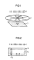
- a surface with UV-curing material 3 is to be exposed by UV light 1, controlled by a pinhole 2, for example an iris.
- the initially small opening of the aperture 21 leads to a correspondingly small point or circular exposure of the UV-curing material, so that a reaction center arises.
- the arrows indicated within the aperture 2 indicate that the aperture is slowly opened during the process until the entire surface of the UV-curing material 3 is sufficiently exposed. With this procedure, no uniform exposure time is achieved for the various locations of the UV-curing material.
- the essential thing, namely to avoid the loss of volume of the material is the concentric progressive circular front of the UV light on the UV-curing material causes. This defined movement of the front of the UV light creates an opposite flow of still liquid substance, which in this case is directed radially inwards towards the reaction center and thus compensates for the volume shrinkage that occurs during curing.
- FIG. 2 shows an area of UV-curing material 5 that is to be exposed by UV light 1.
- the aperture 4 is designed as a gap 41.
- the exposure of the UV-curing material begins on a predetermined side on a line and ensures a constant speed uniform exposure time of all points of the UV-curing material.
- a simple implementation of this version of the method is provided by a fixed UV light source, an underlying aperture in the form of a stationary gap and an underlying conveyor belt on which the components with the UV-curing layers are transported at a constant speed.
- the gap opening width or intensity of the UV light 1 can be set as a function of the material properties of the UV-curing adhesive or lacquer.
Landscapes
- Physics & Mathematics (AREA)
- General Physics & Mathematics (AREA)
- Optics & Photonics (AREA)
- Application Of Or Painting With Fluid Materials (AREA)
- Macromonomer-Based Addition Polymer (AREA)
- Organic Low-Molecular-Weight Compounds And Preparation Thereof (AREA)
Priority Applications (1)
| Application Number | Priority Date | Filing Date | Title |
|---|---|---|---|
| AT88101041T ATE55140T1 (de) | 1987-02-12 | 1988-01-25 | Verfahren zum aushaerten von uv-haertenden materialien. |
Applications Claiming Priority (2)
| Application Number | Priority Date | Filing Date | Title |
|---|---|---|---|
| DE3704416 | 1987-02-12 | ||
| DE3704416 | 1987-02-12 |
Publications (2)
| Publication Number | Publication Date |
|---|---|
| EP0279224A1 true EP0279224A1 (fr) | 1988-08-24 |
| EP0279224B1 EP0279224B1 (fr) | 1990-08-01 |
Family
ID=6320853
Family Applications (1)
| Application Number | Title | Priority Date | Filing Date |
|---|---|---|---|
| EP88101041A Expired - Lifetime EP0279224B1 (fr) | 1987-02-12 | 1988-01-25 | Procédé de photopolymérisation de matériaux durcisables sur l'influence de rayonnement UV |
Country Status (3)
| Country | Link |
|---|---|
| EP (1) | EP0279224B1 (fr) |
| AT (1) | ATE55140T1 (fr) |
| DE (1) | DE3860371D1 (fr) |
Citations (6)
| Publication number | Priority date | Publication date | Assignee | Title |
|---|---|---|---|---|
| CH555747A (fr) * | 1972-07-12 | 1974-11-15 | Blattner & Picard | Masque, pour tracer des lignes de largeur constante par impression d'une couche photosensible notamment pour la fabrication de negatifs de circuits imprimes. |
| DE2620173A1 (de) * | 1976-05-07 | 1977-11-10 | Storz Karl | Strahlungsblende |
| EP0114345A2 (fr) * | 1982-12-27 | 1984-08-01 | Western Electric Company, Incorporated | Composite de multifilaments durcissable par irradiation |
| DE3339754A1 (de) * | 1983-01-31 | 1984-08-02 | Jenoptik Jena Gmbh, Ddr 6900 Jena | Verfahren zur herstellung von klebstoffen |
| EP0197423A1 (fr) * | 1985-03-27 | 1986-10-15 | Mitsubishi Rayon Co., Ltd. | Méthode de photopolymérisation continue de monomères vinyliques solubles dans l'eau |
| EP0206545A1 (fr) * | 1985-05-31 | 1986-12-30 | Corning Glass Works | Procédé et dispositif pour revêtir à nouveau des fibres optiques |
-
1988
- 1988-01-25 EP EP88101041A patent/EP0279224B1/fr not_active Expired - Lifetime
- 1988-01-25 AT AT88101041T patent/ATE55140T1/de not_active IP Right Cessation
- 1988-01-25 DE DE8888101041T patent/DE3860371D1/de not_active Expired - Lifetime
Patent Citations (6)
| Publication number | Priority date | Publication date | Assignee | Title |
|---|---|---|---|---|
| CH555747A (fr) * | 1972-07-12 | 1974-11-15 | Blattner & Picard | Masque, pour tracer des lignes de largeur constante par impression d'une couche photosensible notamment pour la fabrication de negatifs de circuits imprimes. |
| DE2620173A1 (de) * | 1976-05-07 | 1977-11-10 | Storz Karl | Strahlungsblende |
| EP0114345A2 (fr) * | 1982-12-27 | 1984-08-01 | Western Electric Company, Incorporated | Composite de multifilaments durcissable par irradiation |
| DE3339754A1 (de) * | 1983-01-31 | 1984-08-02 | Jenoptik Jena Gmbh, Ddr 6900 Jena | Verfahren zur herstellung von klebstoffen |
| EP0197423A1 (fr) * | 1985-03-27 | 1986-10-15 | Mitsubishi Rayon Co., Ltd. | Méthode de photopolymérisation continue de monomères vinyliques solubles dans l'eau |
| EP0206545A1 (fr) * | 1985-05-31 | 1986-12-30 | Corning Glass Works | Procédé et dispositif pour revêtir à nouveau des fibres optiques |
Non-Patent Citations (1)
| Title |
|---|
| PATENT ABSTRACTS OF JAPAN, Band 8, Nr. 163 (P-290)[1600], 27. Juli 1984; & JP-A-59 058 401 (TOUSHIBA DENZAI K.K.) 04-04-1984 * |
Also Published As
| Publication number | Publication date |
|---|---|
| ATE55140T1 (de) | 1990-08-15 |
| EP0279224B1 (fr) | 1990-08-01 |
| DE3860371D1 (de) | 1990-09-06 |
Similar Documents
| Publication | Publication Date | Title |
|---|---|---|
| DE3825366C2 (de) | Photopolymerisationsverfahren zur kontinuierlichen Herstellung eines Acrylpolymergels und Vorrichtung dazu | |
| DE4125534A1 (de) | Verfahren und vorrichtung zum herstellen eines objekts mittels stereograhpie | |
| DE3112631A1 (de) | Gewindeteile fuer selbstsichernde schraubverbindungen und verfahren zu deren herstellung | |
| WO2001045860A2 (fr) | Procede et dispositif de revetement de surface d'un element de construction interne de vehicules automobiles | |
| EP0239158A2 (fr) | Plaque de circuit pour circuits imprimés et procédé de fabrication d'une telle plaque | |
| DE2316192C2 (de) | Lagervorrichtung aus Kunststoff | |
| EP3689581A1 (fr) | Dispositif de fabrication additive | |
| WO1994006608A1 (fr) | Procede et dispositif pour enlever mecaniquement une couche situee sur le materiau de base d'un support d'informations se presentant sous forme de disque | |
| DE29606258U1 (de) | Gegenstand mit mattierter Oberfläche | |
| DE102007017842B4 (de) | Vorrichtung zum Aktivieren einer polymerisierbaren Masse | |
| DE68902168T2 (de) | Vorrichtung und verfahren zum herstellen einer rotationssiebdruckschablone. | |
| DE4401455B4 (de) | Flüssigkristall-Anzeige | |
| DE102008057784A1 (de) | Verfahren und Vorrichtung zum Herstellen von Volumen-Transmissions-und/oder -Reflexionshologrammen | |
| EP0279224B1 (fr) | Procédé de photopolymérisation de matériaux durcisables sur l'influence de rayonnement UV | |
| DE602004006426T2 (de) | Nicht auslaufendes klebstoffsystem und seine verwendung im immersionsobjektiv | |
| EP0701487A1 (fr) | Dispositif de laquage ou d'enduction de plaques ou de panneaux | |
| EP1185412B1 (fr) | Dispositif permettant la jonction de substrats | |
| DE1442472A1 (de) | Verfahren und Vorrichtung zur Entfernung von Verunreingungen aus Fluessigkeiten mit hohem elektrischem Widerstand | |
| DE4214259C1 (en) | Gradient optic mfg. - rotates crucible with molten glass or plastics to disperse heavier mols evenly and radially outwards for refractive index change | |
| EP0929367A1 (fr) | Procede et dispositif de traitement de substrats | |
| WO1995005901A1 (fr) | Dispositif pour le vernissage de substrats dans la fabrication de semi-conducteurs | |
| DE3331596A1 (de) | Vorrichtung und verfahren zum aufbringen eines ueberzugs auf eine zylindrische platte | |
| DE3505468A1 (de) | Verfahren und vorrichtung zum entschichten von lackbeschichtungen | |
| DE2932724C2 (de) | Gerät zum Entlacken von lichtwellenleitern | |
| DE20019557U1 (de) | Vorrichtung zum Zusammenkleben erster und zweiter Plattenelemente bei der Herstellung einer DVD |
Legal Events
| Date | Code | Title | Description |
|---|---|---|---|
| PUAI | Public reference made under article 153(3) epc to a published international application that has entered the european phase |
Free format text: ORIGINAL CODE: 0009012 |
|
| AK | Designated contracting states |
Kind code of ref document: A1 Designated state(s): AT BE CH DE FR GB IT LI NL SE |
|
| 17P | Request for examination filed |
Effective date: 19881010 |
|
| 17Q | First examination report despatched |
Effective date: 19891102 |
|
| GRAA | (expected) grant |
Free format text: ORIGINAL CODE: 0009210 |
|
| AK | Designated contracting states |
Kind code of ref document: B1 Designated state(s): AT BE CH DE FR GB IT LI NL SE |
|
| REF | Corresponds to: |
Ref document number: 55140 Country of ref document: AT Date of ref document: 19900815 Kind code of ref document: T |
|
| REF | Corresponds to: |
Ref document number: 3860371 Country of ref document: DE Date of ref document: 19900906 |
|
| ET | Fr: translation filed | ||
| ITF | It: translation for a ep patent filed | ||
| GBT | Gb: translation of ep patent filed (gb section 77(6)(a)/1977) | ||
| PGFP | Annual fee paid to national office [announced via postgrant information from national office to epo] |
Ref country code: AT Payment date: 19901219 Year of fee payment: 4 |
|
| PGFP | Annual fee paid to national office [announced via postgrant information from national office to epo] |
Ref country code: FR Payment date: 19910121 Year of fee payment: 4 |
|
| PGFP | Annual fee paid to national office [announced via postgrant information from national office to epo] |
Ref country code: BE Payment date: 19910124 Year of fee payment: 4 |
|
| PGFP | Annual fee paid to national office [announced via postgrant information from national office to epo] |
Ref country code: SE Payment date: 19910125 Year of fee payment: 4 |
|
| PG25 | Lapsed in a contracting state [announced via postgrant information from national office to epo] |
Ref country code: LI Free format text: LAPSE BECAUSE OF NON-PAYMENT OF DUE FEES Effective date: 19910131 Ref country code: CH Free format text: LAPSE BECAUSE OF NON-PAYMENT OF DUE FEES Effective date: 19910131 |
|
| PGFP | Annual fee paid to national office [announced via postgrant information from national office to epo] |
Ref country code: NL Payment date: 19910131 Year of fee payment: 4 |
|
| PLBI | Opposition filed |
Free format text: ORIGINAL CODE: 0009260 |
|
| 26 | Opposition filed |
Opponent name: ROEHM GMBH Effective date: 19910429 |
|
| NLR1 | Nl: opposition has been filed with the epo |
Opponent name: ROEHM GMBH. |
|
| REG | Reference to a national code |
Ref country code: CH Ref legal event code: PL |
|
| PG25 | Lapsed in a contracting state [announced via postgrant information from national office to epo] |
Ref country code: DE Effective date: 19911001 |
|
| ITTA | It: last paid annual fee | ||
| PG25 | Lapsed in a contracting state [announced via postgrant information from national office to epo] |
Ref country code: BE Effective date: 19920131 |
|
| RDAG | Patent revoked |
Free format text: ORIGINAL CODE: 0009271 |
|
| STAA | Information on the status of an ep patent application or granted ep patent |
Free format text: STATUS: PATENT REVOKED |
|
| 27W | Patent revoked |
Effective date: 19920208 |
|
| GBPR | Gb: patent revoked under art. 102 of the ep convention designating the uk as contracting state | ||
| BERE | Be: lapsed |
Owner name: SIEMENS A.G. Effective date: 19920131 |
|
| NLR2 | Nl: decision of opposition | ||
| EUG | Se: european patent has lapsed |
Ref document number: 88101041.7 Effective date: 19920624 |