EP0280198A1 - Verfahren zur Herstellung einer Diamantschicht - Google Patents
Verfahren zur Herstellung einer Diamantschicht Download PDFInfo
- Publication number
- EP0280198A1 EP0280198A1 EP88102388A EP88102388A EP0280198A1 EP 0280198 A1 EP0280198 A1 EP 0280198A1 EP 88102388 A EP88102388 A EP 88102388A EP 88102388 A EP88102388 A EP 88102388A EP 0280198 A1 EP0280198 A1 EP 0280198A1
- Authority
- EP
- European Patent Office
- Prior art keywords
- gas
- ion beam
- series
- beam irradiation
- carbon
- Prior art date
- Legal status (The legal status is an assumption and is not a legal conclusion. Google has not performed a legal analysis and makes no representation as to the accuracy of the status listed.)
- Granted
Links
- 229910003460 diamond Inorganic materials 0.000 title claims abstract description 57
- 239000010432 diamond Substances 0.000 title claims abstract description 57
- 238000000034 method Methods 0.000 title claims abstract description 26
- 238000010884 ion-beam technique Methods 0.000 claims abstract description 86
- 239000000758 substrate Substances 0.000 claims abstract description 51
- OKTJSMMVPCPJKN-UHFFFAOYSA-N Carbon Chemical compound [C] OKTJSMMVPCPJKN-UHFFFAOYSA-N 0.000 claims abstract description 45
- 229910052799 carbon Inorganic materials 0.000 claims abstract description 41
- 239000010409 thin film Substances 0.000 claims abstract description 29
- 230000008021 deposition Effects 0.000 claims abstract description 10
- 239000007789 gas Substances 0.000 claims description 89
- 239000010408 film Substances 0.000 claims description 31
- 238000001704 evaporation Methods 0.000 claims description 20
- 230000008020 evaporation Effects 0.000 claims description 18
- 239000011261 inert gas Substances 0.000 claims description 18
- 239000004215 Carbon black (E152) Substances 0.000 claims description 17
- 229930195733 hydrocarbon Natural products 0.000 claims description 17
- 150000002430 hydrocarbons Chemical class 0.000 claims description 17
- 150000002894 organic compounds Chemical class 0.000 claims description 16
- UFHFLCQGNIYNRP-UHFFFAOYSA-N Hydrogen Chemical compound [H][H] UFHFLCQGNIYNRP-UHFFFAOYSA-N 0.000 claims description 15
- 230000001678 irradiating effect Effects 0.000 claims 11
- 235000010627 Phaseolus vulgaris Nutrition 0.000 claims 1
- 244000046052 Phaseolus vulgaris Species 0.000 claims 1
- 150000002500 ions Chemical class 0.000 description 25
- OKTJSMMVPCPJKN-IGMARMGPSA-N Carbon-12 Chemical compound [12C] OKTJSMMVPCPJKN-IGMARMGPSA-N 0.000 description 17
- 238000000151 deposition Methods 0.000 description 7
- 150000003376 silicon Chemical class 0.000 description 7
- 230000015572 biosynthetic process Effects 0.000 description 6
- 229910002804 graphite Inorganic materials 0.000 description 5
- 239000010439 graphite Substances 0.000 description 5
- 239000000463 material Substances 0.000 description 5
- VNWKTOKETHGBQD-UHFFFAOYSA-N methane Chemical compound C VNWKTOKETHGBQD-UHFFFAOYSA-N 0.000 description 4
- -1 silicon ions Chemical class 0.000 description 4
- 238000007796 conventional method Methods 0.000 description 3
- 239000013078 crystal Substances 0.000 description 3
- 229910052734 helium Inorganic materials 0.000 description 3
- 239000012535 impurity Substances 0.000 description 3
- 239000000203 mixture Substances 0.000 description 3
- 239000002245 particle Substances 0.000 description 3
- CSCPPACGZOOCGX-UHFFFAOYSA-N Acetone Chemical compound CC(C)=O CSCPPACGZOOCGX-UHFFFAOYSA-N 0.000 description 2
- XKRFYHLGVUSROY-UHFFFAOYSA-N Argon Chemical compound [Ar] XKRFYHLGVUSROY-UHFFFAOYSA-N 0.000 description 2
- OTMSDBZUPAUEDD-UHFFFAOYSA-N Ethane Chemical compound CC OTMSDBZUPAUEDD-UHFFFAOYSA-N 0.000 description 2
- 229910052786 argon Inorganic materials 0.000 description 2
- 238000001816 cooling Methods 0.000 description 2
- 230000007547 defect Effects 0.000 description 2
- 238000005566 electron beam evaporation Methods 0.000 description 2
- 230000005284 excitation Effects 0.000 description 2
- 238000010438 heat treatment Methods 0.000 description 2
- 229910052754 neon Inorganic materials 0.000 description 2
- 239000008188 pellet Substances 0.000 description 2
- 229910052710 silicon Inorganic materials 0.000 description 2
- 239000010703 silicon Substances 0.000 description 2
- BLRPTPMANUNPDV-UHFFFAOYSA-N Silane Chemical compound [SiH4] BLRPTPMANUNPDV-UHFFFAOYSA-N 0.000 description 1
- XUIMIQQOPSSXEZ-UHFFFAOYSA-N Silicon Chemical compound [Si] XUIMIQQOPSSXEZ-UHFFFAOYSA-N 0.000 description 1
- 150000001721 carbon Chemical class 0.000 description 1
- 238000005229 chemical vapour deposition Methods 0.000 description 1
- PZPGRFITIJYNEJ-UHFFFAOYSA-N disilane Chemical compound [SiH3][SiH3] PZPGRFITIJYNEJ-UHFFFAOYSA-N 0.000 description 1
- 230000000694 effects Effects 0.000 description 1
- 238000010891 electric arc Methods 0.000 description 1
- 238000010894 electron beam technology Methods 0.000 description 1
- 239000001307 helium Substances 0.000 description 1
- SWQJXJOGLNCZEY-UHFFFAOYSA-N helium atom Chemical compound [He] SWQJXJOGLNCZEY-UHFFFAOYSA-N 0.000 description 1
- 239000001257 hydrogen Substances 0.000 description 1
- 229910052739 hydrogen Inorganic materials 0.000 description 1
- 229910052743 krypton Inorganic materials 0.000 description 1
- 238000004949 mass spectrometry Methods 0.000 description 1
- 238000005268 plasma chemical vapour deposition Methods 0.000 description 1
- 229910052704 radon Inorganic materials 0.000 description 1
- 238000004544 sputter deposition Methods 0.000 description 1
- 239000000126 substance Substances 0.000 description 1
- 230000002194 synthesizing effect Effects 0.000 description 1
- 238000007738 vacuum evaporation Methods 0.000 description 1
- 239000012808 vapor phase Substances 0.000 description 1
- 238000000927 vapour-phase epitaxy Methods 0.000 description 1
- 229910052724 xenon Inorganic materials 0.000 description 1
Images
Classifications
-
- C—CHEMISTRY; METALLURGY
- C23—COATING METALLIC MATERIAL; COATING MATERIAL WITH METALLIC MATERIAL; CHEMICAL SURFACE TREATMENT; DIFFUSION TREATMENT OF METALLIC MATERIAL; COATING BY VACUUM EVAPORATION, BY SPUTTERING, BY ION IMPLANTATION OR BY CHEMICAL VAPOUR DEPOSITION, IN GENERAL; INHIBITING CORROSION OF METALLIC MATERIAL OR INCRUSTATION IN GENERAL
- C23C—COATING METALLIC MATERIAL; COATING MATERIAL WITH METALLIC MATERIAL; SURFACE TREATMENT OF METALLIC MATERIAL BY DIFFUSION INTO THE SURFACE, BY CHEMICAL CONVERSION OR SUBSTITUTION; COATING BY VACUUM EVAPORATION, BY SPUTTERING, BY ION IMPLANTATION OR BY CHEMICAL VAPOUR DEPOSITION, IN GENERAL
- C23C14/00—Coating by vacuum evaporation, by sputtering or by ion implantation of the coating forming material
- C23C14/22—Coating by vacuum evaporation, by sputtering or by ion implantation of the coating forming material characterised by the process of coating
- C23C14/221—Ion beam deposition
-
- C—CHEMISTRY; METALLURGY
- C23—COATING METALLIC MATERIAL; COATING MATERIAL WITH METALLIC MATERIAL; CHEMICAL SURFACE TREATMENT; DIFFUSION TREATMENT OF METALLIC MATERIAL; COATING BY VACUUM EVAPORATION, BY SPUTTERING, BY ION IMPLANTATION OR BY CHEMICAL VAPOUR DEPOSITION, IN GENERAL; INHIBITING CORROSION OF METALLIC MATERIAL OR INCRUSTATION IN GENERAL
- C23C—COATING METALLIC MATERIAL; COATING MATERIAL WITH METALLIC MATERIAL; SURFACE TREATMENT OF METALLIC MATERIAL BY DIFFUSION INTO THE SURFACE, BY CHEMICAL CONVERSION OR SUBSTITUTION; COATING BY VACUUM EVAPORATION, BY SPUTTERING, BY ION IMPLANTATION OR BY CHEMICAL VAPOUR DEPOSITION, IN GENERAL
- C23C14/00—Coating by vacuum evaporation, by sputtering or by ion implantation of the coating forming material
- C23C14/06—Coating by vacuum evaporation, by sputtering or by ion implantation of the coating forming material characterised by the coating material
- C23C14/0605—Carbon
- C23C14/0611—Diamond
-
- C—CHEMISTRY; METALLURGY
- C30—CRYSTAL GROWTH
- C30B—SINGLE-CRYSTAL GROWTH; UNIDIRECTIONAL SOLIDIFICATION OF EUTECTIC MATERIAL OR UNIDIRECTIONAL DEMIXING OF EUTECTOID MATERIAL; REFINING BY ZONE-MELTING OF MATERIAL; PRODUCTION OF A HOMOGENEOUS POLYCRYSTALLINE MATERIAL WITH DEFINED STRUCTURE; SINGLE CRYSTALS OR HOMOGENEOUS POLYCRYSTALLINE MATERIAL WITH DEFINED STRUCTURE; AFTER-TREATMENT OF SINGLE CRYSTALS OR A HOMOGENEOUS POLYCRYSTALLINE MATERIAL WITH DEFINED STRUCTURE; APPARATUS THEREFOR
- C30B23/00—Single-crystal growth by condensing evaporated or sublimed materials
- C30B23/02—Epitaxial-layer growth
-
- C—CHEMISTRY; METALLURGY
- C30—CRYSTAL GROWTH
- C30B—SINGLE-CRYSTAL GROWTH; UNIDIRECTIONAL SOLIDIFICATION OF EUTECTIC MATERIAL OR UNIDIRECTIONAL DEMIXING OF EUTECTOID MATERIAL; REFINING BY ZONE-MELTING OF MATERIAL; PRODUCTION OF A HOMOGENEOUS POLYCRYSTALLINE MATERIAL WITH DEFINED STRUCTURE; SINGLE CRYSTALS OR HOMOGENEOUS POLYCRYSTALLINE MATERIAL WITH DEFINED STRUCTURE; AFTER-TREATMENT OF SINGLE CRYSTALS OR A HOMOGENEOUS POLYCRYSTALLINE MATERIAL WITH DEFINED STRUCTURE; APPARATUS THEREFOR
- C30B29/00—Single crystals or homogeneous polycrystalline material with defined structure characterised by the material or by their shape
- C30B29/02—Elements
- C30B29/04—Diamond
Definitions
- the present invention relates to a method of forming a diamond film on a substrate through vacuum evaporation and ion beam irradiation and apparatus therefor.
- a chemical vapor-phase epitaxy method such as a plasma CVD method, a photo CVD method, or the like, using a gas of hydrocarbon series or an organic compound has been employed as means for forming or synthesizing a diamond film on a substrate.
- evaporation of carbon and ion beam irradiation are performed on a substrate in a vacuum so as to form a diamond thin film on the substrate.
- an ion beam obtained by ionizing an inert gas is used for the ion beam irradiation.
- an ion beam obtained by ionizing a gas of at least one kind selected from gases including a gas of hydrocarbon series, a gas of organic compound series, a gas of silicon series, and a hydrogen gas, or a mixture of the above-mentioned gas of at least one kind and an inert gas may be used for the ion beam irradiation.
- a carbon ion beam may be used.
- the diamond film forming apparatus of the present invention comprises a plate for holding a substrate, a carbon evaporation source, and ion beam irradiation means.
- the irradiation ions act as a nucleus formation energy supply source for causing carbon of graphite structure deposited on the substrate to grow into crystals of diamond, thereby forming a diamond thin film on the substrate.
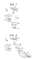
- Fig. 1 is a schematic view showing a first embodiment of the apparatus for carrying out the method according to the present invention.
- a substrate for example, a base plate
- a holder 2 is housed in a vacuum vessel (not shown), and an evaporation source 8 and an ion source 16 are provided in opposition to the substrate 4.
- the evaporation source 8 shown in Fig. 1 is an electron beam evaporation source which has a carbon pellet as an evaporation material 10 so that carbon 12 obtained by heat-evaporation of the carbon pellet 10 by means of an electron beam can be deposited on a surface of the substrate 4.
- carbon since carbon has sublimating property, there is a case where the film forming velocity by means of such an electron beam evaporation source is too slow to attain the purpose for forming diamond film.
- an evaporation source of the type in which a target including carbon is sputtered by inert gas ion irradiation or by magnetron discharge an evaporation source of the type in which carbon is evaporated by vacuum arc discharge at a cathode made of carbon, or the like, or any combination of the foregoing evaporation sources may be as the evaporation source 8.
- the ion source 16 may be, for example, an ion source of the bucket type using a cusped magnet field for plasma confinement.
- a uniformly-ionized ion beam 18 having large sectional area can be irradiated onto the surface of the substrate 4, so that a large area of the substrate 4 can be treated at a time.
- a monitor 14 is provided to observe the thickness of a thin film to be formed on the substrate 4.
- the ion beam 18 may be an inert gas ion beam, specifically, a beam of ions of one kind or more selected from He, Ne, Ar, Kr, Xe, and Rn.
- a single or mixed gas selected from the inert gases as described above is used as the gas G to be fed to the ion source 16.
- a single or mixed gas of at least one kind selected from a gas of hydrocarbon series (such as a methane gas, an ethane gas, or the like), a gas of an organic compound series (such as acetone, or the like), a gas of silicon series (such as a monosilane gas, a disilane gas, or the like), and a hydrogen gas can also be used as the gas G to be fed to the ion source 16.
- the gas may be mixed or diluted with an inert gas (such as an argon gas, a helium gas, or the like) to be used as the gas G.
- gas G the gas of hydrocarbon series, the gas of organic compound series, the gas of silicon series, and the hydrogen gas are preferable as the gas G:
- the carbon 12 from the evaporation source 8 is deposited onto the substrate 4. Simultaneously or alternately with the deposition, the ion beam 18 from the ion source 16 is made to irradiate the substrate 4.
- the ratio (composition ratio) of the number of particles of the irradiation ions to that of the deposited carbon 12, that is ion/carbon is selected to a value within a range of from about 0.1% to 100%, and, specifically, is selected to be a suitable value in the above range in accordance with the energy of the ion beam 18 and the velocity of evaporation of the carbon 12.
- the ratio of the number of particles of the silicon ions irradiated in the form of the ion beam 18 to that of the carbon 12 deposited on the substrate 4 is sufficient if it is selected to a value within a range of from about 0.1% to about 10%.
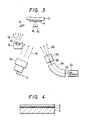
- the ion irradiation acts as a nucleus forming energy supply source for making the carbon 12 having the graphite structure and deposited on the substrate 4 grow into diamond crystals to thereby form a diamond thin film 6 on the surface of the substrate 4, as shown in Fig. 4.
- the energy of the ion beam 18 is a low value not higher than about 10 KeV, more preferably not higher than about several hundreds electron volts. While there is no particular lower limit, the energy should not be lower than about 10 eV in practical use because there is a limit in drawing the ion beam 18 out of the ion source 16.
- the irradiation angle ⁇ 1 (that is, the angle between the direction of the ion beam 18 and a normal onto the surface of the substrate 4 as shown in Fig. 1) is selected to be a value within a range of from 0° to about 60°, so that sputtering of the deposited carbon 12 due to the irradiation of the ion beam 18 can be suppressed to a small amount.
- the substrate 4 may be heated by heating means (not shown) to about several hundreds degree (°C) or may be cooled by cooling means (not shown). If the substrate 4 is heated, not only the reaction for diamond formation can be hastened by thermal excitation but also defect portions caused in the diamond thin film 6 can be removed in the process of forming the film. If cooled, the substrate 4 can be protected when the substrate 4 is weak against heat.
- Fig. 2 shows a second embodiment of the apparatus according to the present invention.
- a carbon ion beam is used as the ion beam in place of those used in the first embodiment.
- a substrate for example, a base plate
- a vacuum vessel (not shown)
- an evaporation source 8 is provided in opposition to the substrate 4, similarly to the first embodiment.
- a beam line constituted by an ion source 20, a mass spectrograph 24, and a scanning electrode 28 is provided in place of the ion source 16 in the first embodiment.
- the evaporation source 8 is the same as that in the first embodiment, and may be of any one of various evaporation types or systems.
- the ion source 20 is arranged as follows:
- An ion beam 22 including carbon ions is drawn out from the ion source 20 with predetermined energy.
- the ion beam 22 is subject to mass spectrometry by means of the mass spectrograph 24 or the like so as to extract a carbon ion beam 26.
- the carbon ion beam 26 is scanned by the scanning electrode 28 or the like in the X- and Y-direction as shown in Fig. 2, in which Y-direction directs normally to the surface of the drawing.
- the carbon ion beam 26 is enlarged in its sectional area, and the enlarged beam 26 is irradiated onto the surface of the substrate 4.
- the method of film formation in the second embodiment is quite the same as that in the first embodiment. That is, in forming a film, after the inside of the vacuum vessel has been exhausted, for example, to about 10 ⁇ 5 to 10 ⁇ 7 Torr, the carbon 12 from the evaporation source 8 is deposited onto the substrate 4. Simultaneously or alternately with the deposition, the ion beam 26 from the ion source 16 is made to irradiate the substrate 4. Furthermore, for the same reason as that in the case of the ion beam 18, preferably, the energy of the carbon ion beam 26 is selected to be a value within a range of from about 10 eV to about 10 KeV, and more preferably in a range of from about 10 eV to about several hundreds eV.
- the irradiation angle ⁇ 2 of the carbon ion beam 26 relative to the substrate 4 is selected to be a value within a range of from 0° to about 60°.
- the particle ratio (composition ratio) of the irradiation carbon ions 26 relative to the deposited carbon 12, that is, the rate of ion/carbon is selected to be a value within a range of from about 0.1% to 100%, and specifically, a suitable value is selected within the range in accordance with the energy of the carbon ion beam 26 and the velocity of deposition of the carbon.
- heating means or cooling means may be provided as in the first embodiment.
- Fig. 3 is a schematic view showing a third embodiment of the apparatus for carrying out the method according to the present invention.
- the apparatus of the third embodiment is a combination of the apparatuses of the first and second embodiments. That is, a gas ion beam 18 and a carbon ion beam 26 are irradiated onto carbon 12 deposited on a substrate 4.
- the gas ion beam 18 may be an ion beam of an inert gas or an ion beam of a gas of at least one kind selected from an inert gas, a gas of hydrocarbon series, a gas of organic compound series, a gas of silicon series, and a hydrogen gas, or an ion beam of a mixed gas of an inert gas and a gas of at least one kind selected from a gas of hydrocarbon series, a gas of organic compound series, a gas of silicon series, and a hydrogen gas.
- the irradiation carbon ions 26 act not only as a nucleus forming energy supply source as described already but also as a film forming carbon supply source, so that there is a further feature that the velocity of formation of the diamond thin film 6 is further improved in addition to the features (1) to (6) listed already.
- the present invention not only the deposition of graphite can be suppressed but also a high-quality diamond thin film containing no impurity therein can be efficiently formed. Furthermore, since low temperature treatment can be attained, the range of selection of the materials which can be used as the substrate is extremely widened. Furthermore, the adhesion of the diamond thin film onto the substrate can be improved.
Landscapes
- Chemical & Material Sciences (AREA)
- Engineering & Computer Science (AREA)
- Materials Engineering (AREA)
- Metallurgy (AREA)
- Organic Chemistry (AREA)
- Crystallography & Structural Chemistry (AREA)
- Chemical Kinetics & Catalysis (AREA)
- Mechanical Engineering (AREA)
- Crystals, And After-Treatments Of Crystals (AREA)
- Physical Vapour Deposition (AREA)
Applications Claiming Priority (6)
| Application Number | Priority Date | Filing Date | Title |
|---|---|---|---|
| JP37576/87 | 1987-02-19 | ||
| JP37579/87 | 1987-02-19 | ||
| JP37578/87 | 1987-02-19 | ||
| JP3757887A JPS63206388A (ja) | 1987-02-19 | 1987-02-19 | ダイヤモンド薄膜の作製方法 |
| JP3757687A JPS63206387A (ja) | 1987-02-19 | 1987-02-19 | ダイヤモンド薄膜の作製方法 |
| JP3757987A JPS63206389A (ja) | 1987-02-19 | 1987-02-19 | ダイヤモンド薄膜の作製方法 |
Publications (2)
| Publication Number | Publication Date |
|---|---|
| EP0280198A1 true EP0280198A1 (de) | 1988-08-31 |
| EP0280198B1 EP0280198B1 (de) | 1992-09-02 |
Family
ID=27289513
Family Applications (1)
| Application Number | Title | Priority Date | Filing Date |
|---|---|---|---|
| EP88102388A Expired - Lifetime EP0280198B1 (de) | 1987-02-19 | 1988-02-18 | Verfahren zur Herstellung einer Diamantschicht |
Country Status (2)
| Country | Link |
|---|---|
| EP (1) | EP0280198B1 (de) |
| DE (1) | DE3874165T2 (de) |
Cited By (4)
| Publication number | Priority date | Publication date | Assignee | Title |
|---|---|---|---|---|
| EP0609621A1 (de) * | 1992-12-16 | 1994-08-10 | General Electric Company | Verfahren zum Ermitteln der Dicke von CVD-Schichten |
| US6315871B1 (en) * | 1999-11-30 | 2001-11-13 | The United States Of America As Represented By The United States Department Of Energy | Method for forming diamonds from carbonaceous material |
| WO2001036704A3 (en) * | 1999-11-19 | 2001-12-20 | Epion Corp | Method and apparatus for forming carbonaceous film |
| CN113228225A (zh) * | 2019-01-18 | 2021-08-06 | 应用材料股份有限公司 | 低发射覆层以及离子植入器 |
Citations (1)
| Publication number | Priority date | Publication date | Assignee | Title |
|---|---|---|---|---|
| US4490229A (en) * | 1984-07-09 | 1984-12-25 | The United States Of America As Represented By The Administrator Of The National Aeronautics And Space Administration | Deposition of diamondlike carbon films |
-
1988
- 1988-02-18 EP EP88102388A patent/EP0280198B1/de not_active Expired - Lifetime
- 1988-02-18 DE DE8888102388T patent/DE3874165T2/de not_active Expired - Lifetime
Patent Citations (1)
| Publication number | Priority date | Publication date | Assignee | Title |
|---|---|---|---|---|
| US4490229A (en) * | 1984-07-09 | 1984-12-25 | The United States Of America As Represented By The Administrator Of The National Aeronautics And Space Administration | Deposition of diamondlike carbon films |
Non-Patent Citations (2)
| Title |
|---|
| PATENT ABSTRACTS OF JAPAN, vol. 10, no. 49 (C-330)[2106], 26th February 1986; & JP-A-60 195 094 (KOGYO GIJUTSUIN) 03-10-1985 * |
| THIN SOLID FILMS, vol. 96, no. 1, October 1982, pages 31-44, Elsevier Sequoia, Lausanne, CH; C. WEISSMANTEL et al.: "Preparation and properties of hard i-C and i-BN coatings" * |
Cited By (6)
| Publication number | Priority date | Publication date | Assignee | Title |
|---|---|---|---|---|
| EP0609621A1 (de) * | 1992-12-16 | 1994-08-10 | General Electric Company | Verfahren zum Ermitteln der Dicke von CVD-Schichten |
| WO2001036704A3 (en) * | 1999-11-19 | 2001-12-20 | Epion Corp | Method and apparatus for forming carbonaceous film |
| US6416820B1 (en) | 1999-11-19 | 2002-07-09 | Epion Corporation | Method for forming carbonaceous hard film |
| US6315871B1 (en) * | 1999-11-30 | 2001-11-13 | The United States Of America As Represented By The United States Department Of Energy | Method for forming diamonds from carbonaceous material |
| CN113228225A (zh) * | 2019-01-18 | 2021-08-06 | 应用材料股份有限公司 | 低发射覆层以及离子植入器 |
| CN113228225B (zh) * | 2019-01-18 | 2024-04-23 | 应用材料股份有限公司 | 离子植入器、处理离子束的方法以及低发射嵌件 |
Also Published As
| Publication number | Publication date |
|---|---|
| DE3874165T2 (de) | 1992-12-17 |
| EP0280198B1 (de) | 1992-09-02 |
| DE3874165D1 (de) | 1992-10-08 |
Similar Documents
| Publication | Publication Date | Title |
|---|---|---|
| EP0245688B1 (de) | Verfahren zur Herstellung einer Diamantenschicht | |
| EP0266178B1 (de) | Verfahren und Anordnung zur Herstellung einer dünnen Schicht | |
| EP0280315B1 (de) | Verfahren zur Herstellung eines Diamantfilms | |
| US4657774A (en) | Method for thin film formation | |
| US4800100A (en) | Combined ion and molecular beam apparatus and method for depositing materials | |
| US4656052A (en) | Process for production of high-hardness boron nitride film | |
| EP0288608B1 (de) | Anlage zur Bildung einer Dünnschicht | |
| JPH0381294B2 (de) | ||
| EP0399470B1 (de) | Verfahren zur Erzeugung einer Dünnschicht mittels Strahlablagerung | |
| EP0280198B1 (de) | Verfahren zur Herstellung einer Diamantschicht | |
| Chin et al. | Preparation of Si3N4 coatings by ion plating | |
| JP2603919B2 (ja) | 立方晶系窒化ホウ素の結晶粒を含む窒化ホウ素膜の作製方法 | |
| JPH0663087B2 (ja) | 窒化チタン膜の形成方法 | |
| JPH086171B2 (ja) | 炭素系膜の形成方法 | |
| JPH031377B2 (de) | ||
| JPH0610338B2 (ja) | ホウ素薄膜の形成方法 | |
| JPH0582467B2 (de) | ||
| JP3389639B2 (ja) | 膜の内部応力制御方法 | |
| JP2769404B2 (ja) | 炭素−窒素化合物膜の形成方法 | |
| JPS63206388A (ja) | ダイヤモンド薄膜の作製方法 | |
| JPH0524999A (ja) | 炭化珪素薄膜の製造方法 | |
| JPH0795510B2 (ja) | X線露光用マスクの製造方法 | |
| JPS63262457A (ja) | 窒化ホウ素膜の作製方法 | |
| JP3174313B2 (ja) | 薄膜形成装置 | |
| JP2004327905A (ja) | 薄膜材料の形成方法および形成装置 |
Legal Events
| Date | Code | Title | Description |
|---|---|---|---|
| PUAI | Public reference made under article 153(3) epc to a published international application that has entered the european phase |
Free format text: ORIGINAL CODE: 0009012 |
|
| AK | Designated contracting states |
Kind code of ref document: A1 Designated state(s): DE FR GB |
|
| 17P | Request for examination filed |
Effective date: 19890214 |
|
| 17Q | First examination report despatched |
Effective date: 19890802 |
|
| GRAA | (expected) grant |
Free format text: ORIGINAL CODE: 0009210 |
|
| AK | Designated contracting states |
Kind code of ref document: B1 Designated state(s): DE FR GB |
|
| REF | Corresponds to: |
Ref document number: 3874165 Country of ref document: DE Date of ref document: 19921008 |
|
| ET | Fr: translation filed | ||
| PLBE | No opposition filed within time limit |
Free format text: ORIGINAL CODE: 0009261 |
|
| STAA | Information on the status of an ep patent application or granted ep patent |
Free format text: STATUS: NO OPPOSITION FILED WITHIN TIME LIMIT |
|
| 26N | No opposition filed | ||
| PGFP | Annual fee paid to national office [announced via postgrant information from national office to epo] |
Ref country code: GB Payment date: 19940208 Year of fee payment: 7 |
|
| PGFP | Annual fee paid to national office [announced via postgrant information from national office to epo] |
Ref country code: FR Payment date: 19940225 Year of fee payment: 7 |
|
| PGFP | Annual fee paid to national office [announced via postgrant information from national office to epo] |
Ref country code: DE Payment date: 19940331 Year of fee payment: 7 |
|
| PG25 | Lapsed in a contracting state [announced via postgrant information from national office to epo] |
Ref country code: GB Effective date: 19950218 |
|
| GBPC | Gb: european patent ceased through non-payment of renewal fee |
Effective date: 19950218 |
|
| PG25 | Lapsed in a contracting state [announced via postgrant information from national office to epo] |
Ref country code: FR Effective date: 19951031 |
|
| PG25 | Lapsed in a contracting state [announced via postgrant information from national office to epo] |
Ref country code: DE Effective date: 19951101 |
|
| REG | Reference to a national code |
Ref country code: FR Ref legal event code: ST |