EP0280582B1 - Graphische Computersysteme - Google Patents
Graphische Computersysteme Download PDFInfo
- Publication number
- EP0280582B1 EP0280582B1 EP88301742A EP88301742A EP0280582B1 EP 0280582 B1 EP0280582 B1 EP 0280582B1 EP 88301742 A EP88301742 A EP 88301742A EP 88301742 A EP88301742 A EP 88301742A EP 0280582 B1 EP0280582 B1 EP 0280582B1
- Authority
- EP
- European Patent Office
- Prior art keywords
- viewport
- memory
- display
- priority
- window
- Prior art date
- Legal status (The legal status is an assumption and is not a legal conclusion. Google has not performed a legal analysis and makes no representation as to the accuracy of the status listed.)
- Expired - Lifetime
Links
- 238000013507 mapping Methods 0.000 claims abstract description 20
- 238000012545 processing Methods 0.000 claims abstract description 12
- 238000000034 method Methods 0.000 claims description 9
- 238000012546 transfer Methods 0.000 claims description 6
- 230000008569 process Effects 0.000 claims description 5
- 238000000605 extraction Methods 0.000 claims description 4
- 238000009795 derivation Methods 0.000 claims 1
- 230000004048 modification Effects 0.000 abstract description 4
- 238000012986 modification Methods 0.000 abstract description 4
- 239000000872 buffer Substances 0.000 description 17
- 230000000694 effects Effects 0.000 description 11
- 230000006870 function Effects 0.000 description 5
- 238000013459 approach Methods 0.000 description 4
- 238000010586 diagram Methods 0.000 description 4
- 230000008901 benefit Effects 0.000 description 3
- 230000010076 replication Effects 0.000 description 3
- 230000001360 synchronised effect Effects 0.000 description 3
- 238000012360 testing method Methods 0.000 description 3
- 230000003139 buffering effect Effects 0.000 description 2
- 230000008859 change Effects 0.000 description 2
- 238000005516 engineering process Methods 0.000 description 2
- 238000011068 loading method Methods 0.000 description 2
- 230000000007 visual effect Effects 0.000 description 2
- 238000007792 addition Methods 0.000 description 1
- 230000005540 biological transmission Effects 0.000 description 1
- 230000001010 compromised effect Effects 0.000 description 1
- 238000010276 construction Methods 0.000 description 1
- 238000000354 decomposition reaction Methods 0.000 description 1
- 230000007547 defect Effects 0.000 description 1
- 238000013461 design Methods 0.000 description 1
- 238000002059 diagnostic imaging Methods 0.000 description 1
- 239000000284 extract Substances 0.000 description 1
- 230000009191 jumping Effects 0.000 description 1
- 238000004519 manufacturing process Methods 0.000 description 1
- 230000000873 masking effect Effects 0.000 description 1
- 238000002156 mixing Methods 0.000 description 1
- 238000002360 preparation method Methods 0.000 description 1
- 230000004044 response Effects 0.000 description 1
- 239000007787 solid Substances 0.000 description 1
- 238000003860 storage Methods 0.000 description 1
- 230000007704 transition Effects 0.000 description 1
Images





Classifications
-
- G—PHYSICS
- G09—EDUCATION; CRYPTOGRAPHY; DISPLAY; ADVERTISING; SEALS
- G09G—ARRANGEMENTS OR CIRCUITS FOR CONTROL OF INDICATING DEVICES USING STATIC MEANS TO PRESENT VARIABLE INFORMATION
- G09G5/00—Control arrangements or circuits for visual indicators common to cathode-ray tube indicators and other visual indicators
- G09G5/14—Display of multiple viewports
Definitions
- the present invention generally concerns improvements in or relating to computer graphics systems, and more particularly concerns window management systems and windowing devices for use with computer graphics workstations.
- images to be displayed on a display screen are drawn into a reserved block of memory, sometimes called a frame buffer, within the system.
- Memory locations within the frame buffer have a one-to-one correspondence with display locations on the display screen and image data is read out sequentially from the frame buffer via video generation circuitry in accordance with the instantaneous address of the scanning beam on the display screen.
- This arrangement is adequate so long as there is no requirement to move complex multiple images rapidly around the display screen.
- the requirements of graphics systems users have become more sophisticated there has been a corresponding increase in demand for complex images to be displayable and quickly relocatable on a screen.
- the position and size of a displayed image may be controlled by the user, for example by way of a mouse which provides user determined positional and dimensional information.
- a mouse can be moved swiftly across a table top by the user for repositioning a displayed image
- the image is commonly unable to keep up with the movement of the mouse. This is because of the one-to-one relationship which exists between the frame buffer and the display screen locations and because of the corresponding requirement that, in order to move an image from one part of the screen to another, it is necessary to copy the entire image data to new locations in memory and to replace the image data at the original memory locations by data corresponding to whatever was visually behind the image on the screen, whether it be a plain background or part of another image.
- Hardware windowing is a method of moving images around a display screen without the need to rearrange large blocks of image data within the memory.
- Image data in the frame buffer is transferred to the video generation circuitry in a controlled sequence such that any given area of memory, hereinafter referred to as a window, can be displayed at any chosen location on the display screen, such location hereinafter being referred to as a viewport.
- Hardware windowing is distinct from conventional serialised approaches wherein scanning through the display memory is effected sequentially as the display screen is scanned, since in hardware windowing a dedicated circuit is used to extract image data from the memory by jumping from place to place in memory as required. It then becomes easy to move any image instantly from one place to another, simply by specifying where it is to be displayed next.
- An exemplary hardware windowing system is disclosed in WO-A-8502049.
- the present invention resides in the concept of providing a multi-planar display memory wherein each plane of the memory has its own viewport controller for flexibly mapping windows from that memory plane to viewports of the display.
- a hardware windowing system for use with a computer graphics facility for determining the transfer of image data from any chosen window in memory and the display of the image represented by said data at any chosen viewport location of a display, the hardware windowing system comprising a plurality of viewport controllers each controller being individually coupled to a single plane of a multi-planar memory for individually supervising the transfer of data from one or more windows in its associated memory plane to viewports in the display.
- the present invention overcomes all of the above-mentioned problems of prior art computer graphics systems, and uniquely provides a number of hitherto unachievable benefits to the art of window management.
- the exemplary windowing device in accordance with the present invention which is described hereinafter is configured as a single VLSI component designed for use with planar display memory and to take advantage of the special capabilities of modern VRAM memory chips. It is modular and cascadable and can be used with almost any planar VRAM raster scan graphics system. It provides a means by which multiple windows can be displayed in viewports at high resolution with each viewport and window sized and located with perfect, single-pixel resolution. It handles overlapping viewports automatically and allows them to appear transparent or opaque relative to one another as required.
- a single windowing device as hereinafter described comprises a pluraity of viewport controllers each capable of mapping a plurality of 1-bit windows from a respective plane of a multi-planar memory to viewports on the screen.
- each windowing device comprises four viewport controllers, each of which controls the manipulation of up to four windows on a single image plane.
- a plurality of such windowing devices can be cascaded to address any number of memory planes and enable any number of windows to be displayed in an arrangement which will hereinafter be referred to as a windowing device array.
- This highly modular architecture allows price and performance to be tailored precisely to the user's needs, in systems ranging from PCs to top-end graphics workstations.
- the windowing device treats the display memory as a collection of superimposed bit planes.
- a 1-bit window is any rectangular array of bits on one plane
- an n-bit window is a block of image data composed of n superimposed 1-bit windows of equal size and each drawn from a different plane.
- Each 1-bit window may be taken from any arbitrary location in its memory plane and displayed in any viewport location, and any combination of n planes is allowed.
- the conventional concept of a window corresponds in the system of the present invention to the restricted case of an n-bit window in which all the 1-bit components are at the same planar address (vertically aligned) and n is equal to the number of planes in the system.
- each 1-bit window is assigned a priority by the user, the same priority being assigned to all n planar components of an n-bit window.
- a higher priority window is arranged to obscure a lower priority window. This obscuring is a visual effect only and does not involve the manipulation of the image data in memory, and the obscured area re-appears automatically and instantaneously when the overlapping viewport is moved or when the priorities are suitably altered.
- Equal priority windows from different planes are advantageously arranged to overlap transparently, and colour mixing effects within the overlap area can be determined at the choice of the user by appropriate setting up of a user programmable colour look-up table.
- a viewport of any shape can readily be created by using a 1-bit window as a mask. Double- (or multiple-) buffering of animated images is easily achieved by mapping windows to viewports sequentially; only the areas of the display memory which actually contain the buffered images are affected.
- window-viewport assignments which are a set of absolute and relative co-ordinates on the display and in the memory.
- This simple method of defining windows and viewports makes programming of a graphics system in accordance with the present invention very straightforward, and abolishes the cumbersome software operations such as strip decomposition and Boolean computation of transparency effects which hinder other systems.
- the invention thus provides an extremely versatile, powerful system which enables complex visual effects to be produced effortlessly while making very efficient use of memory. All window boundary clipping and transparency effects are carried out automatically, in real time, with no user intervention.
- the windowing device is effectively invisible to the drawing processor (or whatever other device is being used to create bit maps in memory) and in general drawing proceeds at close to full speed under most circumstances even while the images being drawn are being moved all over the screen.
- the bus bandwidth required to create, relocate or remove a window is so small that the system overhead that this represents is in general negligible.
- windowing device array there is no theoretical limit to the number of windowing devices and therefore viewport controllers that a windowing device array can contain. It follows that there is no theoretical limit to the number of planes, windows and viewports which can be controlled by such an array.
- means can be provided for linking as many of the devices together in parallel as may be required in order to achieve the desired number of displayable viewports.
- a conventional raster graphics system might comprise a host computer 1 which provides overall management of the system, a display memory 2 for storing image data, a raster scan display screen 3 for displaying viewports, and a serialiser 4 which steps in strict progression through the display memory in raster fashion and reads data serially out from the memory as the display spot scans the display screen.
- the resulting display is a one-to-one mapping of the image data onto the display screen so that images appear on the screen in the same relative positions as they are stored in memory.
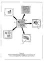
- the hardware windowing system of Figure 1B allows selected areas of memory to be displayed instantly at any desired display position.
- the hardware circuit 5 Under control of the host computer, the hardware circuit 5 performs the function of selectively extracting portions of image data from any location in the display memory 2 and transferring it for display at any desired location on the display screen 3 so that any given area of memory can be displayed at any chosen location on the screen.
- the host computer 1 can be arranged to draw image data directly into the display memory, or it can be used to control a separate drawing processor, not shown, which provides this function.
- the display memory can contain information relating to a number of different images, shown in the Figures exemplarily as a solid chevron 6, a bounded-W 7, and a chequered ball 8.
- the data representative of these images can be stored in different areas of a single memory plane, or can be stored in different memory planes, or with some of the image data in one plane and other image data in one or more other planes.
- the windowing device 5 of the present invention under supervisory control of the host computer 1 which provides to the windowing device 5 window-viewport mapping assignments including information representative of the locations in memory where image data is stored in a window of the memory and the viewport locations whereat such image data is desired to be displayed and representative also of the priority to be accorded to the respective viewports for enabling overlapping viewports to be readily handled, extracts from the display memory 2 only image data appropriate to the required display and passes it to the display screen 3 for display as the information is required.
- the relative locations of the three images 6, 7 and 8 on the display screen 3 need bear no direct correspondence with the relative locations of the corresponding image data in the display memory 2 and can be varied as desired.
- image data of the three images has in the example of Figure 1B been read from the memory and displayed in a manner which causes portions of them to overlap on the display screen, the chevron 6 opaquely overlapping a portion of the chequered ball 8 and the bounded-W 7 and chequered ball 8 transparently sharing a common area of overlap.
- the windowing device 5 of the present invention provides the logic and other functions required to ensure that only the required image data is read from the display memory and transferred to the display screen for display and that, in a case where images overlap transparently, overlapping data from the images is combined before being displayed on the display screen.
- Figure 2 shows further examples of how the present invention enables image data stored in the display memory to be selectively extracted from memory and flexibly displayed on the display screen.
- overlapping viewports are handled by storing image data in multiple memory planes and assigning priorities to window-viewport mapping instructions so that data is automatically read from memory in accordance with the priority assignments and when displayed automatically provides the desired overlapping display effect.
- the display 9 shown in Figure 2 is the same as that described with reference to Figure 1B and shows the features of opaque and transparent overlapping previously mentioned herein, the chevron 6 opaquely overlapping the chequered ball 8 which in turn transparently overlaps the bounded-W 7, such a display being obtainable in accordance with the teachings of the present invention by storing the bounded-W and the chevron in one display memory plane and the ball in another and setting the priority of the chevron at a high value and the priorities of the bounded-W and the ball at the same lower priority.
- equal priority images read from different memory planes overlap transparently in the system of the invention.
- the box 7a is overlapped and partially obscured by the chequered ball 8 and the W 7b overlies and partially obscures both the box 7a and the chequered ball 8, whilst the chevron 6 opaquely overlaps both the box 7a and the ball 8.
- the display 10 of Figure 2 might for example be obtained by storing image data representative of the chevron, the W, the ball and the box in different planes of a multi-planar memory and providing that the box has the lowest priority, the ball has a higher priority than the box but a lower priority than the W, and the chevron has a higher priority than either the box or the ball.
- display effects additional to those obtained by allocation of display images to selected planes of the display memory and by allocation of viewport priorities can be obtained by suitably programming a colour look-up table to which the video signals extracted from memory are applied before they are displayed.
- the windowing device 5 advantageously comprises four viewport controllers which share common areas of control and can each control up to four independent viewports and four associated image windows held in a single memory plane.
- a single windowing device 5 can thus control up to sixteen 1-bit windows held in four 1-bit deep memory planes to produce displays in up to sixteen viewports on a display screen.
- Multi-bit windows consisting of superimposed bits in the four bit planes can likewise be managed.
- the windowing device is adapted to be cascaded to form a windowing device array as aforementioned comprising a plurality of windowing devices arranged in parallel, and such an array can control the display of data from a large number of memory planes independently and can display up to four independent image windows from each plane of memory.
- the invention is not restricted to configuring the windowing device as comprising four viewport controllers, but by virtue of the use of VLSI technology a particularly advantageous chip configuration can be obtained with four viewport controllers on each chip without placing undue demands on the pin count and die size of the VLSI circuitry.
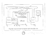
- FIG. 3 there is shown therein a typical graphics system according to the present invention which incorporates a windowing device 5 comprising four independently operable viewport controllers.
- the windowing device 5 is adapted to be controlled by a host computer, not shown, via a host computer bus 11, and there is also provided a drawing processor 12 which draws or creates bit-maps in a planar video RAM 13 which is treated by the windowing device 5 as four superimposed bit planes each of which is individually associated with a specific one of the four viewport controllers within the windowing device.
- the drawing processor may optionally be excluded from the system in which case the host computer may be linked directly to the video RAM 13 so that it can draw directly into the memory.
- the planar video RAM or VRAM, is shown as comprising four independent memory planes 13a-13d, and each memory plane can contain image data drawn into it by the drawing processor 12 and is arranged to be accessed independently by a specific one of the four viewport controllers within the windowing device.
- the viewport controllers operate to extract image data from the VRAM under control of the host computer and to transmit the extracted data to a user programmable colour look-up table and digital to analog converter (CLUT & DAC) 14 which control the display screen 3.
- CLUT & DAC digital to analog converter
- the components shown in Figure 3 are obtainable as standard off-the-shelf components from a wide range of suppliers.
- the drawing processor 12 may be almost any processing device or system capable of creating image data in the form of bit-maps to be stored in the planar VRAM 13.
- a particularly effective planar drawing processor in this respect is the QPDM manufactured by Advanced Micro Devices (UK) Limited.
- the choice of VRAM 13 and of CLUT & DAC 14 is not limited to specific makes or models.
- the embodiment of the invention herein described is optimised for use with the Brooktree range of RAM DAC's which are provided with a suitable programmable colour look-up table and in addition offer multiplexed pixel ports thereby avoiding the need for external multiplexing circuitry.
- Figure 4 shows a functional block diagram of a windowing device 5 according to the invention, the device comprising four viewport controllers 15 only one of which is shown for the sake of clarity, together with functional blocks which are shared by all four viewport controllers within the windowing device, namely a counter 16 for synchronising the windowing device operation with the drawing processor and the raster display, a VRAM controller 17 responsive to the viewport controllers 15 for determining the extraction of image data from the VRAM 13, and global priority control logic 18 for controlling the overlapping display of viewports originating from memory planes controlled by different windowing devices of a windowing device array.
- a counter 16 for synchronising the windowing device operation with the drawing processor and the raster display
- VRAM controller 17 responsive to the viewport controllers 15 for determining the extraction of image data from the VRAM 13
- global priority control logic 18 for controlling the overlapping display of viewports originating from memory planes controlled by different windowing devices of a windowing device array.
- the viewport controller 15 is shown in Figure 4 decomposed into its major subunits, namely a register file 19, a VRAM setup list (VSL) 20, merge logic and video data buffer 21, video control logic 22 and planar priority control logic 23, and the functions and the detailed construction of these subunits will be described in the following, it being remembered at all times that the windowing device of Figure 4 does in fact comprise four such viewport controllers 15.
- VSL VRAM setup list
- each viewport controller In operation of each viewport controller, information identifying the locations in the VRAM display memory of the image windows and the viewport locations where the image windows are required to be displayed together with viewport priority information is downloaded into the register file 19 from the host computer via the host interface 24, it being recalled that each viewport controller 15 can control the display of up to four viewports.
- the information downloaded into the register file 19 is used to create a VRAM setup list which describes the actions to be performed by the VRAM controller 17 in extracting image data from the VRAM for display.
- the data output from the VRAM serial port is input a byte at a time to merge logic and video data buffer 21 which, under the control of information stored in the register file 19, shifts and merges the bytes of data which would each correspond to displays at a plurality of display pixels to achieve the required single pixel display accuracy before passing them to the video controller 22.
- the video controller 22 accepts the merged data and outputs it under control of the priority controller 23 for display.
- Video data is loaded from the VRAM into each of the four viewport controllers eight pixels at a time and is output to the display four pixels at a time, and the video controller takes care of this 8:4 multiplex operation; by virtue of this arrangement the maximum on-chip clock rate required is reduced to one quarter of the pixel rate, making the bandwidth required for high-resolution displays readily achievable using conventional CMOS fabrication.
- the viewport priority information that is loaded into the register file 19 is utilized by the planar priority controller 23 to determine the display in overlapping viewports of image data extracted from that memory plane of the VRAM display memory which is associated with the respective viewport controller.
- the global priority controller 18 co-operates with the four planar priority controllers 23 within the windowing device in order to determine which viewport data originating from the four memory planes controlled by the windowing device should be passed to the display for a given display location.
- the global priority controller 18 also includes a priority bus interface which enables it to communicate over a priority bus 25 with other global priority controllers in similar windowing devices when several such windowing devices are connected in parallel to form a windowing device array as described hereinbefore.
- the global priority controller thus has the capability to determine the display of overlapping viewports corresponding to image data derived from different viewport controllers whether or not these are contained within the same windowing device.
- a handshake interface is provided between the VRAM controller 17 and the drawing processor 12 which requires the transmission between the VRAM controller and the drawing processor of video bus request ( VBR ) and video bus grant ( VBG ) control signals. This interface ensures that the viewport controller and the drawing processor do not both attempt to gain control of the VRAM at the same time.
- Each viewport controller contains three first in first out (FIFO) buffers, namely a VRAM setup list FIFO (VSL FIFO) 26 which together with test logic and VRAM setup list (VSL) compiler 27 and offset adder 28 the functions whereof will be explained hereinafter makes up the VRAM setup list 20 of Figure 4, a data FIFO 29 corresponding to the buffer between the merge logic 21 and the video controller 22, and a priority FIFO 30 which buffers priority information from the register file 19 to the planar priority controller 23.
- the three FIFO's taken together amount to less than 700 bits of buffering per viewport controller which is approximately one quarter of the storage that would be required with a serial line buffer approach.
- the four viewport controllers in the windowing device operate independently and only interact at their output stages where their outputs are synchronised so that identically defined viewports in separate controllers overlap precisely on the display.
- each of the four available window-viewport assignments is defined by data downloaded from the host computer and held in registers within the register file 19.
- the window-viewport co-ordinate definition comprises:
- the viewport X1, Y1 and X2, Y2 co-ordinates define the screen locations of opposite corners of the viewport.
- the offset co-ordinates X o , Y o are added to the viewport X1, Y1 co-ordinates to provide the window start address in memory.
- the viewport priorities are defined by a 3-bit priority word which enables priority levels from 0 to 7 to be achieved, though it will be appreciated that this is exemplary and that greater or lesser numbers of priority levels can be provided for as desired.
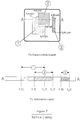
- Figures 7A and 7B show respectively a possible arrangement of three 1-bit deep viewports V1, V2, V3 from a single memory plane where viewport V2 has been assigned a higher priority than viewport V1, and a scanline A-A of the display.
- the viewport controllers operate independently and asynchronously except for their output stages where priority between planes is compared by the global priority controllers.
- the following description applies to the operation of one viewport controller only.
- the process of determining which pixel data is to be displayed in a given scan line begins in the preceding scan line time period, during which the VSL FIFO 26 is loaded with information from VSL compiler 27.
- the VSL compiler 27 thus loads the VRAM setup list into the VSL FIFO 26 in preparation for the following line.
- the VSL compiler 27 calculates the sequence in which viewport data is to be extracted from the VRAM.
- VSL compiler 27 determines the viewport priority hierarchy for the memory plane in question.
- the VSL compiler makes no reference to the priorities of viewports on other planes.
- Information loaded into the VSL FIFO 26 consists of an ordered sequence of entries, each entry being in the form (X e , V#, S, P) where X e is the X address at which the next visible viewport boundary occurs, V# is the number of the active viewport (1-4) at that boundary, S is a setup bit which signals whether or not a VRAM setup is required, that is to say whether the boundary in question is followed by window data (i.e. marks the start of a window) or by background (i.e. marks the end of a window), and P is a parity bit which signals whether VCOUNT is odd or even for the line in question.
- the sequence of entries from the VSL compiler into the VSL FIFO would be as follows: where each X i (n) is the relevant X-co-ordinate obtained from the register file 42.
- the scan line has effectively been divided into a number of data fields.
- the first data field from the leftmost side of the display to X1(1), is formed of background or default data since there is no viewport in this section of display.
- the second data field between X1(1) and X1(2), is formed of viewport V1 pixel data.
- the third data field, from X1(2) to X2(2), can be broken down into two parts. The first part from X1(2) to X2(1) is common to both viewport V1 and viewport V2 but, since viewport V2 has a higher priority than viewport V1, the information associated with this part of the third field is exclusively viewport V2 pixel data.
- the hardware assembles this list of entries from the VSL compiler into the VSL FIFO for the scan line A-A of Figure 7B by working through the X edges defined in the register file 42 in order from left to right across the scan line in a series of logical passes.
- the logic tests each viewport to determine whether Y1(n) ⁇ Y A - A ⁇ Y2(n) indicating that viewport n is relevant to scanline A-A and identifies the relevant viewport which has the smallest value of X1(n), namely the viewport V1.
- a flag-bit is set noting the fact that the left (X1) edge of this viewport has been passed. If the viewport has the highest priority of all viewports active at the boundary location tested, and it is not already the current display viewport, then the four fields of data X e , V#, S and P above are loaded into the VSL FIFO 26.
- the X2 address of the viewport in question will be examined instead of the X1 address during future passes so that the right edge, as seen on the screen, rather than the left edge will next be tested.
- a second flag-bit is set which prevents that viewport from being subject to any testing in subsequent passes. Further similar passes are now made, examining X1 or X2 for each viewport or ignoring the viewport altogether as dictated by the set flag-bits. This continues until all viewports have been logically eliminated. In practice it is possible to accomplish the entire process of detecting viewports for a given scan line well within the time of a single scan line.
- the VSL FIFO buffer 26 is sufficiently large to buffer data for up to two consecutive scan lines, thereby enabling data for the next line to be loaded whilst the data for the current line is being read.
- the parity bit is provided in order to signal the transition to a new line since it toggles on each successive scan line.
- the contents of the VSL FIFO 26 is combined with offset data from the register file 19 and the result is used by the VRAM controller 17 to perform the correct sequence of VRAM setups for the scan line in question.
- this process begins during the flyback period preceding scan line A-A.
- the VRAM controller 17 is a finite state machine and only one such VRAM controller is provided in the windowing device 5. In a windowing device array, all the VRAM controllers run synchronously. During the line flyback time before line A-A, any entry in the VRAM setup list in VSL FIFO 26 will cause the VRAM controller 17 to request control of the VRAM address bus from the drawing processor by asserting the not-VBR (Video Bus Request) signal.
- VBR Video Bus Request
- VBG Video Bus Grant
- the VRAM controller 17 sets up the VRAM serial ports on each memory plane to access data for the first viewport to appear from that memory plane. Once set up, each VRAM serial port is clocked until a number of words equal to the difference between successive values of X e have been output. The next setup operation is then performed.
- the VRAM controller can simultaneously supply four setup addresses (one per memory plane). It determines which planes are set up on a particular cycle by controlling the not-RAS (Row Address Strobe) signal for each plane.
- Image data is extracted from the VRAM in eight bit words and loaded into the merge logic 21.
- the VRAM is organised in 16-bit words and a 16:8 multiplexing operation is performed by alternately output-enabling the VRAM making up the high and low bytes.
- Data bytes output sequentially from the VRAM enter the merge logic 21 which, as is explained more fully below, shifts, masks and merges the data to single pixel resolution as specified by the values of the four bit quantities start-bit, stop-bit and offset-bit. These correspond to the least significant 4-bits of X1(n), X2(n) and X o (n) respectively, and define viewport boundaries and image offsets down to single pixel accuracy.
- FIGS. 8A, 8B and 8C show respectively a schematic block diagram of the merge logic circuit, a graphical depiction of the relationship between byte locations on the display and image bytes as fetched from memory, and a graphical representation of a corresponding sequence of merge logic operations.
- a viewport starts at bit 2 of display byte D1, and the user has decreed that bit 6 of memory byte M1 should appear at this location.
- These bit locations are defined by the bottom three bits of X e and X o . These are 2 and 4 respectively.
- the merge logic must fetch image bytes and generate display bytes, masking off those bits which fall outside of the viewport boundary. Referring to Figure 8A, in this exemplary situation the merge logic operates as follows.
- Memory byte M1 is loaded into input register 31 and is barrel shifted in barrel shifter 32 as defined by the bit offset, which is 4 in the case under consideration. Since the viewport starts in background, register 33 will be clear.
- the appropriate mask is applied to multiplexer 34 to select the low order two bits from register 33 and the high order six bits from the barrel shifter 32.
- the result is stored in register 33 by setting the control bit of multiplexer 35 appropriately, selecting the feedback path.
- register 33 As register 33 is loaded, register 31 receives memory byte M2 which is therefore also shifted.
- the mask applied to multiplexer 34 is now changed to select the most significant four bits from the barrel shifter 32 and the least significant four bits from the register 33. Multiplexer 35 control bit also changes to select the shifter output. This results in the first disply byte D1.
- the whole sequence is shown in Figure 8C for the exemplary situation of Figure 8B.
- the merged data from the merge logic 21 is loaded into data FIFO 29 to achieve the necessary output synchronisation.
- the FIFO 29 is 8-bits wide by 32-bits deep and is equipped with a "FULL" output which halts the data coming in from the VRAM when necessary.
- the presence of the data FIFO 29 allows the viewport controller to start accessing the VRAM during the line flyback time, and buffers sufficient pixel data to enable a steady output of pixels to be passed to the display. It is important that this feature is included since the data stream from the VRAM into the merge logic is fragmented whenever the VRAM controller resets the VRAM serial port between windows.
- the data On exit from the data FIFO, the data enters the video control logic 22 which multiplexes the 8-bit words into 4-bit subwords, controls the synchronisation of the data FIFO 29, and injects zero "background" data during intervals when no viewport is active so that the data FIFO 29 only has to buffer active pixel data.
- viewport edge information X e emerging from the VSL FIFO 26 is selectively loaded into the priority FIFO 30 together with appropriate priority data from the register file 19.
- This loading process is arranged so that priority values corresponding to the 4-bit video subword which contains a given viewport edge are merged into the row of the priority FIFO 30 corresponding to that edge. More particularly, as each VRAM set-up list entry is presented by the VSL FIFO 26, the value X e is compared with the previous value of X e at the top of the priority FIFO 30, and if it falls in a different subword the priority FIFO 30 is loaded.
- each X e entry Associated with each X e entry are four priority entries, one for each of the bits within the subword, which are loaded from the register file 19 at the same time as X e .
- the priority FIFO 30 When two or more successive values of X e fall within a common subword, the priority FIFO 30 is not shifted, but the "overlapped" priority values are updated. The result is a set of four priorities which will correspond precisely to the four display data bits at the video output.
- the output from the priority FIFO 30 is synchronised with the output from the video control logic 22 so that the correct four priority values are presented for each four-bit subword.
- the value of HCOUNT is continuously compared with the X address at the top of the priority FIFO 30.
- the priorities of the bits in a 4-bit subword are output to the planar priority control logic 23. This determines the highest priority at each of the four pixel locations so that bits from a viewport which does not have the highest priority at that instant can be masked as they are output from the video control logic 22.
- the priority FIFO 30 is shifted by one location at each match in order to present the next subword address for comparison.
- the active priority will be that of the rightmost pixel of the last matching subword. In other words, the active priority during an active viewport transit remains what it was at the left edge of the viewport. Since the data FIFO 29 and the priority FIFO 30 are both loaded and read during a single scan line, only one of each is required.
- the four priority values output from the priority FIFO 30 are passed via the planar priority controller 23 where they are compared with synchronised priority information from the other three viewport controllers within the windowing device. These are obtained from the global priority control logic 18 which can also incorporate priority information passed from other windowing devices in a multiple windowing device system via the priority bus.
- the priority control logic 23 gates each bit of the 4-bit subword emerging from the video control logic 22, enabling it only if its priority is the highest (or equal highest) offered at that pixel. The resultant four bits are now ready for output as the contribution of this plane to the four-pixel-wide video output bus.
- the priority values are converted from their binary representation to thermometer code and a bitwise-OR is performed on the results. This operation is carried out in parallel for the four pixels which are output by each viewport controller in every cycle and yields a thermometer code value corresponding to the highest of the priorities being compared.
- the global priority controller performs a bitwise OR on the thermometer code values between planes and supplies each planar priority controller with the result.
- the planar organisation of the windowing device architecture makes it very straightforward to cascade several such devices as a windowing device array, each device controlling up to four memory planes in a multi-planar system.
- a windowing device array When more than one windowing device is used, it is necessary to determine the highest global priority overall at each pixel so that only the highest priority viewports are displayed. This is accomplished by way of a 28-bit priority bus compring seven bits for each of the four pixels. Connections to the priority bus are made via open-drain input/output pins, so that no external logic is required to perform the OR operation. In order for the bus to operate at the required speeds a pre-charge circuit is incorporated into each of the open drain outputs.
- each chip "sees" four priority words on the bus corresponding to the highest global priority at each of the four pixels.
- the priority bus runs at one quarter of the pixel rate, e.g. at 27.5MHz for 1280x1024 resolution at 60Hz refresh rate. It is the only linkage (apart from the standard timing signals) required in a multiple windowing device array.
- each window is managed automatically in hardware and may be positioned, repositioned or removed instantaneously with no modification of data in memory.
- a user can create, reposition and remove large numbers of viewports on a display screen, each viewport displaying any chosen window from the frame buffer.
- Each viewport may be any size and each window may be any number of bits deep depending upon the number of memory planes in the system.
- Viewports are completely independent and can overlap either transparently or opaquely. All boundary clipping and transparency effects are performed on the fly, and overlapping areas are automatically obscured, revealed or intermixed as required with no user intervention and no software or processing overhead.
- Each of the windowing devices as hereinbefore described has the capability to control up to four planes of memory and up to four independent windows per memory plane. These may be stacked in any configuration ranging from sixteen 1-bit deep windows to four 4-bit deep windows or any combination in between. Multiple windowing devices may be cascaded to provide any number of windows, each any number of bits deep. For example, a sixteen plane system may be controlled by means of four of the described windowing devices to provide up to 64 1-bit text windows, or one 16-bit deep window with up to 48 1-bit text windows, or up to eight 8-bit deep windows, and so on. Window configuration is dynamically allocated and re-allocated as required.
- the modularity and high performance of the described windowing device makes it a cost effective solution to image manipulation tasks in systems ranging from PC graphics cards to top-end workstations. It is compatible with most implementations of graphics standards such as GKS, CGI and DEGIS, and may be integrated with windowing protocols such as X windows and NeWS.
- Major applications of the invention include CAD, particularly for architecture, IC design and PCB layout, business graphics, drafting, medical imaging, cartography, and electronic publishing.
- the described windowing device comprises four viewport controllers each capable of processing four window-viewport assignments in a respective memory plane
- the invention extends to a single such viewport controller and also extends to a viewport controller operating on the same principles but not adapted for the control of four viewports, the choice of four viewport controller per windowing device and four viewports controlled by each viewport controller being a judicious selection having regard to all of the operating requirements and constraints but otherwise being exemplary.
- VRAM dynamic RAM
Landscapes
- Engineering & Computer Science (AREA)
- Physics & Mathematics (AREA)
- Computer Hardware Design (AREA)
- General Physics & Mathematics (AREA)
- Theoretical Computer Science (AREA)
- Image Generation (AREA)
- Controls And Circuits For Display Device (AREA)
- Processing Or Creating Images (AREA)
Claims (22)
- Hardware-Windowingsystem bzw. -Fensterdarstellungssystem zur Verwendung bei einer Computergrafik-Einrichtung (1) zum Bestimmen der Übertragung von Bilddaten von irgendeinem gewählten Fenster im Speicher und der Darstellung des durch diese Daten repräsentierten Bildes an irgendeinem ausgewählten Darstellungsfeld-Ort eines Displays (3), wobei das Hardware-Windowingsystem (5) eine Vielzahl von Darstellungsfeld-Steuereinrichtungen (15) umfaßt, wobei jede Steuereinrichtung individuell gekoppelt ist mit einer einzelnen Ebene (13a...13d) eines Mehr-Ebenen-Speichers (13) zum individuellen Überwachen der Übertragung von Daten von einem oder mehreren Fenstern in ihrer zugeordneten Speicherebene an Darstellungsfelder in dem Display.
- Hardware-Windowingsystem nach Anspruch 1, bei welchem zum Ermöglichen der Handhabung des Überlappens von Darstellungsfeldern Darstellungsfeld-Prioritätsinformation in Fenster-Darstellungsfeld-Abbildungszuordnungen vorhanden ist, die in den Darstellungsfeld-Steuereinrichtungen (15) gehalten sind, und die Darstellungsfeld-Steuereinrichtungen auf derartige Darstellungsfeld-Prioritätsinformation ansprechen, um die Übertragung von Bilddaten aus ihren zugeordneten Speicherebenen (13a...13d) selektiv zu bestimmen, in Abhängigkeit von entsprechender Darstellungsfeld-Prioritätsinformation.
- Hardware-Windowingsystem nach Anspruch 2, bei welchem Prioritätssteuermittel (18, 23) vorgesehen sind, die ansprechen auf die Darstellungsfeld-Prioritätsinformation, welche in den Fenster-Darstellungsfeld-Abbildungszuordnungen, die in der Vielzahl von Darstellungsfeld-Steuereinrichtungen (15) gehalten sind, vorhanden ist, um dei Darstellung von Bilddaten von mehreren Speicherebenen (13a...13d) in überlappenden Darstellungsfeldern zu bestimmen.
- Hardware-Windowingsystem nach Anspruch 3, bei welchem die Vielzahl von Darstellungsfeld-Steuergeräten (15) in einer modularen kaskadierbaren Windowingeinrichtung (5) sind, von wo aus die Prioritätssteuermittel (18, 23) über einen Prioritätsbus (25) mit den Prioritätssteuermitteln einer oder mehrerer anderer derartiger Windowingeinrichtungen (5) kommunizieren können, die mit der erstgenannten Windowingeinrichtung (5) in einer Windowingeinrichtungsanordnung (Fig. 9) verbunden sind.
- Hardware-Windowingsystem nach Anspruch 4, bei welchem das Prioritätssteuermittel (18, 23) der Windowingeinrichtung (5) umfaßt: ein Ebenen-Prioritätssteuermittel (23) zum Handhaben überlappender Darstellungsfelder, die von Bilddaten herrühren, welche in Fenstern der Speicherebenen (13a...13d) gespeichert sind, die der Windowingeinrichtung (5) zugeordnet und von ihr gesteuert sind, und ein Global-Prioritätssteuermittel (18), das mit dem Ebenen-Prioritätssteuermittel (23) gekoppelt ist und geeignet ist, über den Prioritätsbus (25) mit einem oder mehreren Global-Prioritätssteuermitteln (18) anderer derartiger Windowingeinrichtungen (5), die die Anordnung (Fig. 9) mit der erstgenannten Windowingeinrichtung bilden, zu kommunizieren, wobei das Global-Prioritätssteuermittel (18) Mittel zum Handhaben überlappender Darstellungsfelder aufweist, die von Bilddaten herrühren, welche in Fenstern von Speicherebenen (13a...13d) gespeichert sind, die verschiedenen der Vielzahl von kaskadierten Windowingeinrichtungen (5) zugeordnet und von diesen gesteuert sind.
- Hardware-Windowingsystem nach einem der vorstehenden Ansprüche zur Verwendung bei einer Rasterabtastungs-Computergrafikeinrichtung, wobei von einem Hostprozessor Fenster-Darstellungsfeld-Abbildungszuordnungen geliefert werden, um dem System die Identifizierung für die erforderlichen Darstellungsfeld-Orte des Displays und die entsprechenden Fensterorte in dem Mehr-Ebenen-Speicher zu geben, wobei die Fenster-Darstellungsfeld-Abbildungszuordnungen Abtastzeilen-Koordinateninformation, die sich auf Darstellungsfeld- und Fenstergrenzen bezieht, umfassen, wobei jede Darstellungsfeld-Steuereinrichtung (15) des Hardware-Windowingsystems (5) Mittel (19) aufweist zum Empfangen der Abtastzeilen-Koordinateninformation bezüglich der Darstellungsfeldgrenze von dem Hostprozessor, sowie Mittel (20), welche auf die empfangene Abtastzeilen-Koordinateninformation bezüglich der Darstellungsfeldgrenze ansprechen, um eine entsprechende Adressenliste zur Verwendung durch die Darstellungsfeld-Steuereinrichtung (15) beim Herausziehen von Bilddaten aus dem Speicher (13) zum Zweck der Darstellung zu definieren.
- Hardware-Windowingsystem nach Anspruch 6, wobei die Fenster-Darstellungsfeld-Abbildungszuordnungen für jedes Darstellungsfeld aufweisen: X₁- und Y₁-Koordinaten der oberen linken Ecke eines rechteckigen Darstellungsfelds, X₂- und Y₂-Koordinaten der unteren rechten Ecke des Darstellungsfelds, und X₀- und Y₀-Offsets, welche die X- und Y-Offsets der entsprechenden Ecken eines entsprechenden Fensters einer Speicherebene angeben, und wobei das Mittel (20) zum Definieren der Adressenliste von derartiger Koordinateninformation Fenster-Startadressen im Speicher ableitet und das Starten und Stoppen des Austaktens von Bilddaten aus den geeigneten Speicherorten für jede Abtastzeile des Displays steuert.
- Hardware-Windowingsystem nach Anspruch 7, bei welchem die Fenster-Darstellungsfeld-Abbildungszuordnungen weiter eine Darstellungsfeld-Prioritätszuweisung aufweisen, und das Mittel (20) zum Definieren der Adressenliste geeignet ist, die Fenster-Startadressen und die Start- und Stop-Steuerinstruktionen in Abhängigkeit von den Prioritätszuweisungen im Fall von auf dem Display überlappenden Darstellungsfeldern abzuleiten, wobei die Darstellungsfeld-Prioritäten bestimmen, welche Darstellungsfeld-Grenzen dominieren werden.
- Hardware-Windowingsystem nach Anspruch 7 oder 8, bei welchem die Bilddaten so arrangiert sind, daß sie aus dem Speicher in Mehr-Bit-Worten, die jeweils einer Mehrzahl von Pixeln auf dem Display entsprechen, ausgetaktet werden, und die Darstellungsfeld-Steuereinrichtungen (15) jeweils Logikmittel (21) aufweisen, mit denen die aus dem Speicher (13) ausgetakteten Daten bearbeitet werden, um eine Darstellungsfeld-Ortsgenauigkeit von einem Pixel in dem Display zu erzielen.
- Hardware-Windowingsystem nach Anspruch 8 oder 9, bei welchem eine Speichersteuereinrichtung (17) der Vielzahl von Darstellungsfeld-Steuereinrichtungen (15) zugeordnet ist und auf diese Steuereinrichtungen anspricht, um das Herausziehen von Bilddaten aus dem Speicher (13) zu organisieren, wobei die Anordnung so ist, daß das Austakten von Bilddaten, einmal gestartet, fortschreitet, bis eine Stopinstruktion empfangen wird, und in der Zwischenzeit der Speicher (13) zugänglich ist zur Verwendung durch einen Zeichenprozessor (12) zum Eingeben frischer Bilddaten in den Speicher.
- Hardware-Windowingsystem nach Anspruch 10, wobei die Speichersteuereinrichtung (17) ein Handshake-Interface aufweist, mit dem ein Zusammenwirken mit dem Zeichenprozessor für einen Time-Sharing-Betrieb des Speichers möglich ist.
- Hardware-Windowingsystem nach einem der vorstehenden Ansprüche, bei welchem der Speicher (13) einen Mehr-Ebenen-VRAM-Speicher aufweist, in dem Bilddaten in Mehr-Bit-Worten, die jeweils einer Vielzahl von Display-Pixeln entsprechen, gespeichert sind, und die Darstellungsfeld-Steuereinrichtungen (15) mit einer Geschwindigkeit arbeiten, die ein Bruchteil der Pixelrate des Displays ist, wobei aber, um eine Vielzahl von Pixeln gleichzeitig auszugeben, die Anordnung dabei mehr Zeit zum Verarbeiten von Bilddaten durch die Darstellungsfeld-Steuereinrichtungen (15) vorsieht, ohne Einbuße der Integrität des Displays.
- Hardware-Windowingsystem nach einem der vorstehenden Ansprüche zur Verwendung bei einer Rasterabtastungs-Computergrafikeinrichtung, wobei die Darstellungsfeld-Steuereinrichtungen (15) so arrangiert sind, daß sie die Bilddaten, die erforderlich sind, um jede Abtastzeile des Displays zu erzeugen, während der Periode der unmittelbar vorhergehenden Abtastzeile verarbeiten.
- Hardware-Windowingsystem nach einem der vorstehenden Ansprüche, bei welchem vier der Darstellungsfeld-Steuereinrichtungen (15), von denen jede unabhängig die Darstellung von vier Fenstern in einer einzelnen Ebene eines Mehr-Ebenen-VRAM-Speichers (13) steuern kann, als ein VLSI-Chip zusammengefügt sind, und eine einzelne VRAM-Steuereinrichtung (17) auf dem Chip vorgesehen ist, die dazu dient, ein Steuer-Interface zwischen den vier Darstellungsfeld-Steuereinrichtungen (15) und dem VRAM-Speicher (13) zu schaffen.
- Hardware-Windowingsystem nach Anspruch 1, wobei jede Darstellungsfeld-Steuereinrichtung (15) auf Fenster-Darstellungsfeld-Abbildungszuordnungen ansprechen kann, die ihr von einem Hostcomputer (1) geliefert werden, um flexibel Fenster im Speicher auf Darstellungsfelder des Displays abzubilden, wobei die Fenster-Darstellungsfeld-Abbildungszuordnungen Koordinatendaten X₁, Y₁ und X₂, Y₂ umfassen, welche die gewünschten Orte von entgegengesetzten Ecken eines rechtwinkligen Darstellungsfeldes in dem Display repräsentieren, sowie Offsetdaten X₀, Y₀, welche die Offsets in der X- und Y-Richtung der tatsächlichen Orte der entsprechenden Ecken des Fensters im Speicher repräsentierten, wobei dieses Fenster in dem Darstellungsfeld aus Orten, die im Speicher durch die Koordinatendaten X₁, Y₁ und X₂, Y₂ definiert sind, dargestellt werden soll.
- Hardware-Windowingsystem nach Anspruch 15, bei welchem jede Darstellungsfeld-Steuereinrichtung (15) umfaßt: ein Register (19) zum Empfangen der Fenster-Darstellungsfeld-Abbildungszuordnungen von dem Hostcomputer, einen Compiler (27), um die vom Register empfangenen Daten zu Verarbeiten und daraus Grenzadressen und zugehörige Steuersignale für jede Abtastzeile des Displays abzuleiten, und eine Speicher-Steuereinrichtung (17), welche auf die Ausgabe des Compilers anspricht, um das geeignete Herausziehen von Bilddaten aus dem Speicher (13) für jede Abtastzeile des Displays zu bestimmen.
- Hardware-Windowingsystem nach Anspruch 16, bei welchem die Fenster-Darstellungsfeld-Abbildungszuordnungen weiter Darstellungsfeld-Prioritätsbestimmungen zur Verwendung in der Darstellung überlappender Darstellungsfelder aufweisen, und der Compiler (27) so arrangiert ist, daß er die Darstellungsfeld-Prioritätsbestimmungen bei der Ableitung der Darstellungsfeldgrenz-Adreßsignale berücksichtigt.
- Hardare-Windowingsystem nach Anspruch 16 oder 17, wobei der Speicher (13) einen VRAM-Speicher umfaßt, der Compiler (27) einen VRAM-Setup-Listencompiler umfaßt, und die Speicher-Steuereinrichtung (17) eine VRAM-Steuereinrichtung umfaßt.
- Hardware-Windowingsystem nach Anspruch 18, wobei die VRAM-Steuereinrichtung (17) ein Handshaking-Interface zum Bestimmen der gemeinsamen Nutzung der VRAM-Speicheradreß- und -steuerbusse mit einem Zeichenprozessor (12) aufweist.
- Hardware-Windowingsystem nach Anspruch 18 oder 19, wobei die Bilddaten so arrangiert sind, daß sie aus dem VRAM-Memory (13) ausgetaktet werden unter der Kontrolle der VRAM-Steuereinrichtung (17) in Form von Datenworten, die jeweils einer Vielzahl von Display-Pixeln entsprechen, und die Darstellungsfeld-Steuereinrichtung (15) Mittel (21) aufweist zum logischen Verarbeiten der aus dem VRAM-Speicher (13) ausgegebenen Datenworte, um eine Einpixel-Anzeigegenauigkeit zu erzielen.
- Hardware-Windowingsystem nach einem der Ansprüche 15 bis 20, wobei die Darstellungsfeld-Steuereinrichtung (15) so arrangiert ist, daß sie bei einer Pixelrate arbeitet, die ein Bruchteil der Pixelanzeigerate ist, um mehr Zeit für die durchzuführenden internen Operationen der Darstellungsfeld-Steuereinrichtung zur Verfügung zu stellen, und wobei die Pixeldaten dazu arrangiert sind, von der Darstellungsfeld-Steuereinrichtung (15) zur gleichzeitigen Anzeige einer Vielzahl von Pixeln ausgegeben werden, um die reduzierte Pixelrate der internen Operationen der Darstellungsfeld-Steuereinrichtung zu kompensieren.
- Hardware-Windowingsystem nach einem der Ansprüche 15 bis 21, wobei die Vielzahl von Darstellungsfeld-Steuereinrichtungen (15) als ein VLSI-Schaltkreischip ausgebildet ist.
Applications Claiming Priority (6)
| Application Number | Priority Date | Filing Date | Title |
|---|---|---|---|
| GB8704653 | 1987-02-27 | ||
| GB878704653A GB8704653D0 (en) | 1987-02-27 | 1987-02-27 | Computer graphics |
| GB878727119A GB8727119D0 (en) | 1987-11-19 | 1987-11-19 | Computer graphics hardware |
| GB8727119 | 1987-11-19 | ||
| GB8801012 | 1988-01-18 | ||
| GB888801012A GB8801012D0 (en) | 1988-01-18 | 1988-01-18 | Improvements in computer graphics systems |
Publications (3)
| Publication Number | Publication Date |
|---|---|
| EP0280582A2 EP0280582A2 (de) | 1988-08-31 |
| EP0280582A3 EP0280582A3 (en) | 1990-07-04 |
| EP0280582B1 true EP0280582B1 (de) | 1995-07-19 |
Family
ID=27263330
Family Applications (1)
| Application Number | Title | Priority Date | Filing Date |
|---|---|---|---|
| EP88301742A Expired - Lifetime EP0280582B1 (de) | 1987-02-27 | 1988-02-29 | Graphische Computersysteme |
Country Status (5)
| Country | Link |
|---|---|
| EP (1) | EP0280582B1 (de) |
| JP (1) | JPS6414678A (de) |
| AT (1) | ATE125379T1 (de) |
| DE (1) | DE3854165D1 (de) |
| GB (1) | GB2202115B (de) |
Cited By (2)
| Publication number | Priority date | Publication date | Assignee | Title |
|---|---|---|---|---|
| USRE45630E1 (en) | 1993-05-10 | 2015-07-28 | Apple Inc. | Method and apparatus for providing translucent images on a computer display |
| US9092128B2 (en) | 2010-05-21 | 2015-07-28 | Apple Inc. | Method and apparatus for managing visual information |
Families Citing this family (21)
| Publication number | Priority date | Publication date | Assignee | Title |
|---|---|---|---|---|
| CA1313417C (en) * | 1988-05-23 | 1993-02-02 | Barbara A. Barker | Method for accessing visually obscured data in a multi-tasking system |
| US5274755A (en) * | 1989-02-08 | 1993-12-28 | Sun Microsystems, Inc. | Hardware implementation for providing raster offsets in a graphics subsystem with windowing |
| US4953027A (en) * | 1989-04-24 | 1990-08-28 | Motorola Inc. | OSD in a TV receiver including a window, smoothing and edge enhancing |
| DE69022210T2 (de) * | 1990-01-29 | 1996-05-02 | Ibm | Datenverarbeitungssystem. |
| JP2584105B2 (ja) * | 1990-05-31 | 1997-02-19 | 松下電器産業株式会社 | 画像編集処理方法 |
| US5204947A (en) * | 1990-10-31 | 1993-04-20 | International Business Machines Corporation | Application independent (open) hypermedia enablement services |
| JPH0567185A (ja) * | 1991-09-09 | 1993-03-19 | Victor Co Of Japan Ltd | 画像表示処理装置 |
| GB2273025B (en) * | 1992-11-12 | 1997-03-26 | Rockwell International Corp | Automatic call distributor with a programmable data window display system and method |
| DE69315969T2 (de) * | 1992-12-15 | 1998-07-30 | Sun Microsystems Inc | Darstellung von Informationen in einem Anzeigesystem mit transparenten Fenstern |
| CA2109681C (en) * | 1993-03-10 | 1998-08-25 | Donald Edgar Blahut | Method and apparatus for the coding and display of overlapping windows with transparency |
| US5608864A (en) * | 1994-04-29 | 1997-03-04 | Cirrus Logic, Inc. | Variable pixel depth and format for video windows |
| JP3428192B2 (ja) * | 1994-12-27 | 2003-07-22 | 富士通株式会社 | ウインドウ表示処理装置 |
| US6025840A (en) * | 1995-09-27 | 2000-02-15 | Cirrus Logic, Inc. | Circuits, systems and methods for memory mapping and display control systems using the same |
| US5918039A (en) * | 1995-12-29 | 1999-06-29 | Wyse Technology, Inc. | Method and apparatus for display of windowing application programs on a terminal |
| US7720672B1 (en) | 1995-12-29 | 2010-05-18 | Wyse Technology Inc. | Method and apparatus for display of windowing application programs on a terminal |
| DE59712964D1 (de) * | 1996-03-25 | 2008-10-23 | Micronas Gmbh | Schaltungsanordnung zur Bild-im-Bild-Einblendung |
| US6369855B1 (en) | 1996-11-01 | 2002-04-09 | Texas Instruments Incorporated | Audio and video decoder circuit and system |
| KR19980042025A (ko) * | 1996-11-01 | 1998-08-17 | 윌리엄비.켐플러 | 실시간 윈도우 어드레스 계산을 이용한 온 스크린 디스플레이시스템 |
| KR19980042031A (ko) * | 1996-11-01 | 1998-08-17 | 윌리엄 비. 켐플러 | 가변 해상도 스크린 디스플레이 시스템 |
| EP1271409B1 (de) * | 2001-06-28 | 2016-12-14 | Oracle America, Inc. | Verfahren und System zur Erzeugung eines digitalen Bildes, das ein transparentes Objekt umfasst |
| US8724029B2 (en) * | 2011-05-26 | 2014-05-13 | Adobe Systems Incorporated | Accelerating video from an arbitrary graphical layer |
Family Cites Families (7)
| Publication number | Priority date | Publication date | Assignee | Title |
|---|---|---|---|---|
| US4209832A (en) * | 1978-06-13 | 1980-06-24 | Chrysler Corporation | Computer-generated display for a fire control combat simulator |
| EP0121015B1 (de) * | 1983-03-31 | 1990-03-07 | International Business Machines Corporation | Abbildungsraumverwaltung und Wiedergabe in einem bestimmten Teil des Bildschirms eines virtuellen Mehrfunktionsterminals |
| US4616220A (en) * | 1983-08-22 | 1986-10-07 | Burroughs Corporation | Graphics display comparator for multiple bit plane graphics controller |
| DE3485132D1 (de) * | 1983-10-17 | 1991-11-07 | Ibm | Anzeigesystem mit vielfachen bildfenstern. |
| WO1985002049A1 (en) * | 1983-11-03 | 1985-05-09 | Burroughs Corporation | Method of electronically moving portions of several different images on a crt screen |
| US4663617A (en) * | 1984-02-21 | 1987-05-05 | International Business Machines | Graphics image relocation for display viewporting and pel scrolling |
| JPS61296384A (ja) * | 1985-06-26 | 1986-12-27 | 株式会社日立製作所 | 画面表示制御装置 |
-
1988
- 1988-02-26 JP JP63044073A patent/JPS6414678A/ja active Pending
- 1988-02-29 AT AT88301742T patent/ATE125379T1/de not_active IP Right Cessation
- 1988-02-29 GB GB8804746A patent/GB2202115B/en not_active Expired - Fee Related
- 1988-02-29 DE DE3854165T patent/DE3854165D1/de not_active Expired - Lifetime
- 1988-02-29 EP EP88301742A patent/EP0280582B1/de not_active Expired - Lifetime
Cited By (2)
| Publication number | Priority date | Publication date | Assignee | Title |
|---|---|---|---|---|
| USRE45630E1 (en) | 1993-05-10 | 2015-07-28 | Apple Inc. | Method and apparatus for providing translucent images on a computer display |
| US9092128B2 (en) | 2010-05-21 | 2015-07-28 | Apple Inc. | Method and apparatus for managing visual information |
Also Published As
| Publication number | Publication date |
|---|---|
| EP0280582A2 (de) | 1988-08-31 |
| DE3854165D1 (de) | 1995-08-24 |
| ATE125379T1 (de) | 1995-08-15 |
| EP0280582A3 (en) | 1990-07-04 |
| JPS6414678A (en) | 1989-01-18 |
| GB8804746D0 (en) | 1988-03-30 |
| GB2202115A (en) | 1988-09-14 |
| GB2202115B (en) | 1991-09-25 |
Similar Documents
| Publication | Publication Date | Title |
|---|---|---|
| EP0280582B1 (de) | Graphische Computersysteme | |
| US5218674A (en) | Hardware bit block transfer operator in a graphics rendering processor | |
| US5255360A (en) | Dual programmable block texturing and complex clipping in a graphics rendering processor | |
| US5251298A (en) | Method and apparatus for auxiliary pixel color management using monomap addresses which map to color pixel addresses | |
| US5742788A (en) | Method and apparatus for providing a configurable display memory for single buffered and double buffered application programs to be run singly or simultaneously | |
| US5594473A (en) | Personal computer apparatus for holding and modifying video output signals | |
| EP0524362A1 (de) | Anzeigeadapter | |
| US5696540A (en) | Display controller | |
| IE60736B1 (en) | Video display apparatus | |
| EP0150910A2 (de) | Digitales Bildrasterverarbeitungsgerät | |
| US5678037A (en) | Hardware graphics accelerator system and method therefor | |
| US4749990A (en) | Image display system and method | |
| GB2130857A (en) | Graphics display system with viewports of arbitrary location and content | |
| US4845663A (en) | Image processor with free flow pipeline bus | |
| US4800380A (en) | Multi-plane page mode video memory controller | |
| JPH0721758B2 (ja) | ラスタ走査ビデオ制御装置において更新プロセスと表示プロセスとの間で表示メモリをプログラム可能に振り分ける装置 | |
| EP0241655B1 (de) | Erweiterte Rasterbedienung in einem Anzeigegerät | |
| GB2145308A (en) | Display selection in a raster scan display system | |
| Read | Developing the next generation cockpit display system | |
| EP0658858B1 (de) | Graphisches Rechnersystem | |
| EP0279227A2 (de) | Vektorgenerator für Raster-Bildschirmanzeige | |
| EP0225197A2 (de) | Schaltungsanordnung zum Steuern einer Videoanzeige | |
| JPS62203285A (ja) | ラスタ処理用変換回路 | |
| EP0216886B1 (de) | Videoanzeigevorrichtung | |
| US6677950B1 (en) | Graphics computer |
Legal Events
| Date | Code | Title | Description |
|---|---|---|---|
| PUAI | Public reference made under article 153(3) epc to a published international application that has entered the european phase |
Free format text: ORIGINAL CODE: 0009012 |
|
| AK | Designated contracting states |
Kind code of ref document: A2 Designated state(s): AT BE CH DE ES FR GB GR IT LI LU NL SE |
|
| PUAL | Search report despatched |
Free format text: ORIGINAL CODE: 0009013 |
|
| AK | Designated contracting states |
Kind code of ref document: A3 Designated state(s): AT BE CH DE ES FR GB GR IT LI LU NL SE |
|
| 17P | Request for examination filed |
Effective date: 19910307 |
|
| 17Q | First examination report despatched |
Effective date: 19930225 |
|
| RAP1 | Party data changed (applicant data changed or rights of an application transferred) |
Owner name: AXIOM INNOVATION LIMITED |
|
| GRAA | (expected) grant |
Free format text: ORIGINAL CODE: 0009210 |
|
| AK | Designated contracting states |
Kind code of ref document: B1 Designated state(s): AT BE CH DE ES FR GR IT LI LU NL SE |
|
| PG25 | Lapsed in a contracting state [announced via postgrant information from national office to epo] |
Ref country code: IT Free format text: LAPSE BECAUSE OF FAILURE TO SUBMIT A TRANSLATION OF THE DESCRIPTION OR TO PAY THE FEE WITHIN THE PRESCRIBED TIME-LIMIT;WARNING: LAPSES OF ITALIAN PATENTS WITH EFFECTIVE DATE BEFORE 2007 MAY HAVE OCCURRED AT ANY TIME BEFORE 2007. THE CORRECT EFFECTIVE DATE MAY BE DIFFERENT FROM THE ONE RECORDED. Effective date: 19950719 Ref country code: GR Free format text: LAPSE BECAUSE OF FAILURE TO SUBMIT A TRANSLATION OF THE DESCRIPTION OR TO PAY THE FEE WITHIN THE PRESCRIBED TIME-LIMIT Effective date: 19950719 Ref country code: BE Effective date: 19950719 Ref country code: ES Free format text: THE PATENT HAS BEEN ANNULLED BY A DECISION OF A NATIONAL AUTHORITY Effective date: 19950719 Ref country code: CH Effective date: 19950719 Ref country code: LI Effective date: 19950719 Ref country code: NL Free format text: LAPSE BECAUSE OF FAILURE TO SUBMIT A TRANSLATION OF THE DESCRIPTION OR TO PAY THE FEE WITHIN THE PRESCRIBED TIME-LIMIT Effective date: 19950719 Ref country code: FR Effective date: 19950719 Ref country code: AT Effective date: 19950719 |
|
| REF | Corresponds to: |
Ref document number: 125379 Country of ref document: AT Date of ref document: 19950815 Kind code of ref document: T |
|
| REF | Corresponds to: |
Ref document number: 3854165 Country of ref document: DE Date of ref document: 19950824 |
|
| PG25 | Lapsed in a contracting state [announced via postgrant information from national office to epo] |
Ref country code: SE Effective date: 19951019 |
|
| PG25 | Lapsed in a contracting state [announced via postgrant information from national office to epo] |
Ref country code: DE Effective date: 19951020 |
|
| EN | Fr: translation not filed | ||
| NLV1 | Nl: lapsed or annulled due to failure to fulfill the requirements of art. 29p and 29m of the patents act | ||
| PG25 | Lapsed in a contracting state [announced via postgrant information from national office to epo] |
Ref country code: LU Free format text: LAPSE BECAUSE OF NON-PAYMENT OF DUE FEES Effective date: 19960229 |
|
| PLBE | No opposition filed within time limit |
Free format text: ORIGINAL CODE: 0009261 |
|
| STAA | Information on the status of an ep patent application or granted ep patent |
Free format text: STATUS: NO OPPOSITION FILED WITHIN TIME LIMIT |
|
| 26N | No opposition filed |