EP0281271A2 - Bildverarbeitungsverfahren und -gerät - Google Patents
Bildverarbeitungsverfahren und -gerät Download PDFInfo
- Publication number
- EP0281271A2 EP0281271A2 EP88301299A EP88301299A EP0281271A2 EP 0281271 A2 EP0281271 A2 EP 0281271A2 EP 88301299 A EP88301299 A EP 88301299A EP 88301299 A EP88301299 A EP 88301299A EP 0281271 A2 EP0281271 A2 EP 0281271A2
- Authority
- EP
- European Patent Office
- Prior art keywords
- picture element
- address
- contour
- computation section
- image processing
- Prior art date
- Legal status (The legal status is an assumption and is not a legal conclusion. Google has not performed a legal analysis and makes no representation as to the accuracy of the status listed.)
- Granted
Links
Images


Classifications
-
- G—PHYSICS
- G06—COMPUTING OR CALCULATING; COUNTING
- G06T—IMAGE DATA PROCESSING OR GENERATION, IN GENERAL
- G06T7/00—Image analysis
- G06T7/10—Segmentation; Edge detection
- G06T7/12—Edge-based segmentation
-
- G—PHYSICS
- G06—COMPUTING OR CALCULATING; COUNTING
- G06T—IMAGE DATA PROCESSING OR GENERATION, IN GENERAL
- G06T2200/00—Indexing scheme for image data processing or generation, in general
- G06T2200/28—Indexing scheme for image data processing or generation, in general involving image processing hardware
Definitions
- the present invention relates to an image processing apparatus, and in particular to an image processing apparatus suitable for executing the contour tracking of an image at high speed.
- contour tracking is processing of tracking the boundary between an object in an inputted image and its background in accordance with a specified connectedness (4-or 8-connectedness).
- the contour tracking processing will now be described by referring to a binary image shown in Fig. 8A as an example.
- shaded regions represent the object "1 ", while other regions represent the background "0".
- a picture element B o is detected as the object. Since there are no picture elements having value of "1 " around B o , however, the picture element B o is removed as the noise. The succeedingly detected object is a picture element B,. Since there are picture elements having a value of "1 around B,, the contour tracking processing is then performed. While searching values of neighboring picture elements, picture elements having values of "1" connected to the picture element B, and forming boundaries with respect to the background are tracked with 8-connectedness in the clockwise direction, for example.
- Such an apparatus of the prior art was realized by software with a microcomputer and an image memory. Therefore, the computation of a picture element address and the computation for deriving a direction code from a change of contour picture element address, which were needed in gaining access to a neighboring picture element to detect the next contour picture element on the basis of the current contour picture element, were performed by software processing. This obstructed speed increase in contour tracking.
- an address change between a contour picture element and the next picture element or a contour picture element address is derived by using hardware as described in JP-A-61-36879 and JP-A-61-40683. By using this method, the speed of address computation can be increased.
- contour tracking of an object constructed by a line having thickness one was not considered.
- An object of the present invention is to provide an image processing apparatus permitting the contour tracking of a result image of thinning and arbitrary setting of the shape of a mask size for the contour tracking which were difficult in conventional image processing apparatuses, and permitting the contour tracking with a simple structure and at high speed.
- an image memory address computation section is constituted by adders and registers, the mask size being programmably varied in accordance with a value set in the register.
- the apparatus is so configured that the computation of the direction code is also executed in accordance with the modes described in (1) to (3).
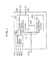
- Fig. 1 shows an image contour tracking apparatus according to the present invention.
- Fig. 2 shows the configuration of an image processing system using an image contour tracking apparatus according to the present invention.
- an image contour tracking apparatus 1 includes a picture element address computation section 100 which computes an address whereby a system processor 2 gains access to an image memory storing an input image therein, a direction code computation section 200 which derives a direction code between the current contour picture element and the next contour picture element, and a computation control section 300 which receives request signals 401 to 403 for the above described modes (1) to (3) and controls the picture element address computation section 100 and the direction code computation section 200.
- the image processing system of Fig. 2 includes a TV camera 5, an A/D converter 4, an image processing processor 6, a system processor 2, an image contour tracking apparatus 1 and an image memory 3.
- FIG. 3 shows transition of picture element address and output direction codes in the case of 4-connectedness and in the case of 8-connectedness.
- the upper left portion of Fig. 3 indicates that a picture element presently in concern (present contour picture element) ⁇ has been retrieved by neighbor search (access in the IMACC mode of (3)) which is represented by an arrow of broken line and which was performed for a picture element previously in concern (previous contour picture element) 0. It also indicates that the direction code from • to ⁇ is 0. And then the center is moved from • to ⁇ .
- the above described Trace mode (1), DIRRD mode (2) and IMACC mode (3) indicate address transitions along the arrows ⁇ ⁇ and -, respectively.
- the direction code points to the direction shown in Fig. 4.
- address changes in the IMACC mode are indicated by direction codes a, ⁇ , ⁇ and a in ( ). Therefore, it is understood that all of the address computations of (1) to (3) can be derived by using the direction codes.
- the address is computed by this method.
- FIG. 5 is broadly divided into an x address (XA) generation section and a Y address (YA) generation section for the image memory.
- the picture element address computation section 100 includes adders 101 and 102, contour tracking start address registers XS 103 and YS 108, a-, ⁇ -, -y-and a-registers 104, 105, 109 and 110 for storing the direction codes representing the displacement components in the X and Y directions with respect to the center picture element, an XT register 106 and a YT register 111 for holding coordinates of the current contour picture element, an XADR register 107 and a YADR register 112 for holding the image memory address in the circular access (IMACC mode) , selectors 113 and 115 for selecting outputs of the contour tracking start address registers XS 103 and YS 108, outputs of the registers XT 106 and YT 111 for
- Figs. 6A and 6B show an example of the circuit of the computation control section 300 and its operation timing chart.
- the computation control section 300 illustrated in Fig. 6A is a circuit for receiving a request of the Trace mode, the DIRRD mode or the IMACC mode from the system processor and for generating control signals 409, 410 and 412 to 415.
- Control signals So and S, supplied via a signal line 410 are signals for controlling the selector 113 and the selector 115 and have logic as listed below.
- the control signal (S,, So) is defined to be (0, 1) so that the registers XT and YT may be selected by the selector 113 and the selector 115.
- the write signals 414 and 415 are generated so that the computation results may be set only in the registers XADR and YADR.
- the control signal (S,, So) is defined to be (1, 0) or (1, 1) so that the registers XADR and YADR may be selected by the selector 113 and the selector 115.
- X of 1 X indicates "1" or "0".
- the write signals 414 and 415 for the registers XADR and YADR are generated.
- the picture element address computation section 100 Upon receiving signals 410 and 412 to 415, the picture element address computation section 100 performs computation in the adder 101 and the adder 102 on the contents of the register selected by the selector 113 and the selector 114 and on the coefficients (a, ⁇ , ⁇ and 5) selected in accordance with control signals 121 and 122 obtained by decoding the direction code 408 supplied from the direction code computation section 200.
- the results of the computation are set into the registers XT, YT, XADR and YADR.
- the contour tracking start address XS and YS (set in registers XS and YS) are set into the registers XT, YT, XADR and YADR.
- the decoder is so controlled as to make B inputs of the adders 101 and 102 zero.
- the coefficient registers a, ⁇ , ⁇ and a are registers for storing therein changes of the picture address in directions, 0, 2, 4 and 6 as shown in Fig. 4.
- contour tracking using a mask of 3 ⁇ 3 can be realized.
- coarse contour tracking with a mask having an arbitrary shape (5 x 5, 3 x 5 or 3 X 7, for example) can be realized. In a uniform pattern, the speed of the contour tracking can be increased.
- the direction code computation section 200 includes an adder 201, a selector (SEL) 202 for selecting either a signal line 405 extending from the system processor 2 or the output of the adder 201, a direction code register DIR 203, and an encoder 204 dor producing the A input data of the adder 201 on the basis of the address computation mode supplied via the signal lines 411.
- SEL selector
- the direction code is computed between the current contour picture element and neighboring picture elements as described with reference to Fig. 3.
- the addition coefficients are changed depending upon the modes Trace, DIRRD and IMACC.
- the direction code of the picture element previously in concern is 4.
- the direction code is already 4 in access to the picture element c.
- the direction code may be obtained by adding 2 to the current direction code. This is in accordance with the known algorithm that search should be performed from the left side of 90° with respect to the traveling direction in case the contour is tracked in the clockwise direction.
- the direction code is obtained by adding -1 in the IMACC mode, 0 in the Trace mode, 1 when the current direction code is an even number in the DIRRD mode, and 2 when the current direction code is an odd number in the DIRRD mode.
- the present embodiment can be used for binary image.
- the present embodiment can be used for gray level image. That is to say, it is also possible to track a picture element having brightness belonging to some range, a picture element which largely changes in brightness from neighbor picture elements, or the like.
Landscapes
- Engineering & Computer Science (AREA)
- Computer Vision & Pattern Recognition (AREA)
- Physics & Mathematics (AREA)
- General Physics & Mathematics (AREA)
- Theoretical Computer Science (AREA)
- Image Analysis (AREA)
- Image Processing (AREA)
Applications Claiming Priority (2)
| Application Number | Priority Date | Filing Date | Title |
|---|---|---|---|
| JP33344/87 | 1987-02-18 | ||
| JP62033344A JPS63201880A (ja) | 1987-02-18 | 1987-02-18 | 画像処理装置 |
Publications (3)
| Publication Number | Publication Date |
|---|---|
| EP0281271A2 true EP0281271A2 (de) | 1988-09-07 |
| EP0281271A3 EP0281271A3 (de) | 1990-06-20 |
| EP0281271B1 EP0281271B1 (de) | 1996-12-04 |
Family
ID=12383948
Family Applications (1)
| Application Number | Title | Priority Date | Filing Date |
|---|---|---|---|
| EP88301299A Expired - Lifetime EP0281271B1 (de) | 1987-02-18 | 1988-02-17 | Bildverarbeitungsverfahren und -gerät |
Country Status (4)
| Country | Link |
|---|---|
| EP (1) | EP0281271B1 (de) |
| JP (1) | JPS63201880A (de) |
| CA (1) | CA1323092C (de) |
| DE (1) | DE3855690T2 (de) |
Cited By (1)
| Publication number | Priority date | Publication date | Assignee | Title |
|---|---|---|---|---|
| GB2257878A (en) * | 1991-07-02 | 1993-01-20 | Hitachi Software Eng | Method for tracing a line image processor |
Families Citing this family (1)
| Publication number | Priority date | Publication date | Assignee | Title |
|---|---|---|---|---|
| JPH08171643A (ja) * | 1994-12-16 | 1996-07-02 | Nec Corp | メッシュ状図形の輪郭抽出方式 |
Family Cites Families (3)
| Publication number | Priority date | Publication date | Assignee | Title |
|---|---|---|---|---|
| JPS5922994B2 (ja) * | 1978-08-11 | 1984-05-30 | 株式会社トキメック | 文字認識装置における輪郭線追跡装置 |
| US4628532A (en) * | 1983-07-14 | 1986-12-09 | Scan Optics, Inc. | Alphanumeric handprint recognition |
| US4575751A (en) * | 1983-11-15 | 1986-03-11 | Rca Corporation | Method and subsystem for plotting the perimeter of an object |
-
1987
- 1987-02-18 JP JP62033344A patent/JPS63201880A/ja active Pending
-
1988
- 1988-02-16 CA CA000558989A patent/CA1323092C/en not_active Expired - Fee Related
- 1988-02-17 DE DE3855690T patent/DE3855690T2/de not_active Expired - Fee Related
- 1988-02-17 EP EP88301299A patent/EP0281271B1/de not_active Expired - Lifetime
Cited By (3)
| Publication number | Priority date | Publication date | Assignee | Title |
|---|---|---|---|---|
| GB2257878A (en) * | 1991-07-02 | 1993-01-20 | Hitachi Software Eng | Method for tracing a line image processor |
| US5384905A (en) * | 1991-07-02 | 1995-01-24 | Hitachi Software Engineering Co., Ltd. | Method for tracing a line image by monitoring the distance between two trace base points |
| GB2257878B (en) * | 1991-07-02 | 1995-04-19 | Hitachi Software Eng | Method for tracing line image in an image processor |
Also Published As
| Publication number | Publication date |
|---|---|
| DE3855690T2 (de) | 1997-06-12 |
| EP0281271A3 (de) | 1990-06-20 |
| JPS63201880A (ja) | 1988-08-19 |
| EP0281271B1 (de) | 1996-12-04 |
| DE3855690D1 (de) | 1997-01-16 |
| CA1323092C (en) | 1993-10-12 |
Similar Documents
| Publication | Publication Date | Title |
|---|---|---|
| KR940006120B1 (ko) | 기준마아크패턴 검출장치 | |
| US5083202A (en) | Motion detector for video signals including a novel line comparison processing scheme | |
| JPH08279049A (ja) | 分割領域の輪郭トレーシング装置 | |
| US4982342A (en) | Image processor system having multifunction look-up table units | |
| JPS646512B2 (de) | ||
| JPH07118784B2 (ja) | テレビジヨン信号の動き検出方法 | |
| US5220615A (en) | Apparatus for and method of hough-converting coordinate data | |
| EP0281271A2 (de) | Bildverarbeitungsverfahren und -gerät | |
| US5400154A (en) | Hybrid interpolation and non-interpolation method and apparatus for image enlarging and contracting | |
| KR940002236B1 (ko) | 영상신호의 2치화 처리장치 | |
| US5345547A (en) | Contour line characteristic point detecting apparatus | |
| JPH04116779A (ja) | データ処理装置 | |
| US4807297A (en) | Neighbor image processing device | |
| JPH10124666A (ja) | テンプレートマッチング処理方法 | |
| JPH0632078B2 (ja) | 画像信号の処理方法 | |
| GB2180118A (en) | Image processing | |
| JP2852257B2 (ja) | イメージデータ回転方法および装置 | |
| JP3004697B2 (ja) | 動きベクトル検出回路 | |
| JPH0496878A (ja) | 画像傾き検出方式 | |
| Toyama et al. | Fast template matching using Brick Partitioning and initial threshold | |
| Agam et al. | Efficient morphological processing of maps and line drawings based on directional interval coding | |
| JPS61260235A (ja) | 画像位置合わせ方式 | |
| JP2835269B2 (ja) | 画像認識装置 | |
| JPH0410113B2 (de) | ||
| JP3092295B2 (ja) | ベクトルデータ編集処理装置 |
Legal Events
| Date | Code | Title | Description |
|---|---|---|---|
| PUAI | Public reference made under article 153(3) epc to a published international application that has entered the european phase |
Free format text: ORIGINAL CODE: 0009012 |
|
| AK | Designated contracting states |
Kind code of ref document: A2 Designated state(s): DE FR GB |
|
| PUAL | Search report despatched |
Free format text: ORIGINAL CODE: 0009013 |
|
| AK | Designated contracting states |
Kind code of ref document: A3 Designated state(s): DE FR GB |
|
| RHK1 | Main classification (correction) |
Ipc: G06F 15/68 |
|
| 17P | Request for examination filed |
Effective date: 19901220 |
|
| 17Q | First examination report despatched |
Effective date: 19930415 |
|
| GRAH | Despatch of communication of intention to grant a patent |
Free format text: ORIGINAL CODE: EPIDOS IGRA |
|
| GRAH | Despatch of communication of intention to grant a patent |
Free format text: ORIGINAL CODE: EPIDOS IGRA |
|
| GRAA | (expected) grant |
Free format text: ORIGINAL CODE: 0009210 |
|
| AK | Designated contracting states |
Kind code of ref document: B1 Designated state(s): DE FR GB |
|
| RHK1 | Main classification (correction) |
Ipc: G06T 5/00 |
|
| REF | Corresponds to: |
Ref document number: 3855690 Country of ref document: DE Date of ref document: 19970116 |
|
| ET | Fr: translation filed | ||
| PLBE | No opposition filed within time limit |
Free format text: ORIGINAL CODE: 0009261 |
|
| STAA | Information on the status of an ep patent application or granted ep patent |
Free format text: STATUS: NO OPPOSITION FILED WITHIN TIME LIMIT |
|
| 26N | No opposition filed | ||
| REG | Reference to a national code |
Ref country code: GB Ref legal event code: IF02 |
|
| PGFP | Annual fee paid to national office [announced via postgrant information from national office to epo] |
Ref country code: FR Payment date: 20030122 Year of fee payment: 16 |
|
| PGFP | Annual fee paid to national office [announced via postgrant information from national office to epo] |
Ref country code: GB Payment date: 20030124 Year of fee payment: 16 |
|
| PGFP | Annual fee paid to national office [announced via postgrant information from national office to epo] |
Ref country code: DE Payment date: 20030310 Year of fee payment: 16 |
|
| PG25 | Lapsed in a contracting state [announced via postgrant information from national office to epo] |
Ref country code: GB Free format text: LAPSE BECAUSE OF NON-PAYMENT OF DUE FEES Effective date: 20040217 |
|
| PG25 | Lapsed in a contracting state [announced via postgrant information from national office to epo] |
Ref country code: DE Free format text: LAPSE BECAUSE OF NON-PAYMENT OF DUE FEES Effective date: 20040901 |
|
| GBPC | Gb: european patent ceased through non-payment of renewal fee |
Effective date: 20040217 |
|
| PG25 | Lapsed in a contracting state [announced via postgrant information from national office to epo] |
Ref country code: FR Free format text: LAPSE BECAUSE OF NON-PAYMENT OF DUE FEES Effective date: 20041029 |
|
| REG | Reference to a national code |
Ref country code: FR Ref legal event code: ST |