EP0281426A2 - Dispositif de circuit électronique pour le diagnostic par exploration de circuits de maintien d'état - Google Patents
Dispositif de circuit électronique pour le diagnostic par exploration de circuits de maintien d'état Download PDFInfo
- Publication number
- EP0281426A2 EP0281426A2 EP88301949A EP88301949A EP0281426A2 EP 0281426 A2 EP0281426 A2 EP 0281426A2 EP 88301949 A EP88301949 A EP 88301949A EP 88301949 A EP88301949 A EP 88301949A EP 0281426 A2 EP0281426 A2 EP 0281426A2
- Authority
- EP
- European Patent Office
- Prior art keywords
- scan
- status
- address
- signal
- circuit
- Prior art date
- Legal status (The legal status is an assumption and is not a legal conclusion. Google has not performed a legal analysis and makes no representation as to the accuracy of the status listed.)
- Granted
Links
Images


Classifications
-
- G—PHYSICS
- G01—MEASURING; TESTING
- G01R—MEASURING ELECTRIC VARIABLES; MEASURING MAGNETIC VARIABLES
- G01R31/00—Arrangements for testing electric properties; Arrangements for locating electric faults; Arrangements for electrical testing characterised by what is being tested not provided for elsewhere
- G01R31/28—Testing of electronic circuits, e.g. by signal tracer
- G01R31/317—Testing of digital circuits
- G01R31/3181—Functional testing
- G01R31/3185—Reconfiguring for testing, e.g. LSSD, partitioning
- G01R31/318533—Reconfiguring for testing, e.g. LSSD, partitioning using scanning techniques, e.g. LSSD, Boundary Scan, JTAG
- G01R31/318569—Error indication, logging circuits
-
- G—PHYSICS
- G01—MEASURING; TESTING
- G01R—MEASURING ELECTRIC VARIABLES; MEASURING MAGNETIC VARIABLES
- G01R31/00—Arrangements for testing electric properties; Arrangements for locating electric faults; Arrangements for electrical testing characterised by what is being tested not provided for elsewhere
- G01R31/28—Testing of electronic circuits, e.g. by signal tracer
- G01R31/317—Testing of digital circuits
- G01R31/3181—Functional testing
- G01R31/3185—Reconfiguring for testing, e.g. LSSD, partitioning
- G01R31/318533—Reconfiguring for testing, e.g. LSSD, partitioning using scanning techniques, e.g. LSSD, Boundary Scan, JTAG
- G01R31/318558—Addressing or selecting of subparts of the device under test
Definitions
- the present invention relates to an electronic circuit device for carrying out a diagnosis of status-holding circuits in the electronic circuit device by scanning.
- a scanning is carried out to read data from status-holding circuits such as latch circuits, flip-flop circuits, and the like, or to write data into these status-holding circuits.
- a parallel scanning method in which a scan address is supplied in parallel to a plurality of address signal lines corresponding to the number of bits of a scan address
- a serial scanning method in which a scan address is supplied successively through a signal line to a serial-parallel converter and converted into a parallel scan address and then fed to a status-holding circuit
- An object of the present invention is to provide an improved electronic circuit device for diagnosing a status-holding circuit by scanning, in which a parallel scan system and a serial scan system are integrated in an electronic circuit device, and accordingly the design of the hardware of the electronic circuit device is optimized when considering whether a sufficient number of terminal pads is available and whether a sufficient space is available for logic circuit elements.
- Another object of the present invention is to utilize the advantages of both a parallel scan system and a serial scan system to enable an increase of the number of elements to be included in an integrated circuit, in the cases where an appreciable number of terminal pads and where only a limited number of terminal pads are provided in the integrated circuit.
- Still another object of the present invention is to integrate a parallel scan system and a serial scan system to increase the freedom of design choice for an electronic circuit device in the form of an integrated circuit.
- the mixed use of serial scanning type and parallel scanning type integrated circuits according to the present invention makes it possible to mount as many circuit elements as possible on an integrated circuit to fully utilize the space of the integrated circuit under the condition of a given number of terminal pads, so that the limitation in design of the large scale integrated circuit device caused by the exclusive unification of the scanning type is eliminated and the total number of the integrated circuits for the large scale integrated circuit device is reduced.
- an electronic circuit device for diagnosing a status-holding circuit by scanning, the device including a first plurality of integrated circuits each including a serial scan circuit and a plurality of status-holding circuits to be scanned, the serial scan circuit receiving serial data, generating an address value of a target status-holding circuit as parallel data from the received serial data, and selecting the target status-holding circuit having the generated address value, and a second plurality of integrated circuits each including a parallel scan circuit and a plurality of status-holding circuits to be scanned, the parallel scan circuit receiving an address value of a target status-holding circuit as parallel data and selecting the target status-holding circuit having the received address value.
- the electronic circuit also includes a serial-parallel converter unit for receiving a serially supplied address signal and converting the received signal into a parallel address signal, a first decoder unit, connected to the serial-parallel converter unit, for decoding a first part of the parallel address signal and providing a plurality of chip select signals each corresponding to one of the first and second plurality of integrated circuits, respectively, a first distributing unit for receiving a second part of the parallel address signal and distributing this second part to each of the second plurality of integrated circuits, and a second distributing unit for receiving the serially supplied address signal and distributing this signal to each of the first plurality of integrated circuits.
- a serial-parallel converter unit for receiving a serially supplied address signal and converting the received signal into a parallel address signal
- a first decoder unit connected to the serial-parallel converter unit, for decoding a first part of the parallel address signal and providing a plurality of chip select signals each corresponding to one of the first and second plurality of integrated
- an electronic circuit device for diagnosing a status-holding circuit by scanning, the device including a first plurality of integrated circuits each including a serial scan circuit and a plurality of status-holding circuits to be scanned, the serial scan circuit receiving serial data, generating an address value of a target status-holding circuit as parallel data from the received serial data, and selecting the target status-holding circuit having the generated address value, and a second plurality of integrated circuits each including a parallel scan circuit and a plurality of status-holding circuits to be scanned, the parallel scan circuit receiving an address value of a target status-holding circuit as parallel data and selecting the target status-holding circuit having the received address value.
- the electronic circuit also includes a parallel-serial converting unit for converting a first part of a supplied parallel address signal into a serial address signal, a first distributing unit for distributing the serial address signal to each of the first plurality of integrated circuits, a first decoder unit for decoding a second part of the supplied parallel address signal and providing a plurality of chip select signal each corresponding to one of the first and second plurality of integrated circuits, respectively, and a second distributing unit for receiving the first part of the supplied parallel address and distributing this first part to each of the second plurality of integrated circuits.
- a parallel-serial converting unit for converting a first part of a supplied parallel address signal into a serial address signal
- a first distributing unit for distributing the serial address signal to each of the first plurality of integrated circuits
- a first decoder unit for decoding a second part of the supplied parallel address signal and providing a plurality of chip select signal each corresponding to one of the first and second plurality of
- the parallel mode scanning instruction portion instructs a parallel scanning for a sequence of integrated circuits having a plurality of status-holding circuits such as latch circuits.
- the serial mode scanning instruction portion instructs a serial scanning for a sequence of integrated circuits having a plurality of status-holding circuits such as latch circuits.
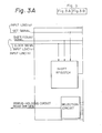
- FIG. 2 A prior art parallel scanning system is shown in Fig. 2.
- the system of Fig. 2 has an integrated circuit (A) which includes an address decoder, a selection circuit, and a plurality of status-holding circuits-1, -2, -3, -4, -5, -6, -7, and -8.
- Each of the status-holding circuits receives a set signal, a reset signal, and an output signal from the address decoder.
- the address decoder receives a selection signal through a plurality of status-holding circuit selection signal lines-1, -2, and -3.
- the number of status-holding circuit selection signal lines is equal to the number of bits which can express a scan address.
- the address decoder is provided and, for example, at least 8 scan address signal lines for scanning 256 status-holding circuits must be provided. This increases the number of terminal pads and thus is disadvantageous.
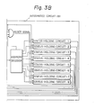
- FIG. 3 A prior art serial scanning system is shown in Fig. 3, the system of Fig. 3 has an integrated circuit (B) which includes a shift register, an address decoder, an AND gate, a selection circuit, and a plurality of status-holding circuits-1, -2, -3, -4, -5, -6, -7, and -8.
- Each of the status-holding circuits receives a set signal, a reset signal, and an output signal from the address decoder.
- the shift register receives input signals, and the output of the shift register is supplied to the address decoder.
- the shift register has a serial/parallel conversion function.
- the AND gate receives a set signal, a shift/count signal, a clock signal, and an output signal from the address decoder, and delivers a reset signal.
- scan address signals are supplied in series through only one set of input lines (a), (b), and (c).
- the shift register holds the successively supplied scan address signals.
- the address decoder receives the output signal of the shift register and generates parallel scan address signals to designate the status-holding circuit to be scanned.
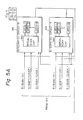
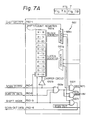
- FIG. 4 An electronic circuit device for diagnosing a status-holding circuit by scanning according to an embodiment of the present invention is shown in Fig. 4.
- a plurality of large scale integrated circuits 61, 63, 64, and 66 are provided, each including status-holding circuits such as latch circuits, and a selector 81.
- the device of Fig. 4 also includes a shifter/counter 21, and decoders 311, and 312, an AND gate 41, and distribution circuits 511, 512, 513, and 514.
- the integrated circuits 66, and 64 are scanned in the serial scan method, the integrated circuits 63, and 61 scanned in the parallel scan method.
- the shifter/counter 21 receives a status holding circuit setting signal, a shift/count signal, and a scan clock signal.
- the output latch address signals S(21-6), S(21-5), S(21-4), and S(21-3) are supplied to the decoder 311, and the output scan address signals S(21-2), S(21-1), and S(21-0) are supplied to the decoder 312.
- the AND gate 41 receives the status holding circuit setting signal, the shift/count signal, the scan clock signal, the signal S(311-0), and the signal S(312-0); the distribution circuit 511 receives the status holding circuit setting signal, the shift/count signal, and the scan clock signal; the distribution circuit 512 receives the output from the AND gate 41; the distribution circuit 513 receives the signal S(311-1); and the distribution circuit 514 receives the signal S(312-1). It should be noted that, in Fig. 4, only one signal lines S(311-1) and S(312-1) are illustrated as the representatives of pluralities of signal lines S(311-1) and S(312-1).
- Each of the integrated circuits 66 and 64 receives the scan-in signal, the shift/count signal, and the scan clock signal from the distribution circuit 511, and each of the integrated circuits 63 and 61 receives the reset signal from the distribution circuit 512, the chip select signal from the distribution circuit 514, the scan-in signal from the distribution circuit 511, and the parallel scan address signal from the distribution circuit 513.
- the shifter/counter 21 operates as a shifter or a counter in accordance with the shift/count signal.
- the shifter/counter 21 operates as a shifter to shift the content of the status hold circuit setting signal.
- the shifter/counter 21 operates as a counter.
- a scan address of any one of the integrated circuit-6, the integrated circuit-4, the integrated circuit-3, and the integrated circuit-1 for which a scan-in or scan-out is desired, is set in outputs S(21-2), S(21-1), and S(21-0) of the shifter/counter 21, and a latch address of the latch circuits in the integrated circuit-6, -4, -3, and -1 is set in the outputs S(21-6), S(21-5), S(21-4), and S(21-3) of the shifter/counter 21.
- the target integrated circuit is the integrated circuit-1
- the target latch circuit is the first latch circuit in the integrated circuit-1
- the shift/count signal is made ON, and the integrated circuit scan address, i.e., chip-select, is set so that the signal S(21-0) is 0, the signal S(21-1) is 0, and the signal S(21-2) is 1; the latch address, i.e., parallel scan address, is set so that the signal S(21-3) is 0, the signal S(21-4) is 0, the signal S(21-5) is 0, and the signal S(21-6) is 1; and, the shift/count signal is made OFF.
- the integrated circuit scan address i.e., chip-select
- the status hold circuit setting signal is made ON, and a rewriting of the latch in the target integrated circuit is carried out. If a scan-out operation is to be carried out, the status hold circuit setting signal is made OFF, the latch in the target integrated circuit is read via a scan-out signal through the selector 81, and the status hold circuit setting signal is distributed to all integrated circuits-6, -4, -3, and -1 as the scan-in signal.
- the signals S(21-2), S(21-1), and S(21-0) from the shifter/counter 21 are distributed to the integrated circuit-1 and the integrated circuit-3 as the chip-select signal via the signal S(312-1) of the decoder 312, to select a single target integrated circuit, the signals S(21-6), S(21-5), S(21-4), and S(21-3) from the shifter/counter 21 are distributed to the latches in the integrated circuit-1 and -3 as the parallel scan address via the signal S(311-1) of the decoder 311, and the signal S(311-0) of the decoder 311 and the signal S(312-0) of the decoder 312 are distributed to the integrated circuit-1 and -3 as the reset signal generation.
- the target integrated circuit is the integrated circuit-6
- the target latch circuit is the eighth latch circuit in the integrated circuit-6
- the signals S(21-6), S(21-5), S(21-4), and S(21-3) from the shifter/counter 21 and the signals from the decoder 311 and the signal from the AND gate 41 exist also in the serial scan circuit 661 (Fig. 6) in the integrated circuit-6.
- the signals of the shifter/counter 21 in the serial scan circuit 661 corresponding to the signals S(21-6), S(21-5), S(21-4), and S(21-3) are set to "0", "0", "0", and "1", respectively, for the address of the target eighth latch circuit, and a scan-in or scan-out operation is carried out.
- one data is selected in the selector 81 based on the signal S(312-2) from the decoder 312 and this one data is read.
- the signals S(312-1) and S(312-2) can be unified as a single signal.
- Each of the integrated circuits 66 and 64 includes a serial scan circuit and a plurality of latch circuits
- each of the integrated circuits 63 and 61 includes a parallel scan circuit and a plurality of latch circuits.
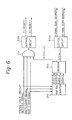
- the structure of a serial scan circuit in an integrated circuit in the device of Fig. 4 is shown in Fig. 6.
- the serial scan circuit includes a shifter/counter 21A, a decoder 311A, an AND gate 41A, a distribution circuit 512A, and a distribution circuit 513A.
- the serial scan circuit includes a shift/count register 661a, a chopper circuit 661b, a decoder 661c, a decoder 661d, and gates 661e, 661f, 661g, and 661h, and terminal pads PAD-1, PAD-7, PAD-8, PAD-9, and PAD-6.
- the output signals from the decoder 661d, the gate 661f, and the gate 661g are supplied to the latch circuits LATCH CKT-1 through LATCH CKT-8 in the integrated circuits (A).
- the PAD-1 receives the chip select signal CHIP SELECT (inverted CHIP SELECT); the PAD-7 receives the scan clock signal SCAN CLOCK ; the PAD-8 receives the scan-in data SCAN-IN DATA ; the PAD-9 receives the shift mode signal SHIFT MODE; and, the PAD-6 delivers the scan-out data SCAN-OUT DATA.
- CHIP SELECT inverted CHIP SELECT
- the PAD-7 receives the scan clock signal SCAN CLOCK
- the PAD-8 receives the scan-in data SCAN-IN DATA
- the PAD-9 receives the shift mode signal SHIFT MODE
- the PAD-6 delivers the scan-out data SCAN-OUT DATA.
- the decoder 661c receives the block address signal from the shift/count register 661a, and the decoder 661d receives the latch address signal from the shift/count register 661a. It should be noted that, in Fig. 7, the output lines of the decoders 661c and 661d are illustrated per one block as the representative of pluralities of the output lines for a plurality of blocks. Also, the output line of the gate 661h is illustrated per one block as the representative of a plurality of the output lines for a plurality of blocks.
- the shift/count register 661a is operated as a shift register, and the scan-in data SCAN-IN DATA received by the PAD-8 is taken bit by bit into the shift/count register 661a based on the scan clock signal SCAN CLOCK .
- the block address is registered in the sections R-8, R-9, and R-10, and the latch address is registered in the sections R-11 through R-18.
- the shift-mode signal SHIFT MODE is "0"
- the shift/count register 661a is operated as a counter, and the scan clock signal SCAN CLOCK is counted.
- the shift/count register 661a first takes the scan-in data, and then operates as a counter, so that the shift/count register 661a carries out successive increments from the scan-in data as the initial value.
- the present integrated circuit (A) When the chip select signal CHIP SELECT is supplied to the PAD-1, the present integrated circuit (A) is selected. When a shift-in of the block address and the latch address for a latch in the present integrated circuit (A) is carried out, this latch is selected so that an input of data into and a take-out of data from this latch can be carried out.
- the RESET signal is generated from the gate 661f.
- the BLOCK SCAN-IN signal is generated from the gate 661g.
- the output of the gate 661e which receives the signals through the PAD-7, PAD-8, and PAD-9 is supplied to the gates 661f and 661g.
- the PAD-8 also can be used for receiving the data to be input to the latch.
- the number of pads of the integrated circuit (A) is greatly reduced, and since usually a great number of integrated circuits is used, the thus enabled reduction of the total number of pads is an advantageous affect.
- the device of Fig. 4 can be expressed as a model shown in Fig. 8.
- the model of Fig. 8 is constituted by a plurality of integrated circuits each having a parallel scan circuit and a plurality of status-holding circuits, a plurality of integrated circuits each having a serial scan circuit and a plurality of status-holding circuits, and a serial/parallel conversion circuit and scan distribution circuit which is connected with a serial scan interface.
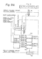
- FIG. 9 An electronic circuit device for diagnosing a status-holding circuit by scanning according to another embodiment of the present invention is shown in Fig. 9.
- the device of Fig. 9 includes a parallel scan address register 22, a counter 23, a selector 24, a selector 25, a decoder 321, a decoder 322, an AND gate 42, and distribution circuits 511, 512, 513, and 514.
- the integrated circuits 66 and 64 are scanned, in series, and the integrated circuits 63 and 61 are scanned in parallel.
- the parallel scan address register 22 receives the scan clock signal and the parallel scan address signal.
- the output signals S(22-6), S(22-5), S(22-4), and S(22-3) are supplied to the decoder 321, and the output signals S(22-2), S(22-1), and S(22-0) are supplied to the decoder 322.
- the counter 23 receives the scan clock signal and the parallel scan mode signal and the selector 24 receives the signal from the counter 23 and the signals S(22-6), S(22-5), S(22-4), and S(22-3).
- the selector 25 selects the status holding circuit and receives the signal from the selector 24, and is controlled by the signal from the counter 23.
- the AND gate 42 receives the signal from the selector 25, the signal from the counter 23, the counter clock signal from the counter 23, an output signal from the decoder 321, and an output signal from the decoder 322;
- the distribution circuit 511 receives the signal from the selector 25, the signal from the counter 23, and the counter clock signal from the counter 23;
- the distribution circuit 512 receives the output from the AND gate 42;
- the distribution circuit 513 receives a signal from the decoder 321; and, the distribution circuit 514 receives a signal from the decoder 322.
- the input signals of the integrated circuits 66, 64, 63, and 61 are similar to those in the device of Fig. 5.
- the parallel scan address having a bit width of, for example, 7 bits, is supplied to the parallel scan address register 22.
- the parallel scan address register 22 is set.
- the counter 23 is operated by the scan clock signal and the parallel scan mode signal.
- the signals S(22-6), S(22-5), S(22-4), and S(22-3) from the parallel scan address register 22 supplied to the selector 24 are selected by the signal from the counter 23 through the selector 24, the selector 25, and the distribution circuit 511 and are transmitted serially as scan-in signals.
- the shift signal is made ON when the value of the counter 23 is not zero.
- the counter clock signal from the counter 23 is distributed as scan clock signals to the integrated circuits which are scanned in series.
- the counter 23 continues to count up until 4 bit signal S(22-6), S(22-5), S(22-4), and S(22-3) is transmitted, and returns to the value zero when this transmission is completed.
- a scan-in operation or a scan-out operation for a single latch circuit in the target integrated circuit which is scanned in series is carried out by the scan-in signal, the shift signal, and the scan clock signal as described above.
Landscapes
- Engineering & Computer Science (AREA)
- General Engineering & Computer Science (AREA)
- Physics & Mathematics (AREA)
- General Physics & Mathematics (AREA)
- Tests Of Electronic Circuits (AREA)
- Test And Diagnosis Of Digital Computers (AREA)
Applications Claiming Priority (4)
| Application Number | Priority Date | Filing Date | Title |
|---|---|---|---|
| JP62051562A JPS63218879A (ja) | 1987-03-06 | 1987-03-06 | シリアルスキヤン制御方式 |
| JP51562/87 | 1987-03-06 | ||
| JP112963/87 | 1987-05-09 | ||
| JP62112963A JP2532092B2 (ja) | 1987-05-09 | 1987-05-09 | 状態保持回路走査方式 |
Publications (3)
| Publication Number | Publication Date |
|---|---|
| EP0281426A2 true EP0281426A2 (fr) | 1988-09-07 |
| EP0281426A3 EP0281426A3 (en) | 1990-04-11 |
| EP0281426B1 EP0281426B1 (fr) | 1996-06-05 |
Family
ID=26392110
Family Applications (1)
| Application Number | Title | Priority Date | Filing Date |
|---|---|---|---|
| EP88301949A Expired - Lifetime EP0281426B1 (fr) | 1987-03-06 | 1988-03-07 | Dispositif de circuit électronique pour le diagnostic par exploration de circuits de maintien d'état |
Country Status (5)
| Country | Link |
|---|---|
| US (1) | US4853929A (fr) |
| EP (1) | EP0281426B1 (fr) |
| AU (1) | AU583203B2 (fr) |
| BR (1) | BR8800993A (fr) |
| DE (1) | DE3855336T2 (fr) |
Families Citing this family (9)
| Publication number | Priority date | Publication date | Assignee | Title |
|---|---|---|---|---|
| US5423050A (en) * | 1991-11-27 | 1995-06-06 | Ncr Corporation | Intermodule test across system bus utilizing serial test bus |
| US5377198A (en) * | 1991-11-27 | 1994-12-27 | Ncr Corporation (Nka At&T Global Information Solutions Company | JTAG instruction error detection |
| US5325368A (en) * | 1991-11-27 | 1994-06-28 | Ncr Corporation | JTAG component description via nonvolatile memory |
| US5343478A (en) * | 1991-11-27 | 1994-08-30 | Ncr Corporation | Computer system configuration via test bus |
| JPH06214821A (ja) * | 1992-03-02 | 1994-08-05 | Motorola Inc | 逐次自己アドレス解読機能を有するデ−タ処理システムとその動作方法 |
| US5875197A (en) * | 1995-05-15 | 1999-02-23 | Motorola Inc. | Addressable serial test system |
| JP2010191849A (ja) * | 2009-02-20 | 2010-09-02 | Renesas Electronics Corp | 状態保持回路及び状態保持方法 |
| US8589867B2 (en) | 2010-06-18 | 2013-11-19 | Microsoft Corporation | Compiler-generated invocation stubs for data parallel programming model |
| US20110314256A1 (en) * | 2010-06-18 | 2011-12-22 | Microsoft Corporation | Data Parallel Programming Model |
Family Cites Families (8)
| Publication number | Priority date | Publication date | Assignee | Title |
|---|---|---|---|---|
| US4244048A (en) * | 1978-12-29 | 1981-01-06 | International Business Machines Corporation | Chip and wafer configuration and testing method for large-scale-integrated circuits |
| AU3230184A (en) * | 1983-08-31 | 1985-03-07 | Amdahl Corporation | Multimode scan apparatus |
| US4701921A (en) * | 1985-10-23 | 1987-10-20 | Texas Instruments Incorporated | Modularized scan path for serially tested logic circuit |
| US4698588A (en) * | 1985-10-23 | 1987-10-06 | Texas Instruments Incorporated | Transparent shift register latch for isolating peripheral ports during scan testing of a logic circuit |
| US4710933A (en) * | 1985-10-23 | 1987-12-01 | Texas Instruments Incorporated | Parallel/serial scan system for testing logic circuits |
| US4710931A (en) * | 1985-10-23 | 1987-12-01 | Texas Instruments Incorporated | Partitioned scan-testing system |
| US4703484A (en) * | 1985-12-19 | 1987-10-27 | Harris Corporation | Programmable integrated circuit fault detection apparatus |
| US4773071A (en) * | 1986-10-02 | 1988-09-20 | Grumman Aerospace Corporation | Memory for storing response patterns in an automatic testing instrument |
-
1988
- 1988-03-04 US US07/164,483 patent/US4853929A/en not_active Expired - Fee Related
- 1988-03-04 AU AU12690/88A patent/AU583203B2/en not_active Ceased
- 1988-03-07 EP EP88301949A patent/EP0281426B1/fr not_active Expired - Lifetime
- 1988-03-07 DE DE3855336T patent/DE3855336T2/de not_active Expired - Fee Related
- 1988-03-07 BR BR8800993A patent/BR8800993A/pt not_active IP Right Cessation
Also Published As
| Publication number | Publication date |
|---|---|
| AU583203B2 (en) | 1989-04-20 |
| AU1269088A (en) | 1988-09-15 |
| BR8800993A (pt) | 1988-10-11 |
| EP0281426A3 (en) | 1990-04-11 |
| DE3855336T2 (de) | 1996-11-07 |
| DE3855336D1 (de) | 1996-07-11 |
| US4853929A (en) | 1989-08-01 |
| EP0281426B1 (fr) | 1996-06-05 |
Similar Documents
| Publication | Publication Date | Title |
|---|---|---|
| US4701916A (en) | Digital integrated circuit with multi-mode register | |
| US5477493A (en) | Semiconductor device having a boundary scan test circuit | |
| EP0549602B1 (fr) | Circuit integré, système et méthode à l'insertion d'erreur | |
| US4931722A (en) | Flexible imbedded test system for VLSI circuits | |
| US4710927A (en) | Diagnostic circuit | |
| KR0163756B1 (ko) | 전자 모듈 소켓장치 | |
| US4377757A (en) | Logic module for integrated digital circuits | |
| EP0868667B1 (fr) | Mode de controle a grande impedance pour circuit jtag | |
| JPS60258593A (ja) | 電子楽器 | |
| GB2391358A (en) | Method of testing and/or debugging a system on chip (SOC) | |
| US4566104A (en) | Testing digital electronic circuits | |
| US4267463A (en) | Digital integrated circuit | |
| EP0281426A2 (fr) | Dispositif de circuit électronique pour le diagnostic par exploration de circuits de maintien d'état | |
| US4933575A (en) | Electric circuit interchangeable between sequential and combination circuits | |
| JP2632731B2 (ja) | 集積回路装置 | |
| KR930011423B1 (ko) | 시험방법, 시험회로 및 시험회로를 갖는 반도체 집적회로 | |
| EP0182358A2 (fr) | Appareil et methode de commande de balayage pour un dispositif de traitement de données | |
| US5495486A (en) | Method and apparatus for testing integrated circuits | |
| EP0498534B1 (fr) | Circuit de génération de configurations de nombres aléatoires artificiels | |
| GB1594066A (en) | Method and arrangement for speeding up the calculation of the address of a microinstruction in a data processing system | |
| GB2121997A (en) | Testing modular data processing systems | |
| EP0196152A2 (fr) | Test de circuits numériques intégrés | |
| US5844921A (en) | Method and apparatus for testing a hybrid circuit having macro and non-macro circuitry | |
| JPS62113075A (ja) | Lsi試験システム | |
| EP0208393A1 (fr) | Tester des circuits intégrés digitaux |
Legal Events
| Date | Code | Title | Description |
|---|---|---|---|
| PUAI | Public reference made under article 153(3) epc to a published international application that has entered the european phase |
Free format text: ORIGINAL CODE: 0009012 |
|
| AK | Designated contracting states |
Kind code of ref document: A2 Designated state(s): DE ES FR GB |
|
| PUAL | Search report despatched |
Free format text: ORIGINAL CODE: 0009013 |
|
| AK | Designated contracting states |
Kind code of ref document: A3 Designated state(s): DE ES FR GB |
|
| 17P | Request for examination filed |
Effective date: 19900622 |
|
| 17Q | First examination report despatched |
Effective date: 19920929 |
|
| GRAA | (expected) grant |
Free format text: ORIGINAL CODE: 0009210 |
|
| AK | Designated contracting states |
Kind code of ref document: B1 Designated state(s): DE ES FR GB |
|
| PG25 | Lapsed in a contracting state [announced via postgrant information from national office to epo] |
Ref country code: FR Effective date: 19960605 Ref country code: ES Free format text: THE PATENT HAS BEEN ANNULLED BY A DECISION OF A NATIONAL AUTHORITY Effective date: 19960605 |
|
| REF | Corresponds to: |
Ref document number: 3855336 Country of ref document: DE Date of ref document: 19960711 |
|
| EN | Fr: translation not filed | ||
| PG25 | Lapsed in a contracting state [announced via postgrant information from national office to epo] |
Ref country code: GB Effective date: 19970307 |
|
| PLBE | No opposition filed within time limit |
Free format text: ORIGINAL CODE: 0009261 |
|
| STAA | Information on the status of an ep patent application or granted ep patent |
Free format text: STATUS: NO OPPOSITION FILED WITHIN TIME LIMIT |
|
| 26N | No opposition filed | ||
| GBPC | Gb: european patent ceased through non-payment of renewal fee |
Effective date: 19970307 |
|
| PGFP | Annual fee paid to national office [announced via postgrant information from national office to epo] |
Ref country code: DE Payment date: 19990315 Year of fee payment: 12 |
|
| PG25 | Lapsed in a contracting state [announced via postgrant information from national office to epo] |
Ref country code: DE Free format text: LAPSE BECAUSE OF NON-PAYMENT OF DUE FEES Effective date: 20010103 |