EP0281743A2 - Objectif détecteur pour microscope à balayage - Google Patents
Objectif détecteur pour microscope à balayage Download PDFInfo
- Publication number
- EP0281743A2 EP0281743A2 EP88100968A EP88100968A EP0281743A2 EP 0281743 A2 EP0281743 A2 EP 0281743A2 EP 88100968 A EP88100968 A EP 88100968A EP 88100968 A EP88100968 A EP 88100968A EP 0281743 A2 EP0281743 A2 EP 0281743A2
- Authority
- EP
- European Patent Office
- Prior art keywords
- lens
- detector
- side electrode
- immersion lens
- source
- Prior art date
- Legal status (The legal status is an assumption and is not a legal conclusion. Google has not performed a legal analysis and makes no representation as to the accuracy of the status listed.)
- Granted
Links
Images


Classifications
-
- H—ELECTRICITY
- H01—ELECTRIC ELEMENTS
- H01J—ELECTRIC DISCHARGE TUBES OR DISCHARGE LAMPS
- H01J37/00—Discharge tubes with provision for introducing objects or material to be exposed to the discharge, e.g. for the purpose of examination or processing thereof
- H01J37/26—Electron or ion microscopes; Electron or ion diffraction tubes
- H01J37/28—Electron or ion microscopes; Electron or ion diffraction tubes with scanning beams
-
- H—ELECTRICITY
- H01—ELECTRIC ELEMENTS
- H01J—ELECTRIC DISCHARGE TUBES OR DISCHARGE LAMPS
- H01J37/00—Discharge tubes with provision for introducing objects or material to be exposed to the discharge, e.g. for the purpose of examination or processing thereof
- H01J37/02—Details
- H01J37/04—Arrangements of electrodes and associated parts for generating or controlling the discharge, e.g. electron-optical arrangement or ion-optical arrangement
- H01J37/10—Lenses
- H01J37/14—Lenses magnetic
- H01J37/141—Electromagnetic lenses
Definitions
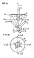
- the scanning electron microscope shown schematically in FIG. 1 essentially consists of an electron beam Generator, preferably a field emission source Q, a condenser lens KL for focusing the primary electrons PE emitted by the cathode K and accelerated in the direction of the anode A into an intermediate image ZP of the electron source lying on the beam axis OA, a lens system (corrector) with at least four eight or Twelve-pole elements KE1 to KE4 for correcting the spherical and chromatic aberrations of the imaging lens, a two-stage deflecting element AE arranged in the beam path immediately behind the corrector KO, each with two cylindrical or plate-shaped structures AE1 and AE2 controlled via signal generators (not shown) and an electrostatic objective lens OL for reducing Imaging of the intermediate image ZP of the source onto the sample PR arranged directly below the objective lens OL on a holder.
- an electron beam Generator preferably a field emission source Q
- a condenser lens KL for focusing the
- the lens system KO designated as a corrector and consisting of at least 4 eight- or twelve-pole elements KE1 to KE4, is from the publications by H. Rose "Electron-Optical Aplanate", Optik 34, Issue 3, 1971 pages 285 to 311 (see in particular page 308 FIG. 9) and H. Koops "Aberration Correction in Electron Microscopy” 9th International Congress on Electron Microscopy, Toronto 1978, Vol 3, pages 185 to 196 (see in particular page 191, FIG. 4). This is arranged in the beam path immediately above the two-stage deflection element AE nete lens system KO is used to correct the opening and color errors of the detector lens OL.
- One of the eight-pole elements KE i (i 1 ...
- d (d + d ) 1/2
- d o denotes the geometrical-optical probe diameter expanded by the Coulomb repulsion of the electrons between the beam generator and the sample (influence of the lateral Boersch effect)
- d F denotes the diameter of the color error disk produced by the color error of the imaging lens.
- a further improvement in the resolution of the scanning electron microscope according to FIG. 1 can therefore be achieved in particular by reducing the lateral and energetic Boersch effect in the beam generator and in the electron-optical column.
- the electrodes of the beam generator K, A and the detector objective OL can be subjected to the following potentials, for example:
Landscapes
- Chemical & Material Sciences (AREA)
- Analytical Chemistry (AREA)
- Physics & Mathematics (AREA)
- Electromagnetism (AREA)
- Analysing Materials By The Use Of Radiation (AREA)
Applications Claiming Priority (2)
| Application Number | Priority Date | Filing Date | Title |
|---|---|---|---|
| DE3703029 | 1987-02-02 | ||
| DE3703029 | 1987-02-02 |
Publications (3)
| Publication Number | Publication Date |
|---|---|
| EP0281743A2 true EP0281743A2 (fr) | 1988-09-14 |
| EP0281743A3 EP0281743A3 (en) | 1990-01-31 |
| EP0281743B1 EP0281743B1 (fr) | 1994-03-30 |
Family
ID=6320041
Family Applications (1)
| Application Number | Title | Priority Date | Filing Date |
|---|---|---|---|
| EP88100968A Expired - Lifetime EP0281743B1 (fr) | 1987-02-02 | 1988-01-22 | Objectif détecteur pour microscope à balayage |
Country Status (4)
| Country | Link |
|---|---|
| US (1) | US4896036A (fr) |
| EP (1) | EP0281743B1 (fr) |
| JP (1) | JPS63221548A (fr) |
| DE (1) | DE3888712D1 (fr) |
Cited By (2)
| Publication number | Priority date | Publication date | Assignee | Title |
|---|---|---|---|---|
| EP0431289A3 (en) * | 1989-12-04 | 1991-11-06 | International Business Machines Corporation | Apparatus for testing samples using charged particles |
| US6949744B2 (en) | 2003-04-17 | 2005-09-27 | Carl Zeiss Nts Gmbh | Electron microscopy system, electron microscopy method and focusing system for charged particles |
Families Citing this family (30)
| Publication number | Priority date | Publication date | Assignee | Title |
|---|---|---|---|---|
| DE4000579A1 (de) * | 1990-01-10 | 1991-07-11 | Integrated Circuit Testing | Ionenstrahlgeraet sowie verfahren zur durchfuehrung von potentialmessungen mittels eines ionenstrahles |
| US5229607A (en) * | 1990-04-19 | 1993-07-20 | Hitachi, Ltd. | Combination apparatus having a scanning electron microscope therein |
| JPH071681B2 (ja) * | 1990-04-19 | 1995-01-11 | 株式会社日立製作所 | 荷電粒子線装置 |
| US5146090A (en) * | 1990-06-11 | 1992-09-08 | Siemens Aktiengesellschaft | Particle beam apparatus having an immersion lens arranged in an intermediate image of the beam |
| JPH071685B2 (ja) * | 1990-09-06 | 1995-01-11 | 株式会社日立製作所 | 走査電子顕微鏡 |
| JP3148353B2 (ja) * | 1991-05-30 | 2001-03-19 | ケーエルエー・インストルメンツ・コーポレーション | 電子ビーム検査方法とそのシステム |
| JP3730263B2 (ja) * | 1992-05-27 | 2005-12-21 | ケーエルエー・インストルメンツ・コーポレーション | 荷電粒子ビームを用いた自動基板検査の装置及び方法 |
| US5789748A (en) * | 1997-05-29 | 1998-08-04 | Stanford University | Low voltage electron beam system |
| DE19828476A1 (de) | 1998-06-26 | 1999-12-30 | Leo Elektronenmikroskopie Gmbh | Teilchenstrahlgerät |
| EP1022766B1 (fr) * | 1998-11-30 | 2004-02-04 | Advantest Corporation | Appareil à faisceau de particules |
| DE69939309D1 (de) * | 1999-03-31 | 2008-09-25 | Advantest Corp | Teilchenstrahlgerät zur schrägen Beobachtung einer Probe |
| US6627886B1 (en) | 1999-05-14 | 2003-09-30 | Applied Materials, Inc. | Secondary electron spectroscopy method and system |
| JP4066078B2 (ja) * | 1999-05-27 | 2008-03-26 | 株式会社ニコン | 写像型電子顕微鏡 |
| US6423976B1 (en) * | 1999-05-28 | 2002-07-23 | Applied Materials, Inc. | Ion implanter and a method of implanting ions |
| JP2003524867A (ja) * | 2000-02-09 | 2003-08-19 | エフ・イ−・アイ・カンパニー | 集束イオンビームシステムのための二次粒子のレンズ通過捕捉 |
| US6960766B2 (en) * | 2000-02-25 | 2005-11-01 | Hermes-Microvision, Inc. | Swinging objective retarding immersion lens electron optics focusing, deflection and signal collection system and method |
| US6392231B1 (en) | 2000-02-25 | 2002-05-21 | Hermes-Microvision, Inc. | Swinging objective retarding immersion lens electron optics focusing, deflection and signal collection system and method |
| US6674075B2 (en) * | 2002-05-13 | 2004-01-06 | Applied Materials, Inc. | Charged particle beam apparatus and method for inspecting samples |
| US6770887B2 (en) * | 2002-07-08 | 2004-08-03 | Ondrej L. Krivanek | Aberration-corrected charged-particle optical apparatus |
| JP4073839B2 (ja) * | 2003-07-22 | 2008-04-09 | 株式会社神戸製鋼所 | 分析装置用磁場発生装置 |
| KR101041661B1 (ko) * | 2003-07-30 | 2011-06-14 | 어플라이드 머티리얼즈 이스라엘 리미티드 | 다중 검출기들을 갖는 스캐닝 전자 현미경 및 다중 검출기기반 이미징을 위한 방법 |
| US7842933B2 (en) * | 2003-10-22 | 2010-11-30 | Applied Materials Israel, Ltd. | System and method for measuring overlay errors |
| DE602005006967D1 (de) * | 2005-03-17 | 2008-07-03 | Integrated Circuit Testing | Analyse-System und Teilchenstrahlgerät |
| US20070090288A1 (en) * | 2005-10-20 | 2007-04-26 | Dror Shemesh | Method and system for enhancing resolution of a scanning electron microscope |
| US20080017811A1 (en) * | 2006-07-18 | 2008-01-24 | Collart Erik J H | Beam stop for an ion implanter |
| JP5280174B2 (ja) * | 2008-12-10 | 2013-09-04 | 日本電子株式会社 | 電子線装置及び電子線装置の動作方法 |
| US9046475B2 (en) | 2011-05-19 | 2015-06-02 | Applied Materials Israel, Ltd. | High electron energy based overlay error measurement methods and systems |
| US9159528B2 (en) | 2013-06-07 | 2015-10-13 | Samsung Electronics Co., Ltd. | Electron beam apparatus |
| US10438769B1 (en) * | 2018-05-02 | 2019-10-08 | Kla-Tencor Corporation | Array-based characterization tool |
| US20240312758A1 (en) * | 2021-06-18 | 2024-09-19 | Asml Netherlands B.V. | System and method for adjusting beam current using a feedback loop in charged particle systems |
Family Cites Families (12)
| Publication number | Priority date | Publication date | Assignee | Title |
|---|---|---|---|---|
| NL7100609A (fr) * | 1970-02-07 | 1971-08-10 | ||
| DE2223367C3 (de) * | 1972-05-12 | 1978-11-30 | Max-Planck-Gesellschaft Zur Foerderung Der Wissenschaften E.V., 3400 Goettingen | Mikrostrahlsonde zur quantitativen Erfassung von geladenen Sekundärteilchen |
| DE2541915A1 (de) * | 1975-09-19 | 1977-03-31 | Max Planck Gesellschaft | Korpuskularstrahlenmikroskop mit ringzonensegmentabbildung |
| US4303864A (en) * | 1979-10-25 | 1981-12-01 | The United States Of America As Represented By The United States Department Of Energy | Sextupole system for the correction of spherical aberration |
| US4590379A (en) * | 1980-09-16 | 1986-05-20 | Martin Frederick W | Achromatic deflector and quadrupole lens |
| US4414474A (en) * | 1982-02-17 | 1983-11-08 | University Patents, Inc. | Corrector for axial aberrations in electron optic instruments |
| WO1984000443A1 (fr) * | 1982-07-16 | 1984-02-02 | Lintech Instr Ltd | Appareil a faisceau electronique et ses collecteurs d'electrons |
| DE3236273A1 (de) * | 1982-09-30 | 1984-04-05 | Siemens AG, 1000 Berlin und 8000 München | Spektrometerobjektiv mit parallelen objektiv- und spektrometerfeldern fuer die potentialmesstechnik |
| DE3236271A1 (de) * | 1982-09-30 | 1984-04-05 | Siemens AG, 1000 Berlin und 8000 München | Spektrometerobjektiv fuer die korpuskularstrahl-messtechnik |
| GB8327737D0 (en) * | 1983-10-17 | 1983-11-16 | Texas Instruments Ltd | Electron detector |
| JPH0736321B2 (ja) * | 1985-06-14 | 1995-04-19 | イーツエーテー、インテグレイテツド、サーキツト、テスチング、ゲゼルシヤフト、フユア、ハルプライタープリユーフテヒニク、ミツト、ベシユレンクテル、ハフツング | 定量的電位測定用スペクトロメ−タ−対物レンズ装置 |
| EP0274622B1 (fr) * | 1986-12-12 | 1990-11-07 | ICT Integrated Circuit Testing Gesellschaft für Halbleiterprüftechnik mbH | Assemblage de détecteur avec un objectif muni d'un détecteur pour instruments à rayons corpusculaires |
-
1988
- 1988-01-22 EP EP88100968A patent/EP0281743B1/fr not_active Expired - Lifetime
- 1988-01-22 DE DE88100968T patent/DE3888712D1/de not_active Expired - Lifetime
- 1988-01-28 JP JP63021141A patent/JPS63221548A/ja active Pending
- 1988-01-29 US US07/150,245 patent/US4896036A/en not_active Expired - Lifetime
Cited By (2)
| Publication number | Priority date | Publication date | Assignee | Title |
|---|---|---|---|---|
| EP0431289A3 (en) * | 1989-12-04 | 1991-11-06 | International Business Machines Corporation | Apparatus for testing samples using charged particles |
| US6949744B2 (en) | 2003-04-17 | 2005-09-27 | Carl Zeiss Nts Gmbh | Electron microscopy system, electron microscopy method and focusing system for charged particles |
Also Published As
| Publication number | Publication date |
|---|---|
| EP0281743B1 (fr) | 1994-03-30 |
| US4896036A (en) | 1990-01-23 |
| DE3888712D1 (de) | 1994-05-05 |
| EP0281743A3 (en) | 1990-01-31 |
| JPS63221548A (ja) | 1988-09-14 |
Similar Documents
| Publication | Publication Date | Title |
|---|---|---|
| EP0281743B1 (fr) | Objectif détecteur pour microscope à balayage | |
| EP0274622B1 (fr) | Assemblage de détecteur avec un objectif muni d'un détecteur pour instruments à rayons corpusculaires | |
| EP0333018B1 (fr) | Lentille d'objectif pour la focalisation de particules chargées | |
| EP0461442B1 (fr) | Appareil à faisceau de particules | |
| DE102018007652B4 (de) | Teilchenstrahl-System sowie Verfahren zur Stromregulierung von Einzel-Teilchenstrahlen | |
| EP0267555B1 (fr) | Objectif de spectromètre pour appareils de mesure par faisceau corpusculaire et procédé pour l'examen d'échantillons. | |
| EP0242602B1 (fr) | Lentille électrostatique et magnétique pour appareils à faisceau corpusculaire | |
| EP0205184B1 (fr) | Objectif de faible aberration comportant un spectromètre de haute acceptance en électrons secondaires | |
| DE69822139T2 (de) | Korrekturvorrichtung zur linsenfehlerkorrektur in ladungsträger-optischen geräten | |
| DE69333184T2 (de) | Abrasterungstechniken in partikelstrahl-vorrichtungen zur minderung von durch oberflächenladungsansammlung hervorgerufenen effekten | |
| DE69822802T2 (de) | Korrigiervorrichtung zur behebung des chromatischen fehlers in korpuskularoptischen geräten | |
| DE112017007063B4 (de) | Ladungsträgerstrahlvorrichtung | |
| DE112016000644B4 (de) | Verbundvorrichtung für geladene Partikelstrahlen | |
| EP0194570A2 (fr) | Microscope corpusculaire à balayage à effet Boersch réduit | |
| EP0218829A2 (fr) | Dispositif détecteur d'électrons secondaires et/ou d'électrons de dispersion en retour dans un appareil à faisceau électronique | |
| DE69920182T2 (de) | Korpuskularstrahloptisches gerät mit auger-elektronendetektion | |
| EP0205185B1 (fr) | Objectif comportant un spectromètre en technique de mesure par faisceau d'électrons | |
| EP0370276A1 (fr) | Dispositif pour détecter des particules chargées secondaires | |
| DE102022120496B4 (de) | Teilchenoptische Anordnung, insbesondere Vielstrahl-Teilchenmikroskop, mit einer Magnetanordnung zum Separieren eines primären und eines sekundären teilchenoptischen Strahlenganges | |
| DE102020123567A1 (de) | Vielzahl-Teilchenstrahl-System mit Kontrast-Korrektur-Linsen-System | |
| EP0348785A2 (fr) | Appareil de mesure par faisceau d'électrons | |
| EP0236807A2 (fr) | Objectif de spectromètre en technique de mesure par faisceau corpusculaire | |
| DE3703028A1 (de) | Rastermikroskop | |
| DE69202782T2 (de) | Feldemissions-Elektronenkanone geringer Aberration. | |
| EP0086431A2 (fr) | Système générateur de faisceau de particules et méthode d'utilisation |
Legal Events
| Date | Code | Title | Description |
|---|---|---|---|
| PUAI | Public reference made under article 153(3) epc to a published international application that has entered the european phase |
Free format text: ORIGINAL CODE: 0009012 |
|
| AK | Designated contracting states |
Kind code of ref document: A2 Designated state(s): DE FR GB IT NL |
|
| PUAL | Search report despatched |
Free format text: ORIGINAL CODE: 0009013 |
|
| AK | Designated contracting states |
Kind code of ref document: A3 Designated state(s): DE FR GB IT NL |
|
| RAP1 | Party data changed (applicant data changed or rights of an application transferred) |
Owner name: ICT INTEGRATED CIRCUIT TESTING GESELLSCHAFT FUER H |
|
| 17P | Request for examination filed |
Effective date: 19900622 |
|
| 17Q | First examination report despatched |
Effective date: 19921204 |
|
| GRAA | (expected) grant |
Free format text: ORIGINAL CODE: 0009210 |
|
| AK | Designated contracting states |
Kind code of ref document: B1 Designated state(s): DE FR GB IT NL |
|
| ITF | It: translation for a ep patent filed | ||
| REF | Corresponds to: |
Ref document number: 3888712 Country of ref document: DE Date of ref document: 19940505 |
|
| GBT | Gb: translation of ep patent filed (gb section 77(6)(a)/1977) |
Effective date: 19940511 |
|
| ET | Fr: translation filed | ||
| PLBE | No opposition filed within time limit |
Free format text: ORIGINAL CODE: 0009261 |
|
| STAA | Information on the status of an ep patent application or granted ep patent |
Free format text: STATUS: NO OPPOSITION FILED WITHIN TIME LIMIT |
|
| 26N | No opposition filed | ||
| REG | Reference to a national code |
Ref country code: GB Ref legal event code: IF02 |
|
| PG25 | Lapsed in a contracting state [announced via postgrant information from national office to epo] |
Ref country code: IT Free format text: LAPSE BECAUSE OF NON-PAYMENT OF DUE FEES;WARNING: LAPSES OF ITALIAN PATENTS WITH EFFECTIVE DATE BEFORE 2007 MAY HAVE OCCURRED AT ANY TIME BEFORE 2007. THE CORRECT EFFECTIVE DATE MAY BE DIFFERENT FROM THE ONE RECORDED. Effective date: 20050122 |
|
| PGFP | Annual fee paid to national office [announced via postgrant information from national office to epo] |
Ref country code: GB Payment date: 20061213 Year of fee payment: 20 |
|
| PGFP | Annual fee paid to national office [announced via postgrant information from national office to epo] |
Ref country code: NL Payment date: 20061222 Year of fee payment: 20 |
|
| PGFP | Annual fee paid to national office [announced via postgrant information from national office to epo] |
Ref country code: DE Payment date: 20070131 Year of fee payment: 20 |
|
| REG | Reference to a national code |
Ref country code: GB Ref legal event code: PE20 |
|
| NLV7 | Nl: ceased due to reaching the maximum lifetime of a patent |
Effective date: 20080122 |
|
| PG25 | Lapsed in a contracting state [announced via postgrant information from national office to epo] |
Ref country code: NL Free format text: LAPSE BECAUSE OF EXPIRATION OF PROTECTION Effective date: 20080122 |
|
| PGFP | Annual fee paid to national office [announced via postgrant information from national office to epo] |
Ref country code: FR Payment date: 20070103 Year of fee payment: 20 |
|
| PG25 | Lapsed in a contracting state [announced via postgrant information from national office to epo] |
Ref country code: GB Free format text: LAPSE BECAUSE OF EXPIRATION OF PROTECTION Effective date: 20080121 |