EP0282023A2 - Dispositif de mémoire à semi-conducteur - Google Patents
Dispositif de mémoire à semi-conducteur Download PDFInfo
- Publication number
- EP0282023A2 EP0282023A2 EP88103704A EP88103704A EP0282023A2 EP 0282023 A2 EP0282023 A2 EP 0282023A2 EP 88103704 A EP88103704 A EP 88103704A EP 88103704 A EP88103704 A EP 88103704A EP 0282023 A2 EP0282023 A2 EP 0282023A2
- Authority
- EP
- European Patent Office
- Prior art keywords
- gate
- floating gate
- erase
- memory device
- semiconductor memory
- Prior art date
- Legal status (The legal status is an assumption and is not a legal conclusion. Google has not performed a legal analysis and makes no representation as to the accuracy of the status listed.)
- Granted
Links
- 239000004065 semiconductor Substances 0.000 title claims abstract description 30
- 238000007667 floating Methods 0.000 claims abstract description 102
- 239000012535 impurity Substances 0.000 claims abstract description 44
- 229910021420 polycrystalline silicon Inorganic materials 0.000 claims description 39
- 229920005591 polysilicon Polymers 0.000 claims description 37
- 239000000758 substrate Substances 0.000 claims description 12
- OAICVXFJPJFONN-UHFFFAOYSA-N Phosphorus Chemical compound [P] OAICVXFJPJFONN-UHFFFAOYSA-N 0.000 claims description 10
- 229910052698 phosphorus Inorganic materials 0.000 claims description 10
- 239000011574 phosphorus Substances 0.000 claims description 10
- RQNWIZPPADIBDY-UHFFFAOYSA-N arsenic atom Chemical compound [As] RQNWIZPPADIBDY-UHFFFAOYSA-N 0.000 claims description 8
- 229910052785 arsenic Inorganic materials 0.000 claims description 7
- 150000004767 nitrides Chemical class 0.000 claims 2
- 239000010410 layer Substances 0.000 description 45
- VYPSYNLAJGMNEJ-UHFFFAOYSA-N Silicium dioxide Chemical compound O=[Si]=O VYPSYNLAJGMNEJ-UHFFFAOYSA-N 0.000 description 27
- 229910052814 silicon oxide Inorganic materials 0.000 description 27
- 238000000034 method Methods 0.000 description 9
- 229910052581 Si3N4 Inorganic materials 0.000 description 8
- HQVNEWCFYHHQES-UHFFFAOYSA-N silicon nitride Chemical compound N12[Si]34N5[Si]62N3[Si]51N64 HQVNEWCFYHHQES-UHFFFAOYSA-N 0.000 description 8
- 230000008569 process Effects 0.000 description 7
- 238000004519 manufacturing process Methods 0.000 description 6
- 230000005684 electric field Effects 0.000 description 5
- 238000007254 oxidation reaction Methods 0.000 description 5
- 230000001590 oxidative effect Effects 0.000 description 5
- 239000000243 solution Substances 0.000 description 4
- 230000007423 decrease Effects 0.000 description 3
- 125000004437 phosphorous atom Chemical group 0.000 description 3
- 230000001133 acceleration Effects 0.000 description 2
- XAGFODPZIPBFFR-UHFFFAOYSA-N aluminium Chemical compound [Al] XAGFODPZIPBFFR-UHFFFAOYSA-N 0.000 description 2
- 229910052782 aluminium Inorganic materials 0.000 description 2
- -1 arsenic ions Chemical class 0.000 description 2
- 238000005229 chemical vapour deposition Methods 0.000 description 2
- 230000003247 decreasing effect Effects 0.000 description 2
- 238000009792 diffusion process Methods 0.000 description 2
- 239000002784 hot electron Substances 0.000 description 2
- 230000006872 improvement Effects 0.000 description 2
- 238000005468 ion implantation Methods 0.000 description 2
- 238000001020 plasma etching Methods 0.000 description 2
- 230000009467 reduction Effects 0.000 description 2
- 241001663154 Electron Species 0.000 description 1
- XUIMIQQOPSSXEZ-UHFFFAOYSA-N Silicon Chemical compound [Si] XUIMIQQOPSSXEZ-UHFFFAOYSA-N 0.000 description 1
- 230000009471 action Effects 0.000 description 1
- 230000002411 adverse Effects 0.000 description 1
- 230000015572 biosynthetic process Effects 0.000 description 1
- 239000000969 carrier Substances 0.000 description 1
- 238000001312 dry etching Methods 0.000 description 1
- 230000006870 function Effects 0.000 description 1
- 238000002347 injection Methods 0.000 description 1
- 239000007924 injection Substances 0.000 description 1
- 238000009413 insulation Methods 0.000 description 1
- 239000011229 interlayer Substances 0.000 description 1
- 150000002500 ions Chemical class 0.000 description 1
- 230000007246 mechanism Effects 0.000 description 1
- 230000003647 oxidation Effects 0.000 description 1
- 229910052710 silicon Inorganic materials 0.000 description 1
- 239000010703 silicon Substances 0.000 description 1
- 239000002356 single layer Substances 0.000 description 1
- 230000002311 subsequent effect Effects 0.000 description 1
- 239000000126 substance Substances 0.000 description 1
Images


Classifications
-
- H—ELECTRICITY
- H10—SEMICONDUCTOR DEVICES; ELECTRIC SOLID-STATE DEVICES NOT OTHERWISE PROVIDED FOR
- H10D—INORGANIC ELECTRIC SEMICONDUCTOR DEVICES
- H10D84/00—Integrated devices formed in or on semiconductor substrates that comprise only semiconducting layers, e.g. on Si wafers or on GaAs-on-Si wafers
- H10D84/01—Manufacture or treatment
- H10D84/0123—Integrating together multiple components covered by H10D12/00 or H10D30/00, e.g. integrating multiple IGBTs
- H10D84/0126—Integrating together multiple components covered by H10D12/00 or H10D30/00, e.g. integrating multiple IGBTs the components including insulated gates, e.g. IGFETs
- H10D84/0135—Manufacturing their gate conductors
-
- H—ELECTRICITY
- H10—SEMICONDUCTOR DEVICES; ELECTRIC SOLID-STATE DEVICES NOT OTHERWISE PROVIDED FOR
- H10D—INORGANIC ELECTRIC SEMICONDUCTOR DEVICES
- H10D30/00—Field-effect transistors [FET]
- H10D30/60—Insulated-gate field-effect transistors [IGFET]
- H10D30/68—Floating-gate IGFETs
- H10D30/681—Floating-gate IGFETs having only two programming levels
- H10D30/684—Floating-gate IGFETs having only two programming levels programmed by hot carrier injection
- H10D30/685—Floating-gate IGFETs having only two programming levels programmed by hot carrier injection from the channel
Definitions
- This invention relates to a semiconductor memory device into which data can be electrically written and in which data can be electrically erased. In particular, this invention relates to a semiconductor memory device wherein the data stored in all memory cells can be erased simultaneously.
- a flash type electrical erasable programmable read only memory (FE2PROM) with a function to electrically erase all of the stored bits in a simultaneous manner is known as disclosed in USP Nos. 4,437,172 and 4,466,081.
- the FE2PROM as disclosed in these patents allows the stored data to be electrically and simultaneously erased on all of the bit lines. With this advantageous feature, the FE2PROM has progressively superseded the UV type EPROM in which the data stored therein is erased by ultraviolet rays.
- FIG. 1 An example of one of the memory cells constituting the FE2PROM is illustrated in cross sectional form in Fig. 1.
- reference numeral 30 designates a p-type semiconductor substrate.
- Field oxide film 31 is layered on substrate 30, and erase gate 32, acting as a first polysilicon layer, is partially layered on field oxidation film 31.
- Reference numeral 33 indicates a gate oxide film.
- Floating gate 34 is layered on gate oxide film 33, and consists of a second polysilicon layer. The end portion of floating gate 34 is overlaid on the end portion of erase gate 32, with silicon oxide film 35 interlayered between them. Silicon oxide film 35 serves as an insulating film and is formed by oxidizing erase gate 32.
- Control gate 37 which serves as a third polysilicon layer, is layered over floating gate 34, with silicon oxide film 36 interlayered between them. Silicon oxide film 36 serves as an insulating film and is formed by oxidizing floating gate 34. Although not shown, source and drain regions as N type diffusion layers are provided on substrate 30, and located at sides of floating gate 34, respectively. An interlayer insulating film (not shown) is layered on control gate 37, and has contact holes opened to the source and drain regions, and the surfaces of erase gate 32 and control gate 37. Within each contact hole is formed a lead electrode made of aluminum.
- the data write operation of the FE2PROM with the memory cells thus structured is similar to that of the conventional EPROM. Specifically, a high voltage is applied to the drain region (not shown) of the memory cell, and control gate 37. The applied high voltage causes hot electrons in the channel region located under floating gate 34. The generated hot electrons are injected into the floating gate 34 as set at a predetermined potential, because the high voltage has been applied to control gate 37. The injection of electrons into floating gate 34 increases the threshold voltage in the channel region.
- a high voltage is applied to erase gate 32, to place the silicon oxide film 35 between erase gate 32 and floating gate 34 in a high electric field.
- the electrons which have been already injected into floating gate 34 are discharged into erase gate 32.
- the threshold voltage in the channel region decreases, and the data is erased.
- a fixed voltage is applied to the drain region and control gate 37.
- the memory cells into which the data have been written and whose channel regions have increased threshold voltage are in an off state.
- Those memory cells whose data have erased and channel region have decreased threshold voltage are in an on state.
- the on- and off-states are read out in the form of logical "1" and "0" of the data, respectively.
- the erasure characteristic of this cell depends on the quality and thickness of silicon oxide film 35, and the shapes of floating gate 34 and erase gate 32, which are separated by silicon oxide film 35.
- the thickness of silicon oxide film 35 is thin, an insulation of silicon oxide film 35 is reduced by appropriately selecting a way of process for erase gate 32 and a method of forming silicon oxide film 35.
- FE2PROM the cause for the erroneous data write has been known and will be described.
- a high voltage is applied to control gate 37 and the drain.
- the same substrate further contains other memory cells which are not in the write mode, but whose control gates 37 are applied with the same high voltage.
- the potential at floating gate 34 is pulled to a high potential level, so that an electric field is developed between floating gate 34 and erase gate 32.
- an irregularity called asperity
- the leak current flowing from the first polysilicon layer having a surface of small asperity to the second polysilicon layer having a surface of great asperity is larger than the leak current flowing from the second polysilicon layer to the first polysilicon layer. In other words, more electrons move from the second to the first polysilicon layer than the first to the second polysilicon layer.
- the asperity on the upper surface of erase gate 32 is larger than that on the lower surface of floating gate 34. Therefore, electrons may be injected into floating gate 34, through silicon oxide film 35 existing between erase gate 32 and floating gate 34. In this way, the erroneous data write is caused by injecting electrons into the floating gates of those memory cells which are not in the write mode.
- the memory cell as shown in sectional form in Fig. 2 has been proposed.
- the first polysilicon layer constitutes floating gate 34.
- a second polysilicon layer forms an erase gate 32.
- Insulating film 38 existing between between erase gate 32 and control gate 37 is formed by oxidizing the polysilicon of erase gate 32.
- erase gate 32 and control gate 37 are used to conductive layer respectively.
- the polysilicon layers constituting the erase gate and the control gate are doped with impurity, for example, phosphorus atoms or arsenic atoms at 6 x 10²⁰/cm3 or more of concentration, viz., at a concentration of the solution limit.
- the polysilicon layer forming floating gate 34 is doped with phosphorus atoms or arsenic atoms at a concentration of the solution limit. Therefore, a degree of asperity occurring on the upper surface of floating gate 34 is small.
- a leak current caused between floating gate 34 and erase gate 32 in the erroneous write direction is nearly equal to that in the erasure direction.
- the erroneous write characteristic and the erasure characteristic are both improved unsatisfactorily.
- an object of this invention is to provide a semiconductor memory device with the improved erroneous write characteristic and erasure characteristic.
- a semiconductor memory device having a semiconductor substrate of a first conductivity type, a floating gate containing impurity at a predetermined concentration layered on a first insulating film which also is layered on the substrate, an erase gate above the floating gate, with a second insulating film interlaid therebetween, a part of said erase gate overlapping with said floating gate, and said erase gate containing impurity at a predetermined concentration, and a control gate layered above said floating gate with a third insulating film interlaid therebetween, wherein an impurity concentration in at least the part of floating gate overlapping the erase gate is lower than that of the erase gate.
- FIG. 3 A group of memory cells used for a semiconductor memory device according to this invention is shown in Fig. 3.
- FIG. 4 A cross section of the memory cell taken on line I - I ⁇ is shown in Fig. 4.
- reference numeral 10 designates a silicon semiconductor substrate of p-type.
- Field oxide film 11 for separating the adjacent memory cells from one another is formed on substrate 10.
- Gate oxide film 12 is formed on a specific location of substrate 10 which correspond to a channel region in the element region as separated by field oxide film 11.
- Floating gate 13 as a first polysilicon layer is formed on gate oxide film 12. Both ends of floating gate 13 extend over field oxide film 11.
- Erase gate 15 as a second polysilicon layer is laid above one end of floating gate 13 with silicon oxide film 14 interlaid therebetween.
- Silicon oxide film 14 serves as an insulating film and is formed by oxidizing the polysilicon layer of floating gate 13.
- Erase gate 15 overlaps with the end portions of floating gate 13 of two adjacent memory cells as viewed horizontally in Fig. 3.
- Three-layered 16 is layered over floating gate 13 and erase gate 15.
- Control gate 17 consisting of a third polysilicon layer is continuously layered over the three layered film 16.
- Three-layered film 16 consists of first silicon oxide (SiO2) film 16A as a bottom layer, second silicon nitride (Si3N4) film 16B as a medium layer, and a third silicon oxide (SiO2) film 16C as a top layer.
- Source region 18 and drain region 19 as n-type diffusion layers are formed on the element region surfaces located at both sides of floating gate 13, respectively.
- Source region 18 is a single layer and used in common for all of the memory cells.
- Interlaying insulating film 20 is laid on control gate 17.
- Conductive layer 21 made of aluminum, for example, is formed on interlaying insulating film 20. Conductive layer 21 is connected to the drain region 19 of each memory cell, through contact hole 22.
- Erase gate 15 and control gate 17 are incorporated in each memory cell, and these are used as interconnection layers.
- the polysilicon layers of the erase gate 15 and control gate 17 are doped with impurity, for example, phosphorus atoms or arsenic atoms at 6 x 10²⁰/cm3 or more, i.e., a concentration equal or approximate to the solution limit.
- impurity for example, phosphorus atoms or arsenic atoms at 6 x 10²⁰/cm3 or more, i.e., a concentration equal or approximate to the solution limit.
- the same type of impurity is also doped into the first layer polysilicon layer of floating gate 13.
- the same type of impurity is doped into the region 13A of floating gate 13 laid under erase gate 15.
- the impurity concentration is much lower than that for erase gate 15 and control gate 17, and less than 6 x 10²⁰/cm3 for example, in a range from 1 x 10²⁰/cm3 to 4 x 10²⁰/cm3.
- the region 13B of floating gate 13 not overlapping with erase gate 15 is doped with the same type of impurity at the same concentration as that of erase gate 15 and control gate erase 17, i.e., 6 x 10²⁰/cm3.
- Silicon oxide film 14 laid over floating gate 13 is formed by oxidizing the polysilicon layer of floating gate 13.
- the polysilicon layer satisfactorily doped with impurity at the concentration on the level of the solution limit is then oxidized, so that the asperity appearing on the surface is remarkably lessened.
- the impurity concentration is less than 6 x 10²⁰/cm3
- the asperity rapidly increases on the surface of the polysilicon layer, after it is subjected to the subsequent oxidization process. It is estimated that the rapid increase of asperity is due to the fact that since the impurity concentration of the polysilicon layer is not uniform in the layer, the oxidization rate is not constant over the surface of the polysilicon layer.
- the asperity on the surface of the region 13A of floating gate 13 overlapping with erase gate 15 increase. Therefore, a concentration of an electric field occurs in the region 13A.
- a accelerated electric field make it easy to generate the leak current between floating gate 13 and erase gate 15.
- the electric field is weaker than that in the flat area of region 13B.
- the leak current flows from floating gate 13 to erase gate 15 increases. In other words, when considering the electrons action, the electrons flow is enhanced in the direction from floating gate 13 toward erase gate 15, resulting in improvement of the erasure characteristic of the memory device.
- a graph of Fig. 5 comparatively shows leak current characteristics between the floating gate and the erase gate of the conventional memory cell and the memory cell of this embodiment.
- Curves "a”, “b” and “c” indicate variations of the leak current when a voltage V FE is applied to those gates, with its positive polarity at the erase gate. These curves “a”, “b” and “c” are for the impurity (phosphorus) concentrations of the region 13A, 6 x 10²⁰/cm3, 4 x 10²⁰/cm3, and 2 x 10²⁰/cm3, respectively. Further, curve “a” is the leak current variation of the conventional memory cell. Curves “b” and “c” show the leak current variation of the memory cells according to this embodiment.
- Curves 1, 2 and 3 indicate variations of the leak current when a voltage V FE is applied to those gates, with its positive polarity at the floating gate. These curves 1, 2 and 3 are for the impurity (phosphorus) concentrations of the region 13A, 6 x 10²⁰/cm3, 4 x 10²⁰/cm3, and 2 x 10²⁰/cm3, respectively. Further, curve 1 is the leak current variation of the conventional memory cell. Curves 2 and 3 show the leak current variation of the memory cells according to this embodiment.
- the leak current flowing from the erase gate to the floating gate becomes large.
- the leak current in this direction contributes to the discharge of electrons from the floating gate to the erase gate.
- the erasure characteristic can be improved by reducing the impurity concentration in the region 13A.
- the leak current flowing from the floating gate to the erase gate increases a little, while electrons move in this direction is impeded.
- This directional leak current contributes to the erroneous write operation in which electrons are injected into the floating gate.
- the increase of the leak current is small, and hence the occurrence of the erroneous write operation is limited.
- Fig. 6 shows characteristic curves, which describe variations of the leak current between the floating gate and the erase gate.
- the abscissa of the graph represents a concentration (/cm3) of impurity (phosphorus) in the region 13A of floating gate 13.
- the ordinate represents a leak current (A).
- characteristic curve I indicates a variation of a leak current flowing from erase gate 15 to floating gate 13, when a voltage of 25 V is applied to between erase gate 15 and floating gate 13.
- erase gate 15 is set at the positive polarity of the applied voltage.
- This curve shows that the leak current increases with reduction of the impurity concentration of the region 13A of floating gate 13.
- the increased leak current provides an improved erasure characteristic.
- Characteristic curve II indicates a variation of a leak current flowing from floating gate 13 to erase gate 15, when a voltage of 25 V is applied to between floating gate 13 and erase gate 15. In this case, floating gate 13 is set at the positive polarity of the applied voltage. This curve II shows that the leak current increases a little when the impurity concentration in the region 13A is decreased.
- filed oxide film 11 is formed on substrate 10.
- the first polysilicon layer is deposited thereon.
- Appropriate impurity such as phosphorus or arsenic are diffused into the polysilicon layer.
- the first polysilicon layer is patterned by reactive ion etching process (RIE), to form floating gate 13.
- RIE reactive ion etching process
- the structure is thermally oxidized in a condition that it is placed at 1000°C and for 30 minutes in gas containing O2 and N2 or O2 and Ar with the proportion of 2 to 8. As the result of this thermal oxidization, silicon oxide film 14, 350 Angstroms thick, is formed on the surface of floating gate 13.
- a second polysilicon layer is deposited over the surface of the structure.
- Phosphorus or arsenic impurity at 6 x 10²⁰/cm3 is diffused into the second polysilicon layer.
- the second polysilicon layer is patterned by chemical dry etching (CDE) process, to form erase gate 15.
- CDE chemical dry etching
- the structure is thermally oxidized in a condition that it is placed at 1000°C and for 30 minutes in gas containing 02 and N2 or O2 and Ar with the proportion of 5 to 5.
- silicon oxide film 16A 400 Angstroms thick, is formed over floating gate 13 and erase gate 15.
- Silicon nitride film 16B of 150 Angstroms in thickness is then formed over silicon oxide film 16A by chemical vapor deposition (CVD) process at 700°C and for 20 minutes.
- the structure is placed in a wet atmosphere and thermally oxidized at 1000°C and for 50 minutes, to form silicon oxide film 16C of 50 Angstroms in thickness on the surface of silicon nitride film 16B.
- a third polysilicon layer is deposited and doped with phosphorus or arsenic impurity at 6 x 10²⁰/cm3 or more, and then is patterned, to form control gate 17.
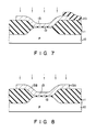
- the process steps to reduce the impurity concentration in the region 13A of floating gate 13 follows. Reference is made to Fig. 7 for this description. Following the steps to form field oxide film 11 and gate oxide film 12, the first polysilicon layer is deposited over the entire surface of the structure. Then, the first polysilicon layer is patterned to form floating gate 13. Subsequently, the portion to be used as region 13A is selectively covered with ion implanting mask 23 made of photo register, for example. Phosphorus or arsenic ions are implanted into floating gate 13 at a predetermined acceleration voltage and a predetermined dosage, by ion implantation process.
- the acceleration voltage and dosage must be selected so that the impurity concentration of region 13A is in a range from 1 x 10²⁰/cm3 to 4 x 10²⁰/cm3, and that in region 13B is 6 x 10²⁰/cm3 or more.
- the concentration in the region 13A of floating gate 13 is set within the range from 1 x 10²⁰/cm3 to 4 x 10²⁰/cm3, and that in region 13B is 6 x 10²⁰/cm3 or more.
- the impurity concentration in the region 13A of floating gate 13 of each memory cell is set to be equal to that in region 13B.
- the exact value of the concentration is 1 x 10²⁰/cm3 to 4 x 10²⁰/cm3, which is lower than 6 x 10²⁰/cm3 of erase gate 15.
- This embodiment also attains the impurity concentration relationships of the region 13B of floating gate 13 and erase gate 15, which is comparable with that of the first embodiment. Therefore, the satisfactory improvement of the erasure characteristic and production yield can be expected.
- a first reason for this is that the three-layered film has a lower density of the weak spots contained in the insulating film than the single insulating film.
- a second reason resides in the current mechanism peculiar to the three-layered film.
- a number of carriers generated when the leak current is caused are electrons in silicon oxide film 16A or 16C of the three-layered film, and these are holes in silicon nitride film 16B.
- the leak current is caused in silicon nitride film 16B either when hole current is easy to flow due to the weak spots or when electron current is easy to flow in silicon nitride film. Since there is a rare case that both currents flow simultaneously, the leak current flowing from control gate 17 toward floating gate 13 will never be increased.
Landscapes
- Non-Volatile Memory (AREA)
- Semiconductor Memories (AREA)
Applications Claiming Priority (2)
| Application Number | Priority Date | Filing Date | Title |
|---|---|---|---|
| JP58109/87 | 1987-03-13 | ||
| JP62058109A JPH0640587B2 (ja) | 1987-03-13 | 1987-03-13 | 半導体記憶装置 |
Publications (3)
| Publication Number | Publication Date |
|---|---|
| EP0282023A2 true EP0282023A2 (fr) | 1988-09-14 |
| EP0282023A3 EP0282023A3 (en) | 1989-05-17 |
| EP0282023B1 EP0282023B1 (fr) | 1992-06-10 |
Family
ID=13074805
Family Applications (1)
| Application Number | Title | Priority Date | Filing Date |
|---|---|---|---|
| EP88103704A Expired - Lifetime EP0282023B1 (fr) | 1987-03-13 | 1988-03-09 | Dispositif de mémoire à semi-conducteur |
Country Status (4)
| Country | Link |
|---|---|
| EP (1) | EP0282023B1 (fr) |
| JP (1) | JPH0640587B2 (fr) |
| KR (1) | KR910007375B1 (fr) |
| DE (1) | DE3871823T2 (fr) |
Cited By (5)
| Publication number | Priority date | Publication date | Assignee | Title |
|---|---|---|---|---|
| EP0282022A3 (fr) * | 1987-03-13 | 1989-05-17 | Kabushiki Kaisha Toshiba | Dispositif de mémoire à semi-conducteur |
| US5162247A (en) * | 1988-02-05 | 1992-11-10 | Emanuel Hazani | Process for trench-isolated self-aligned split-gate EEPROM transistor and memory array |
| US5166904A (en) * | 1988-02-05 | 1992-11-24 | Emanuel Hazani | EEPROM cell structure and architecture with increased capacitance and with programming and erase terminals shared between several cells |
| US5303185A (en) * | 1988-02-05 | 1994-04-12 | Emanuel Hazani | EEPROM cell structure and architecture with increased capacitance and with programming and erase terminals shared between several cells |
| US5332914A (en) * | 1988-02-05 | 1994-07-26 | Emanuel Hazani | EEPROM cell structure and architecture with increased capacitance and with programming and erase terminals shared between several cells |
Families Citing this family (2)
| Publication number | Priority date | Publication date | Assignee | Title |
|---|---|---|---|---|
| KR910005235B1 (ko) * | 1988-12-01 | 1991-07-24 | 재단법인 한국화학연구소 | 흡수성 고분자 물질 및 그의 제조방법 |
| JP2679389B2 (ja) * | 1990-10-12 | 1997-11-19 | 日本電気株式会社 | 不揮発性半導体記憶セルのデータ消去方法 |
Family Cites Families (5)
| Publication number | Priority date | Publication date | Assignee | Title |
|---|---|---|---|---|
| EP0054355B1 (fr) * | 1980-12-08 | 1986-04-16 | Kabushiki Kaisha Toshiba | Dispositif semiconducteur à mémoire |
| EP0053878B1 (fr) * | 1980-12-08 | 1985-08-14 | Kabushiki Kaisha Toshiba | Dispositif semiconducteur à mémoire |
| JPS61136274A (ja) * | 1984-12-07 | 1986-06-24 | Toshiba Corp | 半導体装置 |
| JPS61225872A (ja) * | 1985-03-29 | 1986-10-07 | Nippon Denso Co Ltd | 半導体不揮発性記憶装置の製造方法 |
| JPH0640588B2 (ja) * | 1987-03-13 | 1994-05-25 | 株式会社東芝 | 半導体記憶装置 |
-
1987
- 1987-03-13 JP JP62058109A patent/JPH0640587B2/ja not_active Expired - Fee Related
-
1988
- 1988-03-09 EP EP88103704A patent/EP0282023B1/fr not_active Expired - Lifetime
- 1988-03-09 DE DE8888103704T patent/DE3871823T2/de not_active Expired - Lifetime
- 1988-03-12 KR KR1019880002643A patent/KR910007375B1/ko not_active Expired
Cited By (5)
| Publication number | Priority date | Publication date | Assignee | Title |
|---|---|---|---|---|
| EP0282022A3 (fr) * | 1987-03-13 | 1989-05-17 | Kabushiki Kaisha Toshiba | Dispositif de mémoire à semi-conducteur |
| US5162247A (en) * | 1988-02-05 | 1992-11-10 | Emanuel Hazani | Process for trench-isolated self-aligned split-gate EEPROM transistor and memory array |
| US5166904A (en) * | 1988-02-05 | 1992-11-24 | Emanuel Hazani | EEPROM cell structure and architecture with increased capacitance and with programming and erase terminals shared between several cells |
| US5303185A (en) * | 1988-02-05 | 1994-04-12 | Emanuel Hazani | EEPROM cell structure and architecture with increased capacitance and with programming and erase terminals shared between several cells |
| US5332914A (en) * | 1988-02-05 | 1994-07-26 | Emanuel Hazani | EEPROM cell structure and architecture with increased capacitance and with programming and erase terminals shared between several cells |
Also Published As
| Publication number | Publication date |
|---|---|
| JPH0640587B2 (ja) | 1994-05-25 |
| JPS63224366A (ja) | 1988-09-19 |
| DE3871823T2 (de) | 1992-12-10 |
| EP0282023B1 (fr) | 1992-06-10 |
| KR910007375B1 (ko) | 1991-09-25 |
| EP0282023A3 (en) | 1989-05-17 |
| KR880011928A (ko) | 1988-10-31 |
| DE3871823D1 (de) | 1992-07-16 |
Similar Documents
| Publication | Publication Date | Title |
|---|---|---|
| US6673677B2 (en) | Method for manufacturing a multi-bit memory cell | |
| US5449941A (en) | Semiconductor memory device | |
| KR940006094B1 (ko) | 불휘발성 반도체 기억장치 및 그 제조방법 | |
| US5629541A (en) | Semiconductor memory device constituted by single transistor type non-volatile cells and facilitated for both electrical erasing and writing of data | |
| US4996572A (en) | Semiconductor memory device | |
| JP3973819B2 (ja) | 半導体記憶装置およびその製造方法 | |
| US5352620A (en) | Method of making semiconductor device with memory cells and peripheral transistors | |
| JPH03181178A (ja) | 不揮発性半導体記憶装置 | |
| JPH05218451A (ja) | 不揮発性半導体記憶装置およびその製造方法 | |
| US20050189582A1 (en) | Charge trapping memory cell and fabrication method | |
| US4918501A (en) | Semiconductor device and method of producing the same | |
| USRE37959E1 (en) | Semiconductor integrated circuit device and method of manufacturing the same | |
| US5643812A (en) | Method of making EEPROM flash memory cell with erase gate | |
| US5194924A (en) | Semiconductor device of an LDD structure having a floating gate | |
| EP0282023B1 (fr) | Dispositif de mémoire à semi-conducteur | |
| US6551867B1 (en) | Non-volatile semiconductor memory device and method for manufacturing the same | |
| US5252846A (en) | Semiconductor memory device with an improved erroneous write characteristic and erasure characteristic | |
| JPH07130885A (ja) | 半導体記憶装置およびその製造方法 | |
| EP0298430A2 (fr) | Dispositif semi-conducteur à grille flottante | |
| US7462529B2 (en) | Nonvolatile memory device for storing multi-bit data | |
| JPH11238815A (ja) | 不揮発性半導体記憶装置およびその製造方法 | |
| JP3430086B2 (ja) | 不揮発性半導体記憶装置およびその製造方法 | |
| JP2004342852A (ja) | 半導体記憶装置及びその製造方法、半導体装置、携帯電子機器、並びにicカード | |
| JP3389003B2 (ja) | 不揮発性半導体記憶装置及びその製造方法 | |
| JP2007067043A (ja) | 半導体装置およびその製造方法 |
Legal Events
| Date | Code | Title | Description |
|---|---|---|---|
| PUAI | Public reference made under article 153(3) epc to a published international application that has entered the european phase |
Free format text: ORIGINAL CODE: 0009012 |
|
| 17P | Request for examination filed |
Effective date: 19880309 |
|
| AK | Designated contracting states |
Kind code of ref document: A2 Designated state(s): DE FR GB |
|
| PUAL | Search report despatched |
Free format text: ORIGINAL CODE: 0009013 |
|
| AK | Designated contracting states |
Kind code of ref document: A3 Designated state(s): DE FR GB |
|
| 17Q | First examination report despatched |
Effective date: 19911011 |
|
| GRAA | (expected) grant |
Free format text: ORIGINAL CODE: 0009210 |
|
| AK | Designated contracting states |
Kind code of ref document: B1 Designated state(s): DE FR GB |
|
| REF | Corresponds to: |
Ref document number: 3871823 Country of ref document: DE Date of ref document: 19920716 |
|
| ET | Fr: translation filed | ||
| PLBE | No opposition filed within time limit |
Free format text: ORIGINAL CODE: 0009261 |
|
| STAA | Information on the status of an ep patent application or granted ep patent |
Free format text: STATUS: NO OPPOSITION FILED WITHIN TIME LIMIT |
|
| 26N | No opposition filed | ||
| PGFP | Annual fee paid to national office [announced via postgrant information from national office to epo] |
Ref country code: GB Payment date: 19980302 Year of fee payment: 11 |
|
| PGFP | Annual fee paid to national office [announced via postgrant information from national office to epo] |
Ref country code: DE Payment date: 19980313 Year of fee payment: 11 |
|
| PG25 | Lapsed in a contracting state [announced via postgrant information from national office to epo] |
Ref country code: GB Free format text: LAPSE BECAUSE OF NON-PAYMENT OF DUE FEES Effective date: 19990309 |
|
| REG | Reference to a national code |
Ref country code: FR Ref legal event code: D6 |
|
| GBPC | Gb: european patent ceased through non-payment of renewal fee |
Effective date: 19990309 |
|
| PG25 | Lapsed in a contracting state [announced via postgrant information from national office to epo] |
Ref country code: DE Free format text: LAPSE BECAUSE OF NON-PAYMENT OF DUE FEES Effective date: 20000101 |
|
| PGFP | Annual fee paid to national office [announced via postgrant information from national office to epo] |
Ref country code: FR Payment date: 20070308 Year of fee payment: 20 |