EP0282281A2 - Differenzierender logischer Schaltkreis für asynchrone Systeme - Google Patents
Differenzierender logischer Schaltkreis für asynchrone Systeme Download PDFInfo
- Publication number
- EP0282281A2 EP0282281A2 EP88302042A EP88302042A EP0282281A2 EP 0282281 A2 EP0282281 A2 EP 0282281A2 EP 88302042 A EP88302042 A EP 88302042A EP 88302042 A EP88302042 A EP 88302042A EP 0282281 A2 EP0282281 A2 EP 0282281A2
- Authority
- EP
- European Patent Office
- Prior art keywords
- input
- gate
- receiving
- output
- signal
- Prior art date
- Legal status (The legal status is an assumption and is not a legal conclusion. Google has not performed a legal analysis and makes no representation as to the accuracy of the status listed.)
- Withdrawn
Links
Images



Classifications
-
- H—ELECTRICITY
- H03—ELECTRONIC CIRCUITRY
- H03K—PULSE TECHNIQUE
- H03K19/00—Logic circuits, i.e. having at least two inputs acting on one output; Inverting circuits
-
- H—ELECTRICITY
- H03—ELECTRONIC CIRCUITRY
- H03K—PULSE TECHNIQUE
- H03K19/00—Logic circuits, i.e. having at least two inputs acting on one output; Inverting circuits
- H03K19/20—Logic circuits, i.e. having at least two inputs acting on one output; Inverting circuits characterised by logic function, e.g. AND, OR, NOR, NOT circuits
-
- H—ELECTRICITY
- H03—ELECTRONIC CIRCUITRY
- H03K—PULSE TECHNIQUE
- H03K5/00—Manipulating of pulses not covered by one of the other main groups of this subclass
- H03K5/153—Arrangements in which a pulse is delivered at the instant when a predetermined characteristic of an input signal is present or at a fixed time interval after this instant
- H03K5/1534—Transition or edge detectors
Definitions
- the present invention is directed to a differentiating circuit for asynchronous systems and, more particularly to a self-clocking, self-timing differentiating circuit for digital asynchronous systems which can be used alone as a differentiating circuit or in combination with other circuits to form AND, OR, etc. logical circuits having a differentiated signal output.
- Boolean algebra is frequently used to specify the states entered by logical circuits by means of tables that indicate output values in connection with inputs for combinatorial networks, and also to specify inside states for sequential networks.
- the representation is a description of "steady" variables, as if the elements that perform the logical operations were ideal elements lacking any physical feature whatever.
- the physical parameters that "deviate” from the ideal behavior of these circuits must also be considered.
- the usual methods for implementation of digital circuits takes into account such deviating parameters in a merely “statistical" manner, without considering the variables of interest during signal transitions, since under this circumstance they would assume values generally defined as arbitrary.
- a "clock" element is typically used which enables the circuit to settle for the necessary time in order that the transients caused by the various transit times, particularly of physical devices, may expire.
- the clock enables the operations to occur in orderly fashion by connecting the timing with only the stable circuit conditions evoked by Boolean algebra so that transient arbitrary values are not used.
- circuits which utilize signals from a logic circuit may use signals having transient variations.
- the concept of variation is, however, tied to the mathematical concept of the first derivative of the variable as compared with time.
- the time constraint represented by the presence of the clock may be overcome by means of a differentiating circuit which operates under the condition that the signal, which represents the derivative of the variable, continues to exist until the user of the meaning of the occurred signal variation has utilized it as required.
- This is accomplished by introducing into the differentiation circuit a feedback signal which is generated when a circuit receiving the derivative signal of the differentiation circuit utilizes that derivative signal.
- the feedback signal is used to disable the derivative signal. This will be the "minimum time" associated with the time derivative. A shorter time might not let the derivative assume any meaning, since the derivative signal might not have been utilized by the user.
- a DERIVER circuit for asynchronous systems which has at least one input signal of a ----------- variable (X), a derivative output signal (Y) produced by a change in state of the input signal(s) (X) and a feedback input signal (F) which controls how long the derivative output is available to a circuit which utilizes it.
- DERIVER is a class of circuits that perform any logical function, be it simple or complex, both combinatorial and sequential, at different integration grades and that utilize both positive and negative logics, and which control the duration of the existence of derivative output signal by a feedback signal from a circuit which utilizes the derivative output signal.
- Fig. 1 represents the block diagram of a ⁇ X DERIVER 11 placed in an environment of use.
- Fig. 2 shows the time representation of signal variations in accordance with the invention associated with the Fig. 1 DERIVER circuit, which may be summarized as follows: "only the variation (0 ⁇ 1) of variable X produces an equivalent variation (0 ⁇ 1) of variable Y. This occurs independently from the state of feedback variable F. Only the variation (0 ⁇ 1) of variable F which occurs when the derivative signal Y is used by a downstream utilization circuit 15 will cause the variable Y to return to its rest state, i.e., (1 ⁇ 0). Now the DERIVER circuit is ready for the next operation. It is clear that variable X on which the differentiating operation is performed will have to remain steady during the operation itself.
- a feedback signal E (0 ⁇ 1) heading back to the source 13 of signals to the DERIVER circuit ⁇ X can be easily obtained from the same DERIVER; it is the complement of output signal Y.
- the signal E from the ⁇ X DERIVER is the feedback signal to the source S.
- Fig. 3 The logical signal table for the Fig. 1 DERIVER is represented in Fig. 3, while Fig. 4 illustrates the schematic diagram of the DERIVER 11.
- the Fig. 4 embodiment includes an AND gate 21 which receives the input signal X and an output signal P from NAND gate 23 which is one of two NAND gates (23, 25) cross-coupled to form a flip-flop. Another input to NAND gate 23 is taken from the output of NAND gate 25, which receives as its inputs, the signal P and the output of a NAND gate 27. NAND gate 27 receives as inputs thereto, the feedback signal F and the S output of NAND gate 29, which is one of two NAND gates (29, 31) cross-coupled to form another flip-flop. NAND gate 29, receives at its inputs, the feedback signal F and the output of NAND gate 31, and NAND gate 31 in turn receives as its input the signal Y and the signal S. An inverter 33 also receives the signal Y and provides an inverted signal Y as the signal E.
- Fig. 5 shows the complete timing diagram for the Fig. 4 circuit.
- this device namely, the generation of the derivative signal Y in connection with the significant transition applied to input signal X, is fully independent from the current state of feedback signal F; disabling of the derivative signal Y (1 ⁇ 0) will occur only through a significant transition (0 ⁇ 1) of the feedback signal F.
- DERIVER circuits constructed in accordance with the invention in their elementary form, can be considered as having two separate parts: the first one is the logical operator that is an AND gate (e.g., gate 21) in the case of non-inverting DERIVER; the second part is an RS flip-flop (e.g., formed by gates 23, 25) that has the function of memorizing the inside state of the DERIVER.
- the first one is the logical operator that is an AND gate (e.g., gate 21) in the case of non-inverting DERIVER;
- the second part is an RS flip-flop (e.g., formed by gates 23, 25) that has the function of memorizing the inside state of the DERIVER.
- Fig. 4 depicts a first type of DERIVER constructed in accordance with the invention, while the simplified circuit of Fig. 6 depicts a second type.
- the Fig. 9 circuit represents yet a third type of DERIVER.
- a DERIVER circuit of the invention can use the feedback signal in different ways, the first type generate the output signal Y in full independence from the feedback signal (Fig. 4) while the second and the third (Fig. 6, 9) generate the output signal Y depending on the status of the feedback signal F, but, in any event, all circuits share the characteristic that the active transition of the feedback signal F is needed to return the output signal Y to a rest state (1 ⁇ 0).
- the function of a NOT DERIVER ( ⁇ NOT) is obtained by complementing the DERIVER Y output signal, using an inverter.
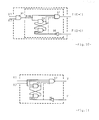
- the logical function will be realized by either placing before the DERIVER an ordinary AND circuit 41, as shown in Fig. 10, or realizing the function inside the DERIVER itself, as shown in Fig.11.
- the input signals x 1... x n are applied to respective inputs of AND gate 67 and NAND gate 63, the latter of which is cross-coupled with NAND gate 65 to produce a flip-flop.
- NAND gate 65 also receives the feedback signal F through inverter 35.
- AND gate 67 also receives as an input, the output P of NAND gate 63.
- the two input signals X1, X2 are respectively applied to NAND gates 73 and 75 and to respective inputs of AND gates 83 and 85, NAND gates 73 and 75 also receive as an input thereto, the output of NAND gate 61, which in turn receives as input signals, the outputs of NAND gates 73 and 75 and inverter 35 (for the feedback signal F).
- AND gate 83 also receives the output of gate 73 and inverter 35, while AND gate 85 also receives the output signals from gate 75 and inverter 35.
- NAND and NOR are obviously obtained by logical negation of the output of the AND and OR DERIVERS herein described, for example, by adding an inverter to the output of the circuits shown in Figs. 10-13.
- a DERIVER in accordance with the invention in its form of a Boolean differentiating network operator has two parts: the first one assumes the structure of the function to be performed, such as derivative, NOT, AND, OR as well as the combination of the same, while the second part, namely the flip-flop (formed by gates 23, 25) for the feedback state memorization, remains substantially unchanged.
- DERIVERS which form part of the present invention can also be constructed to perform --- complex functions, for example XOR, by adding logical gates to perform such function, e.g., XOR, to any of the three types of DERIVERS discussed above with respect to Figs. 4, 6 and 9, in the manner described above for Figs. 10, 11, 12 and 13 for the AND and OR functions.
Landscapes
- Physics & Mathematics (AREA)
- Engineering & Computer Science (AREA)
- Computer Hardware Design (AREA)
- Computing Systems (AREA)
- General Engineering & Computer Science (AREA)
- Mathematical Physics (AREA)
- Nonlinear Science (AREA)
- Logic Circuits (AREA)
- Dc Digital Transmission (AREA)
- Manipulation Of Pulses (AREA)
Applications Claiming Priority (2)
| Application Number | Priority Date | Filing Date | Title |
|---|---|---|---|
| IT19648/87A IT1204915B (it) | 1987-03-11 | 1987-03-11 | Derivatori per sistemi asincronici |
| IT1964887 | 1987-03-11 |
Publications (2)
| Publication Number | Publication Date |
|---|---|
| EP0282281A2 true EP0282281A2 (de) | 1988-09-14 |
| EP0282281A3 EP0282281A3 (de) | 1989-11-08 |
Family
ID=11160068
Family Applications (1)
| Application Number | Title | Priority Date | Filing Date |
|---|---|---|---|
| EP88302042A Withdrawn EP0282281A3 (de) | 1987-03-11 | 1988-03-09 | Differenzierender logischer Schaltkreis für asynchrone Systeme |
Country Status (9)
| Country | Link |
|---|---|
| US (1) | US4943744A (de) |
| EP (1) | EP0282281A3 (de) |
| JP (1) | JPS6453621A (de) |
| KR (1) | KR880012010A (de) |
| AU (1) | AU596735B2 (de) |
| BR (1) | BR8801057A (de) |
| IL (1) | IL85677A (de) |
| IT (1) | IT1204915B (de) |
| ZA (1) | ZA881659B (de) |
Families Citing this family (3)
| Publication number | Priority date | Publication date | Assignee | Title |
|---|---|---|---|---|
| IT1204621B (it) * | 1987-05-15 | 1989-03-10 | Montedison Spa | Circuito flip-flop rs asincrono con scatto comandato dalle transizioni applicate agli ingressi |
| US5225723A (en) * | 1990-05-24 | 1993-07-06 | Apple Computer, Inc. | Circuitry for the timing data output enable pulses |
| EP0644342A4 (de) | 1993-03-30 | 1996-10-09 | Thk Co Ltd | Führungseinheit für linearbewegungen und verfahren zu deren zusammenbau. |
Family Cites Families (12)
| Publication number | Priority date | Publication date | Assignee | Title |
|---|---|---|---|---|
| US3792362A (en) * | 1972-10-30 | 1974-02-12 | Amdahl Corp | Clock apparatus and data processing system |
| US4321484A (en) * | 1979-02-28 | 1982-03-23 | International Business Machines Corporation | Field effect transistor multivibrator |
| FR2497427A1 (fr) * | 1980-12-29 | 1982-07-02 | Chazenfus Henri | Circuit de reglage du rapport cyclique d'un signal periodique impulsionnel et dispositif multiplicateur de frequence par 2, incluant ce circuit de reglage |
| US4425514A (en) * | 1981-11-10 | 1984-01-10 | Rca Corporation | Fixed pulse width, fast recovery one-shot pulse generator |
| US4423338A (en) * | 1982-03-01 | 1983-12-27 | International Business Machines Corporation | Single shot multivibrator having reduced recovery time |
| US4620118A (en) * | 1982-10-01 | 1986-10-28 | At&T Bell Laboratories | Dual port access circuit with automatic asynchronous contention resolving capability |
| US4502014A (en) * | 1982-11-24 | 1985-02-26 | Rca Corporation | Coincident pulse cancelling circuit |
| US4607173A (en) * | 1984-03-14 | 1986-08-19 | At&T Bell Laboratories | Dual-clock edge triggered flip-flop circuits |
| US4638189A (en) * | 1984-06-29 | 1987-01-20 | Monolithic Memories, Incorporated | Fast and gate with programmable output polarity |
| EP0228156A3 (de) * | 1985-11-07 | 1989-06-07 | Control Data Corporation | Prüfsystem für VLSI-Schaltungen |
| US4700187A (en) * | 1985-12-02 | 1987-10-13 | Concurrent Logic, Inc. | Programmable, asynchronous logic cell and array |
| US4685103A (en) * | 1985-12-24 | 1987-08-04 | Gte Communication Systems Corporation | Control circuit for a centrex attendant console interface |
-
1987
- 1987-03-11 IT IT19648/87A patent/IT1204915B/it active
-
1988
- 1988-03-08 AU AU12802/88A patent/AU596735B2/en not_active Ceased
- 1988-03-08 ZA ZA881659A patent/ZA881659B/xx unknown
- 1988-03-09 IL IL85677A patent/IL85677A/xx unknown
- 1988-03-09 EP EP88302042A patent/EP0282281A3/de not_active Withdrawn
- 1988-03-10 BR BR8801057A patent/BR8801057A/pt unknown
- 1988-03-10 JP JP63057345A patent/JPS6453621A/ja active Pending
- 1988-03-10 KR KR1019880002461A patent/KR880012010A/ko not_active Withdrawn
-
1989
- 1989-12-14 US US07/449,428 patent/US4943744A/en not_active Expired - Fee Related
Non-Patent Citations (1)
| Title |
|---|
| PHOENIX CONFERENCE ON COMPUTERS AND COMMUNICATIONS, Scottsdale, Arizona, 26th-28th March 1986, pages 662-673, The Institute of Electrical and Electronics Engineers, Inc., New York, US; D.C. KIRKPATRICK et al.: "An asynchronous design style to achieve ultimate operating speed" * |
Also Published As
| Publication number | Publication date |
|---|---|
| IL85677A0 (en) | 1988-08-31 |
| IT1204915B (it) | 1989-03-10 |
| AU1280288A (en) | 1988-09-15 |
| EP0282281A3 (de) | 1989-11-08 |
| BR8801057A (pt) | 1988-10-18 |
| US4943744A (en) | 1990-07-24 |
| IL85677A (en) | 1991-12-12 |
| KR880012010A (ko) | 1988-10-31 |
| AU596735B2 (en) | 1990-05-10 |
| ZA881659B (en) | 1988-10-26 |
| IT8719648A0 (it) | 1987-03-11 |
| JPS6453621A (en) | 1989-03-01 |
Similar Documents
| Publication | Publication Date | Title |
|---|---|---|
| Eichelberger | Hazard detection in combinational and sequential switching circuits | |
| US4748417A (en) | Method and circuit arrangement for switching a clock-controlled device having a plurality of operating statuses | |
| US4287437A (en) | Method and circuitry for equalizing the differing delays of semiconductor chips | |
| GB1581864A (en) | Logic systems | |
| JPH0758609A (ja) | グリッチ抑制回路及び方法 | |
| US4389723A (en) | High-speed pattern generator | |
| JPS63228206A (ja) | クロツク分配方式 | |
| US4943744A (en) | Differentiating logical circuit for asynchronous systems | |
| US5185537A (en) | Gate efficient digital glitch filter for multiple input applications | |
| US3380033A (en) | Computer apparatus | |
| US2942192A (en) | High speed digital data processing circuits | |
| JPS6010910A (ja) | ラツチ回路アレイ | |
| CA1274002A (en) | Event distribution and combination system | |
| EP0298747A2 (de) | Register | |
| EP0237680A2 (de) | Ereignisverteilungs- und -kombinationssystem | |
| US4140872A (en) | Control system for functional sequences | |
| Chiang et al. | Hazard-free design of mixed operating mode asynchronous sequential circuits | |
| JPH04306013A (ja) | ラッチ回路装置 | |
| Borriello | Synthesis of mixed synchronous/asynchronous control logic | |
| US3060328A (en) | Commutator utilizing only flip-flops and coincidence circuits | |
| EP0817087A2 (de) | Implementierung synchroner Hochgeschwindigkeitsautomaten mit kurzen Datenvorbereitungs- und Haltezeiten | |
| US5349620A (en) | Timer access control apparatus | |
| US5615241A (en) | Programmable rate generator | |
| KR920000698Y1 (ko) | 클럭 소스 선택시 글리치 제거회로 | |
| JPH0789145B2 (ja) | リセット信号発生回路を備える電子装置 |
Legal Events
| Date | Code | Title | Description |
|---|---|---|---|
| PUAI | Public reference made under article 153(3) epc to a published international application that has entered the european phase |
Free format text: ORIGINAL CODE: 0009012 |
|
| AK | Designated contracting states |
Kind code of ref document: A2 Designated state(s): AT BE CH DE ES FR GB IT LI NL SE |
|
| 17P | Request for examination filed |
Effective date: 19890126 |
|
| PUAL | Search report despatched |
Free format text: ORIGINAL CODE: 0009013 |
|
| AK | Designated contracting states |
Kind code of ref document: A3 Designated state(s): AT BE CH DE ES FR GB IT LI NL SE |
|
| 17Q | First examination report despatched |
Effective date: 19910731 |
|
| STAA | Information on the status of an ep patent application or granted ep patent |
Free format text: STATUS: THE APPLICATION IS DEEMED TO BE WITHDRAWN |
|
| 18D | Application deemed to be withdrawn |
Effective date: 19911211 |