EP0282961A2 - Onduleur pour alimenter une charge avec composante inductive - Google Patents
Onduleur pour alimenter une charge avec composante inductive Download PDFInfo
- Publication number
- EP0282961A2 EP0282961A2 EP88104049A EP88104049A EP0282961A2 EP 0282961 A2 EP0282961 A2 EP 0282961A2 EP 88104049 A EP88104049 A EP 88104049A EP 88104049 A EP88104049 A EP 88104049A EP 0282961 A2 EP0282961 A2 EP 0282961A2
- Authority
- EP
- European Patent Office
- Prior art keywords
- winding
- voltage
- transistor
- inverter according
- transistors
- Prior art date
- Legal status (The legal status is an assumption and is not a legal conclusion. Google has not performed a legal analysis and makes no representation as to the accuracy of the status listed.)
- Granted
Links
Images


Classifications
-
- H—ELECTRICITY
- H02—GENERATION; CONVERSION OR DISTRIBUTION OF ELECTRIC POWER
- H02M—APPARATUS FOR CONVERSION BETWEEN AC AND AC, BETWEEN AC AND DC, OR BETWEEN DC AND DC, AND FOR USE WITH MAINS OR SIMILAR POWER SUPPLY SYSTEMS; CONVERSION OF DC OR AC INPUT POWER INTO SURGE OUTPUT POWER; CONTROL OR REGULATION THEREOF
- H02M7/00—Conversion of AC power input into DC power output; Conversion of DC power input into AC power output
- H02M7/42—Conversion of DC power input into AC power output without possibility of reversal
- H02M7/44—Conversion of DC power input into AC power output without possibility of reversal by static converters
- H02M7/48—Conversion of DC power input into AC power output without possibility of reversal by static converters using discharge tubes with control electrode or semiconductor devices with control electrode
- H02M7/505—Conversion of DC power input into AC power output without possibility of reversal by static converters using discharge tubes with control electrode or semiconductor devices with control electrode using devices of a thyratron or thyristor type requiring extinguishing means
- H02M7/515—Conversion of DC power input into AC power output without possibility of reversal by static converters using discharge tubes with control electrode or semiconductor devices with control electrode using devices of a thyratron or thyristor type requiring extinguishing means using semiconductor devices only
-
- H—ELECTRICITY
- H05—ELECTRIC TECHNIQUES NOT OTHERWISE PROVIDED FOR
- H05B—ELECTRIC HEATING; ELECTRIC LIGHT SOURCES NOT OTHERWISE PROVIDED FOR; CIRCUIT ARRANGEMENTS FOR ELECTRIC LIGHT SOURCES, IN GENERAL
- H05B6/00—Heating by electric, magnetic or electromagnetic fields
- H05B6/02—Induction heating
- H05B6/06—Control, e.g. of temperature, of power
- H05B6/062—Control, e.g. of temperature, of power for cooking plates or the like
-
- H—ELECTRICITY
- H02—GENERATION; CONVERSION OR DISTRIBUTION OF ELECTRIC POWER
- H02M—APPARATUS FOR CONVERSION BETWEEN AC AND AC, BETWEEN AC AND DC, OR BETWEEN DC AND DC, AND FOR USE WITH MAINS OR SIMILAR POWER SUPPLY SYSTEMS; CONVERSION OF DC OR AC INPUT POWER INTO SURGE OUTPUT POWER; CONTROL OR REGULATION THEREOF
- H02M7/00—Conversion of AC power input into DC power output; Conversion of DC power input into AC power output
- H02M7/42—Conversion of DC power input into AC power output without possibility of reversal
- H02M7/44—Conversion of DC power input into AC power output without possibility of reversal by static converters
- H02M7/48—Conversion of DC power input into AC power output without possibility of reversal by static converters using discharge tubes with control electrode or semiconductor devices with control electrode
- H02M7/53—Conversion of DC power input into AC power output without possibility of reversal by static converters using discharge tubes with control electrode or semiconductor devices with control electrode using devices of a triode or transistor type requiring continuous application of a control signal
- H02M7/537—Conversion of DC power input into AC power output without possibility of reversal by static converters using discharge tubes with control electrode or semiconductor devices with control electrode using devices of a triode or transistor type requiring continuous application of a control signal using semiconductor devices only, e.g. single switched pulse inverters
- H02M7/538—Conversion of DC power input into AC power output without possibility of reversal by static converters using discharge tubes with control electrode or semiconductor devices with control electrode using devices of a triode or transistor type requiring continuous application of a control signal using semiconductor devices only, e.g. single switched pulse inverters in a push-pull configuration
Definitions
- the invention relates to an inverter which generates an alternating voltage for a consumer with an inductive component, in particular for the coil in an inductive hotplate, from a direct voltage.
- the frequency of the alternating voltage generated is of the order of 10-100 kHz, in particular around 30 kHz.
- AC voltage e.g. AC motors without commutation, inductors, transformers, fluorescent tubes with a frequency of about 30 kHz and hot plates with inductive heating, in which only the receptacle for the food is heated by a magnetic field.
- An inverter is known (DE-PS 34 00 671), in which a DC voltage is applied to a so-called half-bridge with two power transistors connected in series. The transistors are alternately turned on and generate the AC voltage for the consumer at their connection point. A safety period is provided between the successive conductive phases of the two transistors, in which both transistors are not conductive. In order to enable the necessary current to flow during these idle times, the transistors are connected in parallel with their collector / emitter paths, in parallel with polarized freewheeling diodes, which temporarily take over the current during the idle time. A capacitor, which limits the steepness of the alternating voltage generated, is connected in parallel with the diodes.
- the currents of the two transistors alternately flow through the third winding.
- currents are generated in two secondary windings of the transformer, which are applied as basic control currents to the two transistors.
- the windings are polarized so that one transistor at the base is permeably controlled and the other is blocked by voltages induced in them.
- the current flowing through the transistors is used to generate the base currents of the desired polarity and amplitude for the control of the two transistors.
- the operating voltage applied to the series connection of the transistors is derived from a three-phase network, e.g. a so-called three-phase network with 380 V between the phases, a sufficiently high and uniform operating voltage and a good effect of the entire circuit are achieved.
- the invention has for its object to improve the control of the bases of the two power transistors in an inverter of the type described.
- a manipulated variable is therefore first derived from a winding of the transformer.
- This manipulated variable controls an active current source.
- This current source supplies a winding of the transformer with a current pulse which reaches the bases of the transistors via the current transformation of the transformer and ensures that the transistors are switched on properly.
- the driver circuit for the transistors is thus supported by an additional current feed into the transformer by means of an active current source.
- the circuit according to the invention ensures that the bases of the power transistors are properly controlled, in such a way that they are quickly switched through in full in the desired manner during their conducting phase.
- An advantage of the circuit according to the invention is that it works independently of the respective amplitude of the operating voltage applied to the series connection of the transistors and also independently of the respective operating frequency of the converter. This can be explained by the fact that the active current source is fed by a constant operating voltage and thus the current pulses, which are fed into the transformer to support the driver circuit, are not dependent in their amplitude and temporal position on the operating voltage at the power transistors and on the working frequency.
- the circuit according to the invention creates a stable mode of operation of the converter, specifically over a large range of the power processed with the converter in each case, from approximately 300 W to 3 kW.
- a start oscillator is assigned to the circuit, which ensures that the circuit starts to oscillate properly after being switched on.
- the starting oscillator is switched off in the steady, steady state by a manipulated variable obtained from the AC voltage on the transformer.
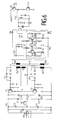
- FIG. 1 shows an inverter with the mains rectifier NG, the charging capacitor CL, the voltage divider capacitors C3, C4, the coil SP for an inductive hotplate, the capacitors C1, C2 used to limit the voltage peaks and for current transfer, and the freewheeling diodes D1 used for current transfer.
- D2 the power transistors T1, T2, the transformer Tr with the primary winding P through which the current of the transistors T1, T2 flows, the windings SbT1 and SbT2 serving to control the base, and the two secondary windings SR1 and SR2.
- the field effect transistor T13 serving as an electronic switch is connected to the ends of the windings SR1 and SR2 via the diodes D3, D4, the Zener diode Z1 being parallel to the switching path of T13.
- the rectifier circuits E1 and E2 each generate bias voltages on the capacitor by rectifying the AC voltage on the windings SbT1 and SbT2 in the sense of blocking the transistors T1 and T2. These bias voltages serve to improve the blocking and clearing of the transistors T1, T2.
- the circuit is controlled by the voltage UG at the gate of transistor T13. This voltage can be obtained with a pulse shaper from the AC output voltage of the inverter at point a. Then the circuit is self-oscillating.
- the voltage UG can also come from a separate generator.
- the current which alternately flows through the transistors T1, T2, flows in each case as current iP through the primary winding P.
- currents are induced in the windings SbT1 and SbT2, which alternately control and block the transistors T1, T2.
- the circuit of an inverter described so far is known and described in more detail in DE-PS 34 00 671 and 35 08 289.
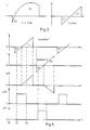
- FIG. 2 shows the curve of the voltage Ua, which represents the DC voltage for the series circuit T1, T2, and the current ia according to FIG. 1. It can be seen that the voltage Ua with a frequency of 100 Hz is not a pure DC voltage, but rather one is pulsating DC voltage, which drops periodically to zero. As already explained, this drop in amplitude affects the stable mode of operation of the inverter.
- the hatching in FIG. 2 indicates that there is a large number of switchovers between the transistors T1 and T2 during the period of 10 ms in the voltage Ua, since the working frequency of the inverter, at about 30 kHz, is substantially higher than the mains frequency.
- FIG. 3 shows the current profile in each case via D1 and T1.
- this current profile is shown for a frequency f that is slightly above the resonance frequency fres of the circuit according to FIG. 1.
- This current distribution is another reason for the unstable operation of the inverter.
- Fig. 3 shows the current curve as it appears after switching off one of the two branches in the other branch.
- the diode D1 first becomes conductive and accepts a current that drops to zero, changes its direction and is then taken over by the winding P and T1 until T1 is also switched off and the process shown is then repeated in the other branch for T2.
- UR1 is the voltage on the feedback winding SR1.
- UG is the control voltage at the gate of transistor T13.
- transistor T13 is fully conductive due to voltage UG, winding SR1 is short-circuited, and all voltages and currents at transformer TR1 are practically zero.
- the feedback from winding P to the other windings is interrupted during this time.
- the transistor T13 is blocked at time t2, the feedback path is released again.
- initially there is only a slow increase in the base current of the transistor T1 as the first part A of the rising edge of the voltage UR1 shows. This increase is initially undesirably slow.
- the rising edge A in the voltage UR1 is sufficient to control the transistor T6 so that a negatively directed pulse occurs at its collector.
- This pulse passes through the pulse shaper IF with the capacitor Ch to the base of the transistor T5, so that it is controlled to be conductive.
- the transistor T5 then generates a current pulse icT5 with the duration th from t3 - t4.
- This current flows through the winding SR1, so that the rising edge of the voltage UR1 after the flat course A now assumes the same high slope as the rising edge of the current icT5.
- the initially weak is induced Pulse is a strong pulse which is transmitted from the secondary winding SR1 to the winding SbT1 and which drives the base of the transistor T1 in such a way that this transistor is controlled to conduct in the desired manner.
- the duration of the current pulse icT5 is longer than the time period shown in FIG. 3 during which the diode D1 is conductive, since this time must be bridged by the pulse icT5.
- the base control of the transistor T1 is thus supported by the current pulse icT5 artificially fed in by T5 in the sense that the transistor T1 is controlled perfectly conductive even at low values of the voltage Ua and at all operating frequencies of the illustrated inverter.
- the circuit with T7 and T8 on the winding SR2 works in the same way in push-pull.
- the period of operation of the inverter from t1 - t7 is between 30 ⁇ s and 50 ⁇ s depending on the working frequency.
- the transistor T13 is conductive from t1-t2, t5-t6 and t7-t8, respectively, and short-circuits the windings SR1 and SR2 and thus the entire transformer Tr.
- the duration th of the current pulses through the transistors T5 and T7 is approximately 15 microseconds.
- the current iP of the transistor T1 flowing via the winding P generates the base current for the transistor T1 necessary for switching through the feedback to the winding SbT1.
- the transistor T13 then becomes conductive again at time t5 and the feedback is interrupted until the process begins again at time t6.
- the energy then still present in the transformer Tr has the result that, despite the blocking of the primary winding P, a small current can still flow into the relevant secondary winding SbT1 or SbT2, which required one in the windings SR1 and SR2 for detection by the transistors T6 and T8 Creates tension.
- 5 shows the relationship between the currents in the switch 1, formed by D1 and T1, and in the switch 2, formed by D2 and T2.
- 5 shows the components through which the current i flowing into the coil SP flows. Between T1 and D2 and T2 and D1, the current flows briefly through the capacitors C1 and C2, so that a continuous current i flows in the coil SP. The zero crossing of this current i is in each case at the transition of the current from D1 to T1 and from D2 to T2.
- the current iP is the current through the primary winding P, which corresponds to either the current through T1 or the current through T2.
- the current pulses icT5 corresponding to FIG. 4 and additionally the current pulses icT7 of the transistor T7 are shown.
- the oscillator SO is also provided, which oscillates at a frequency of 50 kHz.
- the output voltage of the oscillator SO reaches the base of T7 via the transistor T9 and from there to the winding SR2.
- the frequency of the oscillator SO is higher than the resonance frequency and causes a pulse transmission from the winding SR2 to the winding SbT2 and thus the transistor T2.
- This charges the diodes of the rectifier circuits E1 and E2 at the bases of T1 and T1.
- a voltage arises at the windings SbT1 and SbT2, which initially corresponds to the envelope of the pulse voltage at the transformer.
- a state is then reached in which one of the transistors T1 or T2 becomes conductive and the entire circuit oscillates.
- the diode DC With the diode DC, a positive voltage is obtained on the filter element RC, which controls the transistor T10 in a conductive manner and thus grounds the point d and blocks the transistor T9.
- the supply of the voltage of the oscillator SO to the circuit is interrupted.
- the circuit is then in the steady state, in which the oscillator SO is not more is needed.
- the circuit is designed to be self-oscillating in that the output a of the circuit is connected to the gate of the transistor T13 via a pulse shaper and supplies the feedback voltage UG for the transistor T13 which is used to generate vibrations.
- the transistors T6, T8 are controlled on the one hand and the current is fed into the transformer Tr via the transistors T5, T7 on the other hand by means of the same winding SR1 or SR2.
- separate windings can also be provided for these two functions.
- Each of the windings SR1 and SR2 would then consist of two separate windings, one of which controls the transistors T6, T8 and the other of which is fed by the transistors T5, T7 with the currents icT5 and icT7.
- transistors T5, T7 that is to say the circuit with the components SO, T6, T8, T9, T10, T13 and the associated passive components, is preferably designed as an integrated circuit.
- This circuit is preferably designed together with the rest of the control circuit for the transistors T1, T2 as an integrated circuit.
- This control circuit is the circuit, not shown in FIG. 1, between the output a of the inverter and the control electrode of T13, by means of which the inverter is designed to oscillate.
- Such a control circuit with additional measures to protect the inverter against overload is described in more detail in DE-PS 34 00 671 and 35 08 289.
Landscapes
- Engineering & Computer Science (AREA)
- Power Engineering (AREA)
- Physics & Mathematics (AREA)
- Electromagnetism (AREA)
- Inverter Devices (AREA)
- Circuit Arrangements For Discharge Lamps (AREA)
- Cookers (AREA)
- General Induction Heating (AREA)
Priority Applications (1)
| Application Number | Priority Date | Filing Date | Title |
|---|---|---|---|
| AT88104049T ATE97273T1 (de) | 1987-03-20 | 1988-03-15 | Wechselrichter zur speisung eines verbrauchers mit einer induktiven komponente. |
Applications Claiming Priority (4)
| Application Number | Priority Date | Filing Date | Title |
|---|---|---|---|
| DE3709250 | 1987-03-20 | ||
| DE19873709250 DE3709250A1 (de) | 1987-03-20 | 1987-03-20 | Wechselrichter zur speisung eines verbrauchers mit einer induktiven komponente |
| DE3724043 | 1987-07-21 | ||
| DE3724043A DE3724043C2 (de) | 1987-03-20 | 1987-07-21 | Wechselrichter zur Speisung eines Verbrauchers mit einer induktiven Komponente |
Publications (3)
| Publication Number | Publication Date |
|---|---|
| EP0282961A2 true EP0282961A2 (fr) | 1988-09-21 |
| EP0282961A3 EP0282961A3 (en) | 1990-05-09 |
| EP0282961B1 EP0282961B1 (fr) | 1993-11-10 |
Family
ID=25853743
Family Applications (1)
| Application Number | Title | Priority Date | Filing Date |
|---|---|---|---|
| EP88104049A Expired - Lifetime EP0282961B1 (fr) | 1987-03-20 | 1988-03-15 | Onduleur pour alimenter une charge avec composante inductive |
Country Status (5)
| Country | Link |
|---|---|
| US (1) | US4847746A (fr) |
| EP (1) | EP0282961B1 (fr) |
| KR (1) | KR960016078B1 (fr) |
| DE (2) | DE3724043C2 (fr) |
| ES (1) | ES2046994T3 (fr) |
Families Citing this family (13)
| Publication number | Priority date | Publication date | Assignee | Title |
|---|---|---|---|---|
| US5343023A (en) * | 1991-08-23 | 1994-08-30 | Miller Electric Mfg. Co. | Induction heater having a power inverter and a variable frequency output inverter |
| GB2265505B (en) * | 1992-03-19 | 1995-10-11 | Chen Su Min | Dual push-pull induction heating drive circuit |
| EP0666703A1 (fr) * | 1994-02-08 | 1995-08-09 | HUANG, Wen-Liang | Circuit de commande pour transistor de puissance pour appareil de chauffage par induction |
| BR9701473A (pt) * | 1996-04-22 | 1998-09-08 | Illinois Tool Works | Sistema e método para o aquecimento indutivo de uma peça de trabalho e sistema para a aquecimento indutivo segmentado contínuo de uma peça de trabalho |
| GB2319907A (en) * | 1996-12-02 | 1998-06-03 | Thomson Multimedia Sa | Dc-dc converter with protection circuit |
| US6163019A (en) * | 1999-03-05 | 2000-12-19 | Abb Metallurgy | Resonant frequency induction furnace system using capacitive voltage division |
| ATE349879T1 (de) | 1999-11-03 | 2007-01-15 | Nexicor Llc | Induktionshandgerät |
| RU2271595C2 (ru) * | 2000-03-29 | 2006-03-10 | Энертек Корея Ко., Лтд | Магнитная цепь с переключением |
| WO2008055545A1 (fr) * | 2006-11-09 | 2008-05-15 | Osram Gesellschaft mit beschränkter Haftung | Convertisseur cc/cc autohétérodyne et procédé à cet effet |
| ATE520279T1 (de) | 2008-12-22 | 2011-08-15 | Fagorbrandt Sas | Verfahren zur stromversorgung mit der leistung von zwei induktoren und kochgerät, bei dem dieses verfahren umgesetzt ist |
| CN103427682A (zh) * | 2013-08-14 | 2013-12-04 | 西安睿诺新能源有限公司 | 一种高性能航空电源 |
| CN108024403B (zh) * | 2016-11-03 | 2021-03-19 | 佛山市顺德区美的电热电器制造有限公司 | 电磁加热系统及其的控制方法和装置 |
| EP3721678B1 (fr) * | 2017-12-04 | 2024-01-24 | CFT S.p.A. | Dispositif de chauffage ohmique et son procédé de fonctionnement |
Family Cites Families (13)
| Publication number | Priority date | Publication date | Assignee | Title |
|---|---|---|---|---|
| US3683208A (en) * | 1970-12-23 | 1972-08-08 | North Electric Co | Power supply circuit arrangement utilizing regenerative current feedback |
| US3889090A (en) * | 1973-06-15 | 1975-06-10 | Westinghouse Electric Corp | Induction heat cooking apparatus |
| GB1507872A (en) * | 1975-02-21 | 1978-04-19 | Roband Electronics Ltd | Apparatus for generating alternating currents of accurately predetermined waveform |
| JPS51149530A (en) * | 1975-06-14 | 1976-12-22 | Sony Corp | Starting circuit for an inverter |
| GB2034541B (en) * | 1978-11-01 | 1982-12-15 | Gould Advance Ltd | Controlled power supply apparatus |
| US4319316A (en) * | 1979-10-31 | 1982-03-09 | Gould Advance Limited | Controlled power supply apparatus |
| US4301498A (en) * | 1979-10-31 | 1981-11-17 | Gould Advance Limited | Voltage converter apparatus having output regulating means |
| US4390769A (en) * | 1980-05-29 | 1983-06-28 | General Electric Company | Induction heating apparatus providing smooth power control |
| FR2578697B2 (fr) * | 1984-01-11 | 1989-04-07 | Thomson Brandt Gmbh | Convertisseur continu/alternatif pour l'alimentation d'un organe utilisateur avec une composante inductive |
| DE3508289C1 (de) * | 1985-03-08 | 1986-09-11 | Thomson Brandt Gmbh | Wechselrichter zur Speisung eines Verbrauchers mit einer induktiven Komponente |
| DE3400671C1 (de) * | 1984-01-11 | 1985-10-24 | Thomson Brandt Gmbh | Wechselrichter zur Speisung eines Verbrauchers mit einer induktiven Komponente |
| US4885447A (en) * | 1985-01-23 | 1989-12-05 | Balay, S.A. | System for the induction heating of the electric plates of a cooker |
| DE3709250A1 (de) * | 1987-03-20 | 1988-10-06 | Thomson Brandt Gmbh | Wechselrichter zur speisung eines verbrauchers mit einer induktiven komponente |
-
1987
- 1987-07-21 DE DE3724043A patent/DE3724043C2/de not_active Expired - Fee Related
-
1988
- 1988-03-15 EP EP88104049A patent/EP0282961B1/fr not_active Expired - Lifetime
- 1988-03-15 ES ES88104049T patent/ES2046994T3/es not_active Expired - Lifetime
- 1988-03-15 DE DE88104049T patent/DE3885486D1/de not_active Expired - Fee Related
- 1988-03-19 KR KR1019880002991A patent/KR960016078B1/ko not_active Expired - Lifetime
- 1988-03-21 US US07/171,178 patent/US4847746A/en not_active Expired - Fee Related
Also Published As
| Publication number | Publication date |
|---|---|
| DE3885486D1 (de) | 1993-12-16 |
| KR880011988A (ko) | 1988-10-31 |
| US4847746A (en) | 1989-07-11 |
| KR960016078B1 (ko) | 1996-11-27 |
| DE3724043A1 (de) | 1989-02-02 |
| EP0282961A3 (en) | 1990-05-09 |
| EP0282961B1 (fr) | 1993-11-10 |
| DE3724043C2 (de) | 1996-10-17 |
| ES2046994T3 (es) | 1994-02-16 |
Similar Documents
| Publication | Publication Date | Title |
|---|---|---|
| DE3319739C2 (de) | Vorschaltgerät für Gasentladungslampen | |
| EP0382110B1 (fr) | Circuit de commande de sortie pour inverseur, ainsi que source de courant haute fréquence pour l'alimentation en courant continue d'une station de sondage | |
| EP0884830B1 (fr) | Unité d'alimentation de puissance avec un onduleur modulé en largeur d'impulsion, en particulier pour un générateur de rayons X | |
| EP0282961B1 (fr) | Onduleur pour alimenter une charge avec composante inductive | |
| DE69210940T2 (de) | Leistungsumrichter | |
| EP0654886A1 (fr) | Circuit pour la génération d'une tension continue | |
| DE102012107122A1 (de) | Wechselrichterschaltung | |
| EP0203571B1 (fr) | Onduleur statique avec surélévation de courant en cas de court-circuit | |
| DE3508289C1 (de) | Wechselrichter zur Speisung eines Verbrauchers mit einer induktiven Komponente | |
| DE3400671C1 (de) | Wechselrichter zur Speisung eines Verbrauchers mit einer induktiven Komponente | |
| DE10238606A1 (de) | Schaltnetzteil | |
| DE3606462A1 (de) | Wechselrichter mit einem gleichspannungsteil und einem zerhackerteil | |
| EP0099596A1 (fr) | Circuit d'alimentation en courant électrique | |
| DE2647146A1 (de) | Spannungsregler | |
| DE3523622C2 (fr) | ||
| DE4008652A1 (de) | Netzteil mit gleichstrom-gleichstrom-wandler | |
| EP0474060B1 (fr) | Convertisseur de courant alternatif à quatre quadrants | |
| DE3709250A1 (de) | Wechselrichter zur speisung eines verbrauchers mit einer induktiven komponente | |
| DE2836610A1 (de) | Induktions-heizgeraet mit einem wechselrichter, wobei die induktionsspule des schwingkreises die heizspule fuer das kochgeschirr ist | |
| DE2819225C2 (fr) | ||
| DE2248938A1 (de) | Gleichrichter-schaltungsanordnung | |
| AT390532B (de) | Pulsbreiten moduliertes wechselstrom-leistungsstellglied | |
| EP0552389B1 (fr) | Procédé pour alimenter en énergie un électro-filtre | |
| DE3517297C1 (de) | Vorschaltgerät für Entladungslampen | |
| DE1957103C2 (de) | Umformer zur Erzeugung eines Wechselstroms aus einer Gleichspannungsquelle |
Legal Events
| Date | Code | Title | Description |
|---|---|---|---|
| PUAI | Public reference made under article 153(3) epc to a published international application that has entered the european phase |
Free format text: ORIGINAL CODE: 0009012 |
|
| AK | Designated contracting states |
Kind code of ref document: A2 Designated state(s): AT BE CH DE ES FR GB GR IT LI LU NL SE |
|
| RAP1 | Party data changed (applicant data changed or rights of an application transferred) |
Owner name: THOMSON ELECTROMENAGER S.A. |
|
| PUAL | Search report despatched |
Free format text: ORIGINAL CODE: 0009013 |
|
| AK | Designated contracting states |
Kind code of ref document: A3 Designated state(s): AT BE CH DE ES FR GB GR IT LI LU NL SE |
|
| RHK1 | Main classification (correction) |
Ipc: H02M 7/5383 |
|
| 17P | Request for examination filed |
Effective date: 19901011 |
|
| 17Q | First examination report despatched |
Effective date: 19920306 |
|
| GRAA | (expected) grant |
Free format text: ORIGINAL CODE: 0009210 |
|
| ITF | It: translation for a ep patent filed | ||
| AK | Designated contracting states |
Kind code of ref document: B1 Designated state(s): AT BE CH DE ES FR GB GR IT LI LU NL SE |
|
| REF | Corresponds to: |
Ref document number: 97273 Country of ref document: AT Date of ref document: 19931115 Kind code of ref document: T |
|
| GBT | Gb: translation of ep patent filed (gb section 77(6)(a)/1977) |
Effective date: 19931112 |
|
| REF | Corresponds to: |
Ref document number: 3885486 Country of ref document: DE Date of ref document: 19931216 |
|
| BECA | Be: change of holder's address |
Free format text: 931110 S.A. *THOMSON ELECTROMENAGER:122 AVENUE DU GENERAL LECLERC, F-92100 BOULOGNE-BILLANCOURT |
|
| REG | Reference to a national code |
Ref country code: GR Ref legal event code: FG4A Free format text: 3009897 |
|
| REG | Reference to a national code |
Ref country code: ES Ref legal event code: FG2A Ref document number: 2046994 Country of ref document: ES Kind code of ref document: T3 |
|
| ET | Fr: translation filed | ||
| PGFP | Annual fee paid to national office [announced via postgrant information from national office to epo] |
Ref country code: GR Payment date: 19940324 Year of fee payment: 7 |
|
| PG25 | Lapsed in a contracting state [announced via postgrant information from national office to epo] |
Ref country code: LU Free format text: LAPSE BECAUSE OF NON-PAYMENT OF DUE FEES Effective date: 19940331 Ref country code: LI Effective date: 19940331 Ref country code: CH Effective date: 19940331 |
|
| PLBE | No opposition filed within time limit |
Free format text: ORIGINAL CODE: 0009261 |
|
| STAA | Information on the status of an ep patent application or granted ep patent |
Free format text: STATUS: NO OPPOSITION FILED WITHIN TIME LIMIT |
|
| 26N | No opposition filed | ||
| REG | Reference to a national code |
Ref country code: CH Ref legal event code: AUV Free format text: DAS OBENGENANNTE PATENT, IST MANGELS BEZAHLUNG DER 7. JAHRESGEBUEHR, GELOESCHT WORDEN. Ref country code: CH Ref legal event code: PL |
|
| EAL | Se: european patent in force in sweden |
Ref document number: 88104049.7 |
|
| PGFP | Annual fee paid to national office [announced via postgrant information from national office to epo] |
Ref country code: SE Payment date: 19950217 Year of fee payment: 8 |
|
| PGFP | Annual fee paid to national office [announced via postgrant information from national office to epo] |
Ref country code: GB Payment date: 19950220 Year of fee payment: 8 |
|
| PGFP | Annual fee paid to national office [announced via postgrant information from national office to epo] |
Ref country code: BE Payment date: 19950306 Year of fee payment: 8 |
|
| PGFP | Annual fee paid to national office [announced via postgrant information from national office to epo] |
Ref country code: AT Payment date: 19950309 Year of fee payment: 8 |
|
| PGFP | Annual fee paid to national office [announced via postgrant information from national office to epo] |
Ref country code: ES Payment date: 19950315 Year of fee payment: 8 |
|
| PGFP | Annual fee paid to national office [announced via postgrant information from national office to epo] |
Ref country code: NL Payment date: 19950331 Year of fee payment: 8 |
|
| PG25 | Lapsed in a contracting state [announced via postgrant information from national office to epo] |
Ref country code: GR Free format text: THE PATENT HAS BEEN ANNULLED BY A DECISION OF A NATIONAL AUTHORITY Effective date: 19950930 |
|
| REG | Reference to a national code |
Ref country code: GR Ref legal event code: MM2A Free format text: 3009897 |
|
| PG25 | Lapsed in a contracting state [announced via postgrant information from national office to epo] |
Ref country code: GB Effective date: 19960315 Ref country code: AT Effective date: 19960315 |
|
| PG25 | Lapsed in a contracting state [announced via postgrant information from national office to epo] |
Ref country code: SE Effective date: 19960316 Ref country code: ES Free format text: LAPSE BECAUSE OF NON-PAYMENT OF DUE FEES Effective date: 19960316 |
|
| PG25 | Lapsed in a contracting state [announced via postgrant information from national office to epo] |
Ref country code: BE Effective date: 19960331 |
|
| BERE | Be: lapsed |
Owner name: S.A. THOMSON ELECTROMENAGER Effective date: 19960331 |
|
| PG25 | Lapsed in a contracting state [announced via postgrant information from national office to epo] |
Ref country code: NL Effective date: 19961001 |
|
| GBPC | Gb: european patent ceased through non-payment of renewal fee |
Effective date: 19960315 |
|
| NLV4 | Nl: lapsed or anulled due to non-payment of the annual fee |
Effective date: 19961001 |
|
| EUG | Se: european patent has lapsed |
Ref document number: 88104049.7 |
|
| REG | Reference to a national code |
Ref country code: ES Ref legal event code: FD2A Effective date: 19990405 |
|
| PGFP | Annual fee paid to national office [announced via postgrant information from national office to epo] |
Ref country code: FR Payment date: 20030307 Year of fee payment: 16 |
|
| PGFP | Annual fee paid to national office [announced via postgrant information from national office to epo] |
Ref country code: DE Payment date: 20030526 Year of fee payment: 16 |
|
| PG25 | Lapsed in a contracting state [announced via postgrant information from national office to epo] |
Ref country code: DE Free format text: LAPSE BECAUSE OF NON-PAYMENT OF DUE FEES Effective date: 20041001 |
|
| PG25 | Lapsed in a contracting state [announced via postgrant information from national office to epo] |
Ref country code: FR Free format text: LAPSE BECAUSE OF NON-PAYMENT OF DUE FEES Effective date: 20041130 |
|
| REG | Reference to a national code |
Ref country code: FR Ref legal event code: ST |
|
| PG25 | Lapsed in a contracting state [announced via postgrant information from national office to epo] |
Ref country code: IT Free format text: LAPSE BECAUSE OF NON-PAYMENT OF DUE FEES;WARNING: LAPSES OF ITALIAN PATENTS WITH EFFECTIVE DATE BEFORE 2007 MAY HAVE OCCURRED AT ANY TIME BEFORE 2007. THE CORRECT EFFECTIVE DATE MAY BE DIFFERENT FROM THE ONE RECORDED. Effective date: 20050315 |