EP0283276A2 - Halbleiteranordnung mit einem Hetero-Übergang und Verfahren zu deren Herstellung - Google Patents
Halbleiteranordnung mit einem Hetero-Übergang und Verfahren zu deren Herstellung Download PDFInfo
- Publication number
- EP0283276A2 EP0283276A2 EP88302312A EP88302312A EP0283276A2 EP 0283276 A2 EP0283276 A2 EP 0283276A2 EP 88302312 A EP88302312 A EP 88302312A EP 88302312 A EP88302312 A EP 88302312A EP 0283276 A2 EP0283276 A2 EP 0283276A2
- Authority
- EP
- European Patent Office
- Prior art keywords
- semiconductor layer
- heterojunction
- set forth
- undoped
- electrodes
- Prior art date
- Legal status (The legal status is an assumption and is not a legal conclusion. Google has not performed a legal analysis and makes no representation as to the accuracy of the status listed.)
- Withdrawn
Links
Images



Classifications
-
- B—PERFORMING OPERATIONS; TRANSPORTING
- B82—NANOTECHNOLOGY
- B82Y—SPECIFIC USES OR APPLICATIONS OF NANOSTRUCTURES; MEASUREMENT OR ANALYSIS OF NANOSTRUCTURES; MANUFACTURE OR TREATMENT OF NANOSTRUCTURES
- B82Y10/00—Nanotechnology for information processing, storage or transmission, e.g. quantum computing or single electron logic
-
- H—ELECTRICITY
- H10—SEMICONDUCTOR DEVICES; ELECTRIC SOLID-STATE DEVICES NOT OTHERWISE PROVIDED FOR
- H10D—INORGANIC ELECTRIC SEMICONDUCTOR DEVICES
- H10D30/00—Field-effect transistors [FET]
- H10D30/40—FETs having zero-dimensional [0D], one-dimensional [1D] or two-dimensional [2D] charge carrier gas channels
- H10D30/43—FETs having zero-dimensional [0D], one-dimensional [1D] or two-dimensional [2D] charge carrier gas channels having one-dimensional [1D] charge carrier gas channels, e.g. quantum wire FETs or transistors having 1D quantum-confined channels
-
- H—ELECTRICITY
- H10—SEMICONDUCTOR DEVICES; ELECTRIC SOLID-STATE DEVICES NOT OTHERWISE PROVIDED FOR
- H10D—INORGANIC ELECTRIC SEMICONDUCTOR DEVICES
- H10D64/00—Electrodes of devices having potential barriers
- H10D64/20—Electrodes characterised by their shapes, relative sizes or dispositions
- H10D64/27—Electrodes not carrying the current to be rectified, amplified, oscillated or switched, e.g. gates
- H10D64/311—Gate electrodes for field-effect devices
- H10D64/411—Gate electrodes for field-effect devices for FETs
Definitions
- the present invention relates to a semiconductor device and a method for producing the device. More particularly, it relates to a structure of a transistor having a heterojunction.
- a high electron mobility transistor As a semiconductor device having a heterojunction structure, a high electron mobility transistor (HEMT) is widely known.
- the HEMT includes a structure wherein an undoped semiconductor layer and a doped semiconductor layer are in contact with each other, and at the interface of these semiconductor layers, electrons are accumulated to form a kind of layer defined as a two-dimensional electron layer or gas (2 DEG).
- 2 DEG two-dimensional electron layer or gas
- electrons travel within the 2 DEG from a source toward a drain without being scattered by impurity ions, and as a result, a very high electron mobility can be obtained.
- the movement of electrons is realized in a two-dimensional direction.
- the structure wherein the movement of electrons occurred in a one-dimensional direction is desired.
- a device using a one-dimensional electron layer or gas (1 DEG) would show a higher operation speed than that using a 2 DEG, and such a device is disclosed, for example, in p.p. 251 - 256, of a Paper presented at the Int. Symp., GaAs and Related Compounds, Japan, 1981.
- the device disclosed in the above Paper has a metal/insulation/semiconductor (MIS) structure and employs gallium arsenide (GaAs) as the semiconductor.
- MIS metal/insulation/semiconductor
- GaAs gallium arsenide
- a PBT includes a structure wherein a fine slit-shaped metal grid is embedded in a layer of a single crystal such as GaAs and the flow of carriers passing through gaps of the metal grid is controlled by applying a controlled voltage to the metal grid.
- a PBT is disclosed, for example, in U.S.P. 4,378,629, wherein carriers travel from an emitter toward a collector in a "vertical" direction. This kind of PBT is hereinafter referred to as a "vertical type or structure" PBT.
- Such a PBT includes a structure wherein a fine metal grid is embedded in the vertical direction in a single-crystalline layer and carriers travel through gaps of the metal grid in the "horizontal" direction.
- the structure of the horizontal type PBT makes it possible to prevent the surface of the semiconductor from being contaminated by impurities in the course of the production process, and thus the above problem of the vertical type PBT can be solved. Nevertheless, if possible, a device realizing a much higher speed operation is desired.
- a device having a structure similar to that of the horizontal type PBT is disclosed, for example, in Japanese Unexamined Patent Publication (Kokai) No. 62-2666.
- An embodiment of the present invention may provide a semiconductor device capable of realizing a higher speed operation without lowering the controllability thereof as a transistor.
- An embodiment of the present invention may provide a method for producing the device.
- the present invention utilises the idea of combining the structure of an HEMT and the structure of a "horizontal type" PBT.
- a semiconductor device comprising: a heterojunction semiconductor layer formed on a substrate, having a structure including an undoped semiconductor layer sandwiched between two doped semiconductor layers; two electrodes formed opposite to each other on the heterojunction semiconductor layer; and a plurality of control electrodes arranged at predetermined positions between the two electrodes at a predetermined spacing, a portion of each control electrode being embedded in such a manner that the portion is in direct contact with a section of the heterojunction semiconductor layer, whereby the direction of the movement of carriers within the undoped semiconductor layer is made one-dimensional in the vicinity of the control electrodes.
- a method for producing a semiconductor device comprising the steps of: growing a heterojunction semiconductor layer on a substrate,said heterojunction semiconductor layer comprising a structure including an undoped semiconductor layer sandwiched between doped semiconductor layers; forming two electrodes opposite to each other on the heterojunction semiconductor layer; and embedding a plurality of control electrodes at predetermined positions between the two electrodes at a predetermined spacing in such a manner that a portion of each control electrode is in direct contact with a section of the heterojunction semiconductor layer, whereby the direction of the movement of carriers is made one-dimensional in the vicinity of the control electrodes.
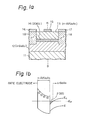
- Figures 1a and 1b show an example of a typical HEMT; wherein Fig. 1a shows a section thereof and Fig. 1b shows an energy band taken along the line B-B in Fig. 1a.
- 11 denotes a substrate
- 12 and 13 denote semiconductor layers
- 14 denotes a two-dimensional electron layer or gas (2 DEG)
- 15, 16, and 17 denote electrodes
- 18 denotes an alloyed region.
- an HEMT is characterized in that semiconductor layers 12 and 13 are in heterocontact with each other, and that only one thereof, i.e., semiconductor layer 13 in the illustrated example, is selectively doped to form an n-type layer.
- This HEMT structure can realize a very high electron mobility, because impurity atoms or ions are not introduced into the semiconductor layer 12 of i-GaAs and, accordingly, electrons within the 2 DEG travel along the interface in the side of the semiconductor layer 12 from the source electrode 16 toward the drain electrode 17 without being scattered by the impurity atoms or ions.
- the movement of electrons is realized along a plane parallel to the 2 DEG 14, i.e., in a two-dimensional direction.
- a device using a 1 DEG would show a higher operation speed than that using a 2 DEG.
- an FET employing an inversion layer as the 1 DEG is shown in Fig. 2.
- 21 and 23 denote semiconductor layers of p-AlGaAs; 22 denotes a semiconductor layer of p-GaAs; 24 denotes an insulation layer; 25 denotes a metal layer constituting a gate; and 26 denotes an n-type inversion layer constituting 1 DEG.
- the FET shown in Fig. 2 has an MIS structure and employs GaAs as the semiconductor, and thus does not constitute a good MISFET from the viewpoint of gate controllability, as hereinafter described.
- the GaAs layer 22 and AlGaAs layers 21 and 23 are etched into a V-shape, and the etching is carried out by utilizing the dependency of a face orientation of a GaAs wafer with respect to wet etching.
- the controllability of the etching is not good or not practical.
- Figure 3 illustrates an example of a vertical type PBT, in perspective, with portions broken away for clarity.
- 31 and 33 denote semiconductor layers of n-GaAs; 35 denotes a collector electrode; 34 denotes an insulation layer; 32 denotes an emitter electrode; 36 denotes a base electrode embedded in a crystalline growth layer; and 37 denotes a common electrode for connecting the base electrode 36 to the external.
- 31 and 33 denote semiconductor layers of n-GaAs
- 35 denotes a collector electrode
- 34 denotes an insulation layer
- 32 denotes an emitter electrode
- 36 denotes a base electrode embedded in a crystalline growth layer
- 37 denotes a common electrode for connecting the base electrode 36 to the external.
- the production process of the vertical type PBT as shown in Fig. 3 must include the following steps; first, growing the semiconductor layers 31 and 33 halfway in the vacuum state; second, taking the grown semiconductor layers out of the vacuum atmosphere, i.e., placing in the open atmosphere, and carrying out ion implantation for forming the insulation layer 34, patterning for forming the base electrode 36 and common electrode 37, metal deposition, and the like; third, growing the remaining portions of the semiconductor layers again in the vacuum state.
- Figure 4 illustrates a permeable base high electron mobility transistor (PB-HEMT) as an embodiment of the present invention, in perspective, with portions broken away for clarity.
- 41 denotes a semiinsulation substrate of GaAs
- 42 denotes a heterojunction semiconductor layer grown on the substrate 41 and having a structure wherein an undoped semiconductor layer 42C of i-GaAs having a thickness of less than 100 ⁇ (10 nm) is sandwiched between two doped semiconductor layers 42A and 42B of n-AlGaAs.
- the electron affinity is lower in the doped semiconductor layers 42A and 42B than in the undoped semiconductor layer 42C. Otherwise, the sum of the electron affinity and an energy gap is greater in the doped layers than in the undoped layer.
- Reference 43 denotes an emitter electrode
- 44 denotes a collector electrode
- reference 45 denotes one of a plurality of base electrodes.
- Base electrodes 45 are arranged midway between the emitter and collector electrodes, at a predetermined spacing, e.g., 1000 ⁇ or less in the present example, and along the direction perpendicular to the direction of movement from the emitter electrode to the collector electrode. A portion of each base electrode 45 is embedded in the heterojunction semiconductor layer 42.
- Reference 46 denotes an insulation layer for insulating the electrodes
- reference 47 denotes a common base electrode, which electrically interconnects the plurality of base electrodes 45 to keep them at an equal potential and, accordingly, reduces the base resistance as a transistor.
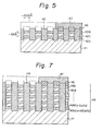
- Figure 5 shows a section taken along the line A-A in Fig. 4.
- the thickness of the intrinsic semiconductor layer 42C is very small (100 ⁇ (10 nm) or less), and the length in the direction of the width of the laye 42C is separated into small widths of less than 1000 ⁇ (100 nm) by the base electrodes 45 having a comb-like shape.
- the intrinsic semiconductor layer 42C constitutes channels defined as a one-dimensional direction, i.e., a one-dimensional electron layer or gas (1 DEG). Electrons move through the channels from the emitter electrode 43 (not shown in Fig. 5) to the collector electrode 44 (not shown in Fig. 5).
- a higher electron mobility can be realized, because the direction of movement of the electrons is one-dimensional in the vicinity of the base electrodes 45. Also, since each of the base electrodes 45 is in direct contact with the heterojunction semiconductor layer 42, the controllability as a transistor can be improved.
- the present device constitutes a PBT having a "horizontal type” structure
- the advantage as hereinafter described is obtained. Namely, according to the production process of the device shown in Fig. 4, which will be explained later in detail, it is not necessary to expose the semiconductor layers to an open atmosphere during the process of growing the semiconductor layers in the vacuum atmosphere, and as a result, it is possible to solve the problem occurring in the "vertical type" PBT of impurities remaining in the semiconductor layers due to a process such as metal deposition during the forming of the base electrode. This advantage contributes to a further acceleration of a high speed operation.
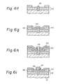
- a first step Si-doped AlGaAs is grown by molecular beam epitaxy (MBE) on the semiinsulation substrate 41 of GaAs to form the semiconductor layer 42A of n-AlGaAs.
- MBE molecular beam epitaxy
- undoped GaAs is grown by MBE to form the intrinsic semiconductor layer 42C of i-GaAs, having a thickness of 100 ⁇ (10 nm) or less. Note the thickness must be such that the movement of electrons in the vertical direction is brought to quantization.
- Si-doped AlGaAs is grown MBE to form the semiconductor layer 42B of n-AlGaAs.
- the heterojunction semiconductor layer 42 is formed on the substrate 41.
- a fourth step metal is deposited at predetermined portions on the heterojunction semiconductor layer to form the emitter electrode 43 and collector electrode 44.
- a fifth step (see Fig. 6e) patterning for the forming of the base electrodes is carried out and a resist 51 is then formed.
- dry etching is carried out to a depth reaching the substrate 41, to form a plurality of recess portions in which a corresponding plurality of base electrodes are embedded.
- the resist is removed by lift-off and the base electrodes 45 are formed.
- a seventh step SiO2 or Si3N4 is deposited to form the insulation layer 46 for insulating each electrode
- an eighth step (see Fig. 6h)
- patterning for the forming of the. common base electrode is carried out and a resist 52 is then formed.
- dry etching is carried out to a depth reaching the base electrodes 45, and in the final step (see Fig. 6i), the resist is removed by lift-off and metal is then deposited and forms the common base electrode 47.
- the device having a single 1 DEGs i.e., intrinsic semiconductor layer
- a device having a plurality of 1 DEGs may be embodied as shown in Fig. 7.
- Figure 7 illustrates a section, corresponding to the section shown in Fig. 5, of a modification of the PB-HEMT shown in Fig. 4.
- a plurality of one-dimensional electron layers (1 DEGs) are formed as a multi-layer structure.
- the heterojunction semiconductor layer 48 has a structure wherein a plurality of semiconductor layers 48A of n-AlGaAs and a plurality of semiconductor layers 48B of i-GaAs are deposited in turn so that heterojunction structures are formed.
- the intrinsic semiconductor layers 48B constitute 2 DEGs.
Landscapes
- Engineering & Computer Science (AREA)
- Chemical & Material Sciences (AREA)
- Nanotechnology (AREA)
- Physics & Mathematics (AREA)
- Mathematical Physics (AREA)
- Theoretical Computer Science (AREA)
- Crystallography & Structural Chemistry (AREA)
- Junction Field-Effect Transistors (AREA)
- Bipolar Transistors (AREA)
Applications Claiming Priority (2)
| Application Number | Priority Date | Filing Date | Title |
|---|---|---|---|
| JP62064171A JPS63232374A (ja) | 1987-03-20 | 1987-03-20 | 半導体装置 |
| JP64171/87 | 1987-03-20 |
Publications (2)
| Publication Number | Publication Date |
|---|---|
| EP0283276A2 true EP0283276A2 (de) | 1988-09-21 |
| EP0283276A3 EP0283276A3 (de) | 1988-11-09 |
Family
ID=13250348
Family Applications (1)
| Application Number | Title | Priority Date | Filing Date |
|---|---|---|---|
| EP88302312A Withdrawn EP0283276A3 (de) | 1987-03-20 | 1988-03-17 | Halbleiteranordnung mit einem Hetero-Übergang und Verfahren zu deren Herstellung |
Country Status (2)
| Country | Link |
|---|---|
| EP (1) | EP0283276A3 (de) |
| JP (1) | JPS63232374A (de) |
Cited By (4)
| Publication number | Priority date | Publication date | Assignee | Title |
|---|---|---|---|---|
| GB2259806A (en) * | 1991-09-12 | 1993-03-24 | Mitsubishi Electric Corp | Semiconductor device and method of producing it |
| FR2696583A1 (fr) * | 1992-10-06 | 1994-04-08 | Mitsubishi Electric Corp | Dispositif à semiconducteurs, à couche de canal et couche d'alimentation en électrons, et procédé de fabrication. |
| EP0370403B1 (de) * | 1988-11-19 | 1997-09-03 | Research Development Corporation Of Japan | Halbleiter mit einer Matrixstruktur aus gekoppelten Quanten-Schachteln |
| CN107195773A (zh) * | 2017-06-26 | 2017-09-22 | 中国科学技术大学 | 空穴型半导体异质结霍尔棒、其制备和使用方法及用途 |
Family Cites Families (1)
| Publication number | Priority date | Publication date | Assignee | Title |
|---|---|---|---|---|
| JPS5931071A (ja) * | 1982-08-13 | 1984-02-18 | Oki Electric Ind Co Ltd | 電界効果トランジスタ |
-
1987
- 1987-03-20 JP JP62064171A patent/JPS63232374A/ja active Pending
-
1988
- 1988-03-17 EP EP88302312A patent/EP0283276A3/de not_active Withdrawn
Cited By (7)
| Publication number | Priority date | Publication date | Assignee | Title |
|---|---|---|---|---|
| EP0370403B1 (de) * | 1988-11-19 | 1997-09-03 | Research Development Corporation Of Japan | Halbleiter mit einer Matrixstruktur aus gekoppelten Quanten-Schachteln |
| GB2259806A (en) * | 1991-09-12 | 1993-03-24 | Mitsubishi Electric Corp | Semiconductor device and method of producing it |
| US5270556A (en) * | 1991-09-12 | 1993-12-14 | Mitsubishi Denki Kabushiki Kaisha | Semiconductor device with upper and lower gate electrode structure |
| US5369044A (en) * | 1991-09-12 | 1994-11-29 | Mitsubishi Denki Kabushiki Kaisha | Method for producing a semiconductor device |
| GB2259806B (en) * | 1991-09-12 | 1995-05-31 | Mitsubishi Electric Corp | Semiconductor device and method for producing the semiconductor device |
| FR2696583A1 (fr) * | 1992-10-06 | 1994-04-08 | Mitsubishi Electric Corp | Dispositif à semiconducteurs, à couche de canal et couche d'alimentation en électrons, et procédé de fabrication. |
| CN107195773A (zh) * | 2017-06-26 | 2017-09-22 | 中国科学技术大学 | 空穴型半导体异质结霍尔棒、其制备和使用方法及用途 |
Also Published As
| Publication number | Publication date |
|---|---|
| EP0283276A3 (de) | 1988-11-09 |
| JPS63232374A (ja) | 1988-09-28 |
Similar Documents
| Publication | Publication Date | Title |
|---|---|---|
| US4683487A (en) | Heterojunction bipolar transistor | |
| EP1088346A1 (de) | Quantendraht-feldeffekttransistor und verfahren zu dessen herstellung | |
| EP0657942A2 (de) | Lateraler Bipolartransistor | |
| US5406094A (en) | Quantum interference effect semiconductor device and method of producing the same | |
| US5212404A (en) | Semiconductor device having a vertical channel of carriers | |
| EP0283276A2 (de) | Halbleiteranordnung mit einem Hetero-Übergang und Verfahren zu deren Herstellung | |
| US4785340A (en) | Semiconductor device having doping multilayer structure | |
| EP0602671B1 (de) | Heteroübergangsfeldeffekttransistor mit verbesserter Transistorseigenschaft | |
| JP2863793B2 (ja) | 半導体装置及びその製造方法 | |
| US6242765B1 (en) | Field effect transistor and its manufacturing method | |
| JPH0575139A (ja) | 半導体装置及びその製造方法 | |
| JP2626220B2 (ja) | 電界効果トランジスタ及びその製造方法 | |
| JP3075769B2 (ja) | 静電誘導トランジスタ及びその製造方法 | |
| EP0538792B1 (de) | Mehrkanal-FET mit schmaler Linienbreite und mit verbesserten Rauschcharakteristiken | |
| JP3747391B2 (ja) | 化合物半導体装置及びその製造方法 | |
| EP0276981B1 (de) | Integrierte Halbleiterschaltung und Verfahren zu deren Herstellung | |
| JP3106747B2 (ja) | 化合物半導体fetの製造方法 | |
| JPH07105473B2 (ja) | Mes fetの製造方法 | |
| GB2239557A (en) | High electron mobility transistors | |
| JPH04369843A (ja) | 半導体装置およびその製造方法 | |
| JP2541240B2 (ja) | 半導体装置 | |
| JP2836145B2 (ja) | 電界効果トランジスタおよびその製造方法 | |
| JPS63287058A (ja) | ヘテロ接合バイポ−ラトランジスタの製造方法 | |
| JP2902812B2 (ja) | 半導体装置 | |
| JPH05102198A (ja) | 擬1次元電界効果トランジスタとその製造方法 |
Legal Events
| Date | Code | Title | Description |
|---|---|---|---|
| PUAI | Public reference made under article 153(3) epc to a published international application that has entered the european phase |
Free format text: ORIGINAL CODE: 0009012 |
|
| PUAL | Search report despatched |
Free format text: ORIGINAL CODE: 0009013 |
|
| AK | Designated contracting states |
Kind code of ref document: A2 Designated state(s): DE FR GB |
|
| AK | Designated contracting states |
Kind code of ref document: A3 Designated state(s): DE FR GB |
|
| STAA | Information on the status of an ep patent application or granted ep patent |
Free format text: STATUS: THE APPLICATION IS DEEMED TO BE WITHDRAWN |
|
| 18D | Application deemed to be withdrawn |
Effective date: 19890510 |