EP0284031A2 - Opto-electronic device - Google Patents
Opto-electronic device Download PDFInfo
- Publication number
- EP0284031A2 EP0284031A2 EP88104589A EP88104589A EP0284031A2 EP 0284031 A2 EP0284031 A2 EP 0284031A2 EP 88104589 A EP88104589 A EP 88104589A EP 88104589 A EP88104589 A EP 88104589A EP 0284031 A2 EP0284031 A2 EP 0284031A2
- Authority
- EP
- European Patent Office
- Prior art keywords
- semiconductor
- opto
- layer
- electronic device
- superlattice
- Prior art date
- Legal status (The legal status is an assumption and is not a legal conclusion. Google has not performed a legal analysis and makes no representation as to the accuracy of the status listed.)
- Ceased
Links
Images

Classifications
-
- H—ELECTRICITY
- H10—SEMICONDUCTOR DEVICES; ELECTRIC SOLID-STATE DEVICES NOT OTHERWISE PROVIDED FOR
- H10H—INORGANIC LIGHT-EMITTING SEMICONDUCTOR DEVICES HAVING POTENTIAL BARRIERS
- H10H20/00—Individual inorganic light-emitting semiconductor devices having potential barriers, e.g. light-emitting diodes [LED]
- H10H20/80—Constructional details
- H10H20/81—Bodies
- H10H20/811—Bodies having quantum effect structures or superlattices, e.g. tunnel junctions
- H10H20/812—Bodies having quantum effect structures or superlattices, e.g. tunnel junctions within the light-emitting regions, e.g. having quantum confinement structures
-
- B—PERFORMING OPERATIONS; TRANSPORTING
- B82—NANOTECHNOLOGY
- B82Y—SPECIFIC USES OR APPLICATIONS OF NANOSTRUCTURES; MEASUREMENT OR ANALYSIS OF NANOSTRUCTURES; MANUFACTURE OR TREATMENT OF NANOSTRUCTURES
- B82Y20/00—Nanooptics, e.g. quantum optics or photonic crystals
-
- H—ELECTRICITY
- H01—ELECTRIC ELEMENTS
- H01S—DEVICES USING THE PROCESS OF LIGHT AMPLIFICATION BY STIMULATED EMISSION OF RADIATION [LASER] TO AMPLIFY OR GENERATE LIGHT; DEVICES USING STIMULATED EMISSION OF ELECTROMAGNETIC RADIATION IN WAVE RANGES OTHER THAN OPTICAL
- H01S5/00—Semiconductor lasers
- H01S5/30—Structure or shape of the active region; Materials used for the active region
- H01S5/32—Structure or shape of the active region; Materials used for the active region comprising PN junctions, e.g. hetero- or double- heterostructures
-
- H—ELECTRICITY
- H01—ELECTRIC ELEMENTS
- H01S—DEVICES USING THE PROCESS OF LIGHT AMPLIFICATION BY STIMULATED EMISSION OF RADIATION [LASER] TO AMPLIFY OR GENERATE LIGHT; DEVICES USING STIMULATED EMISSION OF ELECTROMAGNETIC RADIATION IN WAVE RANGES OTHER THAN OPTICAL
- H01S5/00—Semiconductor lasers
- H01S5/30—Structure or shape of the active region; Materials used for the active region
- H01S5/34—Structure or shape of the active region; Materials used for the active region comprising quantum well or superlattice structures, e.g. single quantum well [SQW] lasers, multiple quantum well [MQW] lasers or graded index separate confinement heterostructure [GRINSCH] lasers
-
- H—ELECTRICITY
- H01—ELECTRIC ELEMENTS
- H01S—DEVICES USING THE PROCESS OF LIGHT AMPLIFICATION BY STIMULATED EMISSION OF RADIATION [LASER] TO AMPLIFY OR GENERATE LIGHT; DEVICES USING STIMULATED EMISSION OF ELECTROMAGNETIC RADIATION IN WAVE RANGES OTHER THAN OPTICAL
- H01S5/00—Semiconductor lasers
- H01S5/30—Structure or shape of the active region; Materials used for the active region
- H01S5/34—Structure or shape of the active region; Materials used for the active region comprising quantum well or superlattice structures, e.g. single quantum well [SQW] lasers, multiple quantum well [MQW] lasers or graded index separate confinement heterostructure [GRINSCH] lasers
- H01S5/347—Structure or shape of the active region; Materials used for the active region comprising quantum well or superlattice structures, e.g. single quantum well [SQW] lasers, multiple quantum well [MQW] lasers or graded index separate confinement heterostructure [GRINSCH] lasers in AIIBVI compounds, e.g. ZnCdSe- laser
-
- H—ELECTRICITY
- H01—ELECTRIC ELEMENTS
- H01S—DEVICES USING THE PROCESS OF LIGHT AMPLIFICATION BY STIMULATED EMISSION OF RADIATION [LASER] TO AMPLIFY OR GENERATE LIGHT; DEVICES USING STIMULATED EMISSION OF ELECTROMAGNETIC RADIATION IN WAVE RANGES OTHER THAN OPTICAL
- H01S2302/00—Amplification / lasing wavelength
-
- H—ELECTRICITY
- H01—ELECTRIC ELEMENTS
- H01S—DEVICES USING THE PROCESS OF LIGHT AMPLIFICATION BY STIMULATED EMISSION OF RADIATION [LASER] TO AMPLIFY OR GENERATE LIGHT; DEVICES USING STIMULATED EMISSION OF ELECTROMAGNETIC RADIATION IN WAVE RANGES OTHER THAN OPTICAL
- H01S5/00—Semiconductor lasers
- H01S5/20—Structure or shape of the semiconductor body to guide the optical wave ; Confining structures perpendicular to the optical axis, e.g. index or gain guiding, stripe geometry, broad area lasers, gain tailoring, transverse or lateral reflectors, special cladding structures, MQW barrier reflection layers
- H01S5/2004—Confining in the direction perpendicular to the layer structure
-
- H—ELECTRICITY
- H01—ELECTRIC ELEMENTS
- H01S—DEVICES USING THE PROCESS OF LIGHT AMPLIFICATION BY STIMULATED EMISSION OF RADIATION [LASER] TO AMPLIFY OR GENERATE LIGHT; DEVICES USING STIMULATED EMISSION OF ELECTROMAGNETIC RADIATION IN WAVE RANGES OTHER THAN OPTICAL
- H01S5/00—Semiconductor lasers
- H01S5/20—Structure or shape of the semiconductor body to guide the optical wave ; Confining structures perpendicular to the optical axis, e.g. index or gain guiding, stripe geometry, broad area lasers, gain tailoring, transverse or lateral reflectors, special cladding structures, MQW barrier reflection layers
- H01S5/22—Structure or shape of the semiconductor body to guide the optical wave ; Confining structures perpendicular to the optical axis, e.g. index or gain guiding, stripe geometry, broad area lasers, gain tailoring, transverse or lateral reflectors, special cladding structures, MQW barrier reflection layers having a ridge or stripe structure
- H01S5/2205—Structure or shape of the semiconductor body to guide the optical wave ; Confining structures perpendicular to the optical axis, e.g. index or gain guiding, stripe geometry, broad area lasers, gain tailoring, transverse or lateral reflectors, special cladding structures, MQW barrier reflection layers having a ridge or stripe structure comprising special burying or current confinement layers
- H01S5/2214—Structure or shape of the semiconductor body to guide the optical wave ; Confining structures perpendicular to the optical axis, e.g. index or gain guiding, stripe geometry, broad area lasers, gain tailoring, transverse or lateral reflectors, special cladding structures, MQW barrier reflection layers having a ridge or stripe structure comprising special burying or current confinement layers based on oxides or nitrides
-
- H—ELECTRICITY
- H01—ELECTRIC ELEMENTS
- H01S—DEVICES USING THE PROCESS OF LIGHT AMPLIFICATION BY STIMULATED EMISSION OF RADIATION [LASER] TO AMPLIFY OR GENERATE LIGHT; DEVICES USING STIMULATED EMISSION OF ELECTROMAGNETIC RADIATION IN WAVE RANGES OTHER THAN OPTICAL
- H01S5/00—Semiconductor lasers
- H01S5/30—Structure or shape of the active region; Materials used for the active region
- H01S5/32—Structure or shape of the active region; Materials used for the active region comprising PN junctions, e.g. hetero- or double- heterostructures
- H01S5/3206—Structure or shape of the active region; Materials used for the active region comprising PN junctions, e.g. hetero- or double- heterostructures ordering or disordering the natural superlattice in ternary or quaternary materials
-
- H—ELECTRICITY
- H01—ELECTRIC ELEMENTS
- H01S—DEVICES USING THE PROCESS OF LIGHT AMPLIFICATION BY STIMULATED EMISSION OF RADIATION [LASER] TO AMPLIFY OR GENERATE LIGHT; DEVICES USING STIMULATED EMISSION OF ELECTROMAGNETIC RADIATION IN WAVE RANGES OTHER THAN OPTICAL
- H01S5/00—Semiconductor lasers
- H01S5/30—Structure or shape of the active region; Materials used for the active region
- H01S5/32—Structure or shape of the active region; Materials used for the active region comprising PN junctions, e.g. hetero- or double- heterostructures
- H01S5/3206—Structure or shape of the active region; Materials used for the active region comprising PN junctions, e.g. hetero- or double- heterostructures ordering or disordering the natural superlattice in ternary or quaternary materials
- H01S5/3207—Structure or shape of the active region; Materials used for the active region comprising PN junctions, e.g. hetero- or double- heterostructures ordering or disordering the natural superlattice in ternary or quaternary materials ordered active layer
-
- H—ELECTRICITY
- H01—ELECTRIC ELEMENTS
- H01S—DEVICES USING THE PROCESS OF LIGHT AMPLIFICATION BY STIMULATED EMISSION OF RADIATION [LASER] TO AMPLIFY OR GENERATE LIGHT; DEVICES USING STIMULATED EMISSION OF ELECTROMAGNETIC RADIATION IN WAVE RANGES OTHER THAN OPTICAL
- H01S5/00—Semiconductor lasers
- H01S5/30—Structure or shape of the active region; Materials used for the active region
- H01S5/32—Structure or shape of the active region; Materials used for the active region comprising PN junctions, e.g. hetero- or double- heterostructures
- H01S5/3211—Structure or shape of the active region; Materials used for the active region comprising PN junctions, e.g. hetero- or double- heterostructures characterised by special cladding layers, e.g. details on band-discontinuities
-
- H—ELECTRICITY
- H01—ELECTRIC ELEMENTS
- H01S—DEVICES USING THE PROCESS OF LIGHT AMPLIFICATION BY STIMULATED EMISSION OF RADIATION [LASER] TO AMPLIFY OR GENERATE LIGHT; DEVICES USING STIMULATED EMISSION OF ELECTROMAGNETIC RADIATION IN WAVE RANGES OTHER THAN OPTICAL
- H01S5/00—Semiconductor lasers
- H01S5/30—Structure or shape of the active region; Materials used for the active region
- H01S5/32—Structure or shape of the active region; Materials used for the active region comprising PN junctions, e.g. hetero- or double- heterostructures
- H01S5/3211—Structure or shape of the active region; Materials used for the active region comprising PN junctions, e.g. hetero- or double- heterostructures characterised by special cladding layers, e.g. details on band-discontinuities
- H01S5/3216—Structure or shape of the active region; Materials used for the active region comprising PN junctions, e.g. hetero- or double- heterostructures characterised by special cladding layers, e.g. details on band-discontinuities quantum well or superlattice cladding layers
-
- H—ELECTRICITY
- H01—ELECTRIC ELEMENTS
- H01S—DEVICES USING THE PROCESS OF LIGHT AMPLIFICATION BY STIMULATED EMISSION OF RADIATION [LASER] TO AMPLIFY OR GENERATE LIGHT; DEVICES USING STIMULATED EMISSION OF ELECTROMAGNETIC RADIATION IN WAVE RANGES OTHER THAN OPTICAL
- H01S5/00—Semiconductor lasers
- H01S5/30—Structure or shape of the active region; Materials used for the active region
- H01S5/32—Structure or shape of the active region; Materials used for the active region comprising PN junctions, e.g. hetero- or double- heterostructures
- H01S5/323—Structure or shape of the active region; Materials used for the active region comprising PN junctions, e.g. hetero- or double- heterostructures in AIIIBV compounds, e.g. AlGaAs-laser, InP-based laser
- H01S5/32308—Structure or shape of the active region; Materials used for the active region comprising PN junctions, e.g. hetero- or double- heterostructures in AIIIBV compounds, e.g. AlGaAs-laser, InP-based laser emitting light at a wavelength less than 900 nm
- H01S5/32325—Structure or shape of the active region; Materials used for the active region comprising PN junctions, e.g. hetero- or double- heterostructures in AIIIBV compounds, e.g. AlGaAs-laser, InP-based laser emitting light at a wavelength less than 900 nm red laser based on InGaP
-
- H—ELECTRICITY
- H01—ELECTRIC ELEMENTS
- H01S—DEVICES USING THE PROCESS OF LIGHT AMPLIFICATION BY STIMULATED EMISSION OF RADIATION [LASER] TO AMPLIFY OR GENERATE LIGHT; DEVICES USING STIMULATED EMISSION OF ELECTROMAGNETIC RADIATION IN WAVE RANGES OTHER THAN OPTICAL
- H01S5/00—Semiconductor lasers
- H01S5/30—Structure or shape of the active region; Materials used for the active region
- H01S5/32—Structure or shape of the active region; Materials used for the active region comprising PN junctions, e.g. hetero- or double- heterostructures
- H01S5/327—Structure or shape of the active region; Materials used for the active region comprising PN junctions, e.g. hetero- or double- heterostructures in AIIBVI compounds, e.g. ZnCdSe-laser
-
- H—ELECTRICITY
- H01—ELECTRIC ELEMENTS
- H01S—DEVICES USING THE PROCESS OF LIGHT AMPLIFICATION BY STIMULATED EMISSION OF RADIATION [LASER] TO AMPLIFY OR GENERATE LIGHT; DEVICES USING STIMULATED EMISSION OF ELECTROMAGNETIC RADIATION IN WAVE RANGES OTHER THAN OPTICAL
- H01S5/00—Semiconductor lasers
- H01S5/30—Structure or shape of the active region; Materials used for the active region
- H01S5/34—Structure or shape of the active region; Materials used for the active region comprising quantum well or superlattice structures, e.g. single quantum well [SQW] lasers, multiple quantum well [MQW] lasers or graded index separate confinement heterostructure [GRINSCH] lasers
- H01S5/342—Structure or shape of the active region; Materials used for the active region comprising quantum well or superlattice structures, e.g. single quantum well [SQW] lasers, multiple quantum well [MQW] lasers or graded index separate confinement heterostructure [GRINSCH] lasers containing short period superlattices [SPS]
-
- H—ELECTRICITY
- H01—ELECTRIC ELEMENTS
- H01S—DEVICES USING THE PROCESS OF LIGHT AMPLIFICATION BY STIMULATED EMISSION OF RADIATION [LASER] TO AMPLIFY OR GENERATE LIGHT; DEVICES USING STIMULATED EMISSION OF ELECTROMAGNETIC RADIATION IN WAVE RANGES OTHER THAN OPTICAL
- H01S5/00—Semiconductor lasers
- H01S5/30—Structure or shape of the active region; Materials used for the active region
- H01S5/34—Structure or shape of the active region; Materials used for the active region comprising quantum well or superlattice structures, e.g. single quantum well [SQW] lasers, multiple quantum well [MQW] lasers or graded index separate confinement heterostructure [GRINSCH] lasers
- H01S5/3428—Structure or shape of the active region; Materials used for the active region comprising quantum well or superlattice structures, e.g. single quantum well [SQW] lasers, multiple quantum well [MQW] lasers or graded index separate confinement heterostructure [GRINSCH] lasers layer orientation perpendicular to the substrate
-
- H—ELECTRICITY
- H01—ELECTRIC ELEMENTS
- H01S—DEVICES USING THE PROCESS OF LIGHT AMPLIFICATION BY STIMULATED EMISSION OF RADIATION [LASER] TO AMPLIFY OR GENERATE LIGHT; DEVICES USING STIMULATED EMISSION OF ELECTROMAGNETIC RADIATION IN WAVE RANGES OTHER THAN OPTICAL
- H01S5/00—Semiconductor lasers
- H01S5/30—Structure or shape of the active region; Materials used for the active region
- H01S5/34—Structure or shape of the active region; Materials used for the active region comprising quantum well or superlattice structures, e.g. single quantum well [SQW] lasers, multiple quantum well [MQW] lasers or graded index separate confinement heterostructure [GRINSCH] lasers
- H01S5/343—Structure or shape of the active region; Materials used for the active region comprising quantum well or superlattice structures, e.g. single quantum well [SQW] lasers, multiple quantum well [MQW] lasers or graded index separate confinement heterostructure [GRINSCH] lasers in AIIIBV compounds, e.g. AlGaAs-laser, InP-based laser
- H01S5/34313—Structure or shape of the active region; Materials used for the active region comprising quantum well or superlattice structures, e.g. single quantum well [SQW] lasers, multiple quantum well [MQW] lasers or graded index separate confinement heterostructure [GRINSCH] lasers in AIIIBV compounds, e.g. AlGaAs-laser, InP-based laser with a well layer having only As as V-compound, e.g. AlGaAs, InGaAs
- H01S5/3432—Structure or shape of the active region; Materials used for the active region comprising quantum well or superlattice structures, e.g. single quantum well [SQW] lasers, multiple quantum well [MQW] lasers or graded index separate confinement heterostructure [GRINSCH] lasers in AIIIBV compounds, e.g. AlGaAs-laser, InP-based laser with a well layer having only As as V-compound, e.g. AlGaAs, InGaAs the whole junction comprising only (AI)GaAs
Definitions
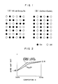
- Fig. 2 shows the relations between the composition and the bandgap of the alloy semiconductor and of the atomic layer superlattice semiconductor in the AlGaAs/GaAs system, which are plotted on the basis of the data provided by J.P. van der Ziel et al.
- the implementation thereof in the atomic layer superlattice increases the bandgap but provides entirely the same range of the bandgaps as the alloy semiconductor provides. For this reason, the above atomic layer superlattice do not have a merit of being applied to the device such as a semiconductor laser, and hence the phenomenon has not been so greatly noticed.
- the superlattice structure in accordance with this invention can provide a semiconductor structure having a bandgap different from the alloy semiconductor having the same composition as the equivalent average composition over the entire superlattice structure.
- the atomic layer superlattice one period of which is (ZnS) (CdS) (ZnS) (CdS) (ZnS) (CdS) and (CdS) is used as the clad layer, it can be lattice-matched with the GaAs substrate since its lattice constant is equal to the Zn 0.42 Cd 0.58 S alloy semiconductor and also it can provide an increased bandgap due to the increase of short range order.
- the above atomic lyaer superlattice in place of the Zn 0.42 Cd 0.58 S alloyed semiconductor stabilized lasing can be attained.
- Fig. 3a shows a lamination structure according to this embodiment.
- an undoped GaAs buffer layer 32 having a thickness of 0.1 ⁇ m is epitaxially grown on a semi-insulating (100) GaAs substrate 31.
- a clad layer 32 having a thickness of 0.5 ⁇ m which is constructed by an atomic layer superlattice having periods consisting of seven monolayers of (ZnS), (CdS), (ZnS), (CdS), (ZnS), (CdS) and (CdS).
- Fig. 3b schematically shows the lamination on pile-up state of the atomic layer superlattice in a cross section.
Landscapes
- Physics & Mathematics (AREA)
- Optics & Photonics (AREA)
- Condensed Matter Physics & Semiconductors (AREA)
- General Physics & Mathematics (AREA)
- Electromagnetism (AREA)
- Engineering & Computer Science (AREA)
- Nanotechnology (AREA)
- Chemical & Material Sciences (AREA)
- Biophysics (AREA)
- Crystallography & Structural Chemistry (AREA)
- Life Sciences & Earth Sciences (AREA)
- Semiconductor Lasers (AREA)
- Led Devices (AREA)
Abstract
An opto-electronic device has an atomic layer superlattice semiconductor comprising different semiconductor materials periodically piled up, each material having an atomic layer thickness. The superlattice semiconductor has a bandgap different from an alloy semiconductor having equivalently the same composition as the former.
In a semiconductor laser, as clad layers (33, 35; 43, 45), the atomic layer superlattice semiconductor having equivalently the same composition as a Zn0.42 Cd0.58 S alloy semiconductor and a larger bandgap than the later is used, and a ZnSe0.94 S0.06 alloy semiconductor as an active layer (34, 44) is located between the cladding layers. The double-hetero structure semiconductor laser thus provided can perform the lasing at 470 nm at room temperature.
Description
- This invention relates to an opto-electronic device and more particularly to a visible light semiconductor laser having a wide lasing wavelength range.
- Semiconductor lasers having a shorter lasing wavelength have been required mainly in the technical field of optical information processing. However, the AlGaAs/GaAs system which is now prevalently used can not easily provide the lasing at the wavelength lower than 720 nm due to its bandgap value. Thus, the AlGaInP/GaAs system laser has been noticed in place of the AlGaAs/GaAs system and will be put to practice use in the near future. However, this material also, due to its bandgap value can not easily provide the lasing of yellow, green, blue, etc. at the wavelength lower than 600 nm. This AlGaInP/GaAs system is now generally considered to be a material which can provide the shortest wavelength lasing among III-V alloy semiconductor materials, as disclosed in J. Appl. Phys. Vol. 58, 1982, page 4928. This means that the semiconductor laser using the ordinary III-V alloy semiconductor material can not provide the lasing at the wavelength lower than 600 nm, i.e. the lasing of yellow, green, and blue other than red.
- On the other hand, development of the crystal growth such as MBE (Molecular Beam Epitaxy), OMVPE (Organo Metallic Vapor Phase Epitaxy), etc. has enable the layer thickness in an atomic layer to be controlled. Fig. 1 shows schematic diagrams of the atomic arrangement on the column III sublattice of an Al0.5Ga0.5As alloy semiconductor and of an atomic layer superlattice semiconductor in which AlAs and GaAs are piled in each monolayer which is hereinafter referred to (AlAs)₁ (GaAs)₁. As understood from this figure, the superlattice semiconductor having the period on the order of an atomic layer thickness is different from the alloy semiconductor having equivalently the same composition in their electronic energy structure, i.e., bandgap since they have the same average composition but different short range orders and symmetries. For example, J.P. van der Ziel et al report in J. Appl. Phys. Vol. 48, 1977, page 3108 that in the AlGaAs/GaAs system, the atomic layer superlattice semiconductor has a bandgap greater than the alloy semiconductor by about 100 meV. T. Nakayama et al. report the theoretical analysis of this phenomenon in J. Phys. Soc. Jpn. Vol. 54, 1985, pages 4726-4734.
- Fig. 2 shows the relations between the composition and the bandgap of the alloy semiconductor and of the atomic layer superlattice semiconductor in the AlGaAs/GaAs system, which are plotted on the basis of the data provided by J.P. van der Ziel et al. As seen from the figure, with respect to the AlGaAs/GaAs system, the implementation thereof in the atomic layer superlattice increases the bandgap but provides entirely the same range of the bandgaps as the alloy semiconductor provides. For this reason, the above atomic layer superlattice do not have a merit of being applied to the device such as a semiconductor laser, and hence the phenomenon has not been so greatly noticed.
- Further, the phenomenon that the superlattice semiconductor having the period on the atomic layer thickness level has a bandgap greater than the alloy semiconductor having equivalently the same composition as the former has not been demonstrated about the material other than the AlGaAs/GaAs system. This is considered because ① as mentioned above, the application thereof does not have a great merit and so the phenomenon has been unconcerned, ② the basic crystallization technique on the AlGaAs/GaAs system, which has been researched most eagerly, has been already established, ③ the AlGaAs/GaAs system, the component materials (AlAs and GaAs) of which have the bond length equal to each other, is much easier to grow the crystal than the other system the component materials of which have different bond lengths and so the material having a complicated composition has not been required, etc.
- On the other hand, the inventors of this invention payed their attention to the above phenomenon and investigated the material system which is applicable to an opto-electronic device, particularly a visible light semiconductor laser.
- An object of this invention is to provide a semiconductor device having a superlattice structure implemented on a predetermined substrate, which has a bandgap that could not be realized using ordinary alloy semiconductors.
- The superlattice structure in accordance with this invention can provide a semiconductor structure having a bandgap different from the alloy semiconductor having the same composition as the equivalent average composition over the entire superlattice structure.
- The superlattice structure according to this invention is configured as follows and hereinafter referred to as an atomic layer superlattice.
- The different kinds of semiconductor layers comprising from one to ten monolayers are piled up. The layer exceeding ten monolayers strongly reveals the intrinsic nature of the semiconductor materials and thus provides the effect of the pile-up of the semiconductor layers. The semiconductor is composed of at least binary compound. The typical examples thereof are III-V compound semiconductor and II-VI compound semiconductor. More concretely, the III-V compound semiconductor is InP, GaP, InAs, GaAs, AlAs, AlP, etc., and the II-VI compound semiconductor is ZnSe, ZnTe, ZnS, CdTe, etc. Of course, the binary compound is most preferable in this invention. The term "monolayer" in this specification means one layer unit of the compound semiconductor of each semiconductor layers mentioned above, e.g. InP.
- The equivalent bandgap of the superlattice structure according to this invention is adjusted by the selection of the average composition the entire semiconductor structure having the superlattice structure and the number of the unit monolayers. The theoretical analysis of the above adjustment is disclosed in e.g. Journal of the Physical Society of Japan, Vol. 54, No. 12, December 1985, pp, 4726 to 4734. Incidentally, the crystal growth can be carried out through the techniques of MBE (Molecular Beam Epitaxial Method) and OMVPE (Oregano Metallic Vapor Phase Epitaxy).
- Thus, the above object can be attained by a superlattice structure formed by piling up the semiconductor layers of the component materials with a very short period of 1 to 10 monolayers in each semiconductor layer. However, some materials, due to the problem of change of their transition type, do not necessarily have the greatest bandgap when each semiconductor layer is provided by one monolayer
the same composition. Otherwise, they may have the greatest bandgap when each semiconductor layer is provided by two or three monolayers. - Further, on the contrary, some superlattice materials, when the monolayers of the component materials are piled with a slightly long period of about 6 monolayers, can provide a bandgap smaller than the alloy semiconductor having the same composition as the former.
- In this way, the atomic layer superlattice according to this invention can implement on a predetermined substrate the bandgap of the magnitude which the ordinary alloyed semiconductor could not implement. This advantage can be applied to several opto-electronic devices such as a semiconductor laser, a light emitting diode, a light receiving device, a composite device thereof, etc.
- In the case where this invention is applied to the semiconductor laser, the atomic layer superlattice may be used as either an active layer or a clad layer. The use thereof as the active layer enables the lasing at the wavelength which could not be realized by the semiconductor laser constructed by only the ordinary alloy semiconductor. Also, the use thereof as the clad layer permits the difference in a bandgap between the active layer and the clad layer to be realized in accordance with the design requirement of a device.
- A typical example of the application of this application to the semiconductor laser is a double-hetero laser including an acitve layer made of ZnSe0.94S0.06, which is in lattice-match with a GaAs substrate, and a clad layer made of Zn0.42Cd0.58S. Since the active layer ZnSe0.94S0.06 has a bandgap of 2.7 eV of a direct transition type, the lasing of blue at the wavelength of 470 nm or so can be exposed. However, since the clad layer Zn0.42Cd0.58S has a bandgap of 2.9 eV which is very slighly different from that in the active layer, the lasing at room temperature can not be easily realized.
- On the other hand, if the atomic layer superlattice one period of which is (ZnS) (CdS) (ZnS) (CdS) (ZnS) (CdS) and (CdS) is used as the clad layer, it can be lattice-matched with the GaAs substrate since its lattice constant is equal to the Zn0.42Cd0.58S alloy semiconductor and also it can provide an increased bandgap due to the increase of short range order. Therefore, by using as the clad layer, the above atomic lyaer superlattice in place of the Zn0.42Cd0.58S alloyed semiconductor, stabilized lasing can be attained.
- Accordingly, the atomic layer superlattice according to this invention can be effectively adapted to many other systems which can not provide the lasing in a visible light range because the alloy semiconductor used as the clad layer has a small bandgap.
-
- Fig. 1 is schematic diagrams of the column III atom arrangement of an Al0.5Ga0.5As alloy and (AlAs)₁(GaAs)₁ superlattice semiconductor;
- Fig. 2 is a graph showing the relations between the composition and the bandgap of an alloy semiconductor and of an atomic layer super-lattice semiconductor in an AlGaAs/GaAs system.
- Fig. 3a is a sectional view of a semiconductor laser device according to a first embodiment of this invention;
- Fig. 3b is a partially enlarged sectional view of the
clad layer 33 in Fig. 3b; and - Fig. 4 is a sectional view of a semiconductor laser device according to a second embodiment of this invention.
- Fig. 3a shows a lamination structure according to this embodiment. First, an undoped
GaAs buffer layer 32 having a thickness of 0.1 µm is epitaxially grown on a semi-insulating (100)GaAs substrate 31. Aclad layer 32 having a thickness of 0.5 µm which is constructed by an atomic layer superlattice having periods consisting of seven monolayers of (ZnS), (CdS), (ZnS), (CdS), (ZnS), (CdS) and (CdS). Fig. 3b schematically shows the lamination on pile-up state of the atomic layer superlattice in a cross section. A ZnSe0.94S0.06 alloy semiconductor 34 of 0.1 µm, which constitutes an active layer, is epitaxially grown on the clad layer. Finally, another cladlayer 35 of 0.5 µm is epitaxially grown on the active layer 34. The respective epitaxial layers 32 to 35 are piled up in an atomic layer epitaxial growth system improved on MBE (Molecular Beam Epitaxy) device by alternately opening and closing, for each atomic layer, the shutter of a column II (or III) atom cell and the shutter of a column VI (or V) atom cell. This is carried out monitoring the intensity of RHEED. The active layer ZnSeS is formed to be an alloy semiconductor by simultaneously opening and closing the cells of Se and S. The double-hetero structure wafer thus provided is formed in a chip having a size of 300 × 500 (µm)² by means of cleavage. The cleavage plane constitutes the resonator end surface of the semiconductor laser. The semiconductor laser thus provided permits the lasing at 470 nm at room temperature by optically pumping by a dye laser having a lasing wavelength of 400 nm. In this embodiment, the doping into the epitaxial layers is not performed since the optical pumping permits lasing. Of course, a semiconductor laser of an ordinary current injection type can be constituted. Incidentally, the pile-up state in the superlattice was recognized by a transmission electron microscope. - In this embodiment, this invention is applied to a current injection type semiconductor laser. The atomic layer superlattice is used as the clad layer of the semiconductor laser.
- Fig. 4 shows the sectional structure of the current injection type semiconductor laser. First, a Se-doped n-type
GaAs buffer layer 42 of 0.1 µm is epitaxially grown on an n-type (100) GaAs substrate. Aclad layer 43 of 1 µm which is an atomic layer superlattice formed by alternately piling up two n-type InP monolayers and two n-type AlP monolayers (these monolayers are Se-doped) is epitaxially grown on thebuffer layer 42. An un-doped Al0.25Ga0.25In0.5P alloy semiconductor 44 of 0.1 µm which constitutes an active layer is epitaxially grown on the cladlayer 43. Another atomic layer superlattice cladlayer 45 of 1 µm which is formed by alternately piling up two p-type InP monolyaers and two p-type AlP monolayers (these monolayers are Zn-doped) is epitaxially grown on theactive layer 44. Finally, a Zn-doped p-type GaAs 46 of 0.5 µm which serves as a cap layer is epitaxially grown on the cladlayer 45. The respective epitaxial layers 42 to 46 were successively grown by an OMVPE (Organo Metallic Vapor Phase Epitaxy) device which can provide an abrupt hetero-interface in the atomic layer by moving a substrate within two reactors. The n-type and the p-type carrier concentration was fixed to 1 × 10¹⁸cm⁻³. Formed on the double-hetero structure wafer thus provided are an SiO₂current blocking layer 47 and ohmic-electrodes Embodiment 1. Further, although Al0.25Ga0.25In0.5P was used as the active layer in this embodiment, (AlxGa1-x)0.5In0.5P(0 ≦ x ≦ 0.7), which is in lattice-match with the GaAs substrate may be used. - Table 1 shows examples of the semiconductor laser which can be fabricated in the manner like this embodiment. As apparent from the Table, lasing of yellow, green, yellow green, etc. which could not implemented by the prior art can be realized.

- In accordance with this invention, the superlattice semiconductor formed by periodically piling up different semiconductor materials each with an atomic layer thickness level can provide a bandgap different from the alloy semiconductor having equivalently the same composition as the former, thereby implementing a device sach as a visible light semiconductor laser which could not be realized using the ordinary alloy semiconductor.
Claims (9)
1. An opto-electronic device having a superlattice semiconductor (33, 43, 35, 45) comprising different semiconductor material layers periodically piled up, each layer having a thickness of 1 to 10 monolayers.
2. An opto-electronic device having a superlattice semiconductor comprising different semiconductor material layers periodically piled up, each layer having a thickness of 1 to 10 monolayers, said superlattice semiconductor having a bandgap different from an alloy semiconductor having equivalently the same composition as the former.
3. An opto-electronic device according to Claim 2, wherein said superlattice semiconductor having a bandgap larger than the alloy semiconductor having equivalently the same composition as the former.
4. An opto-electronic device according to Claim 2, wherein said superlattice semiconductor is constituted by piling up layers of different II-VI binary semiconductors.
5. An opto-electronic device according to Claim 2, wherein said superlattice semiconductor is one selected from the group consisting of a ZnCdS system, ZnTeSe system and AlGaInP system.
6. An opto-electronic device according to Claim 2, wherein said opto-electronic device is a double-hetero structure semiconductor laser, and said superlattice semiconductor is a clad layer.
7. An opto-electronic device according to Claim 6, wherein said double-hetero structure semiconductor laser comprises a first conduction type GaAs substrate (31, 41), a first conduction type GaAs buffer layer (32, 42) formed on said GaAs substrate, a first clad layer (33, 43) of said superlattice semiconductor of a first conduction type which is formed on said GaAs buffer layer, an (AlxGa1-x)0.5In0.5P (0 ≦ x ≦ 0.7) active layer (34, 44) formed on said first clad layer and having a smaller bandgap and a larger refractive index than said first clad layer, a second clad layer (35, 45) of said superlattice semiconductor of a second conduction type opposite to said first conduction type, having a larger bandgap and a smaller refractive index than said active layer, which is formed on said active layter, and electrodes (48, 49) electrically connected with said layers of the first conduction type and the second conduction type, and the superlattice semiconductor of said first and second clad layers is formed by alternately piling up two InP monolayers and two AlP monolayers.
8. An opto-electronic device according to Claim 1 or 2, wherein said opto-electronic device is a double-hetero structure semiconductor laser, said superlattice semiconductor is an active layer and the bandgap of the superlattice semiconductor is smaller than the alloy semiconductor having equivalently the same composition as the former.
9. An opto-electronic device according to Claim 8, wherein said double-hetero structure semiconductor laser comprises a first conduction type GaAs substrate (31, 41), a first clad layer (33, 43) of a first conduction type ZnSe formed on said GaAs substrate, an active layer of said superlattice semiconductor having a smaller bandgap and a refractive index than said first clad layer, which is formed on said first clad layer, a second clad layer (35, 45) of a second conduction type ZnSe formed on said active layer, having a larger bandgap and a smaller refractive index than said active layer, and electrodes electrically connected with said clad layers of the first conduction type and the second conduction type, and the superlattice semiconductor of said active layer has one period consisting of (InP), (GaP), (InP), (AlP), (InP), and (AlP) each of which corresponds a monolayer.
Applications Claiming Priority (2)
| Application Number | Priority Date | Filing Date | Title |
|---|---|---|---|
| JP68830/87 | 1987-03-25 | ||
| JP6883087A JP2544378B2 (en) | 1987-03-25 | 1987-03-25 | Optical semiconductor device |
Publications (2)
| Publication Number | Publication Date |
|---|---|
| EP0284031A2 true EP0284031A2 (en) | 1988-09-28 |
| EP0284031A3 EP0284031A3 (en) | 1989-03-29 |
Family
ID=13385011
Family Applications (1)
| Application Number | Title | Priority Date | Filing Date |
|---|---|---|---|
| EP88104589A Ceased EP0284031A3 (en) | 1987-03-25 | 1988-03-22 | Opto-electronic device |
Country Status (4)
| Country | Link |
|---|---|
| US (1) | US4794606A (en) |
| EP (1) | EP0284031A3 (en) |
| JP (1) | JP2544378B2 (en) |
| KR (1) | KR910003465B1 (en) |
Cited By (7)
| Publication number | Priority date | Publication date | Assignee | Title |
|---|---|---|---|---|
| EP0395392A3 (en) * | 1989-04-28 | 1991-09-11 | Kabushiki Kaisha Toshiba | Semiconductor laser using five-element compound semiconductor |
| EP0400559A3 (en) * | 1989-05-31 | 1991-12-27 | Hitachi, Ltd. | Semiconductor optical device |
| EP0502442A3 (en) * | 1991-02-28 | 1993-02-03 | Omron Corporation | Semiconductor luminous element and superlattice structure |
| WO1993024979A1 (en) * | 1992-05-22 | 1993-12-09 | Minnesota Mining And Manufacturing Company | Ii-vi laser diodes with quantum wells grown by atomic layer epitaxy and migration enhanced epitaxy |
| US5289486A (en) * | 1991-02-28 | 1994-02-22 | Omron Corporation | Semiconductor luminous element and superlattice structure |
| EP0637862A3 (en) * | 1993-08-05 | 1995-05-24 | Hitachi Ltd | Semiconductor laser device and manufacturing method. |
| EP0696094A4 (en) * | 1992-12-28 | 1995-11-28 | Np Predpr Principia Optics | Laser electron-beam tube |
Families Citing this family (14)
| Publication number | Priority date | Publication date | Assignee | Title |
|---|---|---|---|---|
| US4786951A (en) * | 1985-02-12 | 1988-11-22 | Mitsubishi Denki Kabushiki Kaisha | Semiconductor optical element and a process for producing the same |
| JPS63245984A (en) * | 1987-04-01 | 1988-10-13 | Seiko Epson Corp | Semiconductor light emitting device and its manufacturing method |
| NL8701497A (en) * | 1987-06-26 | 1989-01-16 | Philips Nv | SEMICONDUCTOR DEVICE FOR GENERATING ELECTROMAGNETIC RADIATION. |
| US5198690A (en) * | 1990-11-26 | 1993-03-30 | Sharp Kabushiki Kaisha | Electroluminescent device of II-IV compound semiconductor |
| JP2784093B2 (en) * | 1991-02-21 | 1998-08-06 | 星和電機株式会社 | Semiconductor device |
| US5375134A (en) * | 1991-02-21 | 1994-12-20 | Sony Corporation | Semiconductor light emitting device |
| EP0544357B1 (en) * | 1991-11-26 | 1996-09-04 | Koninklijke Philips Electronics N.V. | Radiation-emitting semiconductor diode |
| RU2064206C1 (en) * | 1991-12-26 | 1996-07-20 | Физический институт им.П.Н.Лебедева РАН | Laser screen for cathode-ray tube and method for its manufacturing |
| KR950007490B1 (en) * | 1991-12-28 | 1995-07-11 | 엘지전자주식회사 | Semiconductor laser |
| US5515393A (en) * | 1992-01-29 | 1996-05-07 | Sony Corporation | Semiconductor laser with ZnMgSSe cladding layers |
| JPH06104533A (en) * | 1992-09-22 | 1994-04-15 | Matsushita Electric Ind Co Ltd | Blue light emitting device and manufacturing method thereof |
| US5260957A (en) * | 1992-10-29 | 1993-11-09 | The Charles Stark Draper Laboratory, Inc. | Quantum dot Laser |
| US5363395A (en) * | 1992-12-28 | 1994-11-08 | North American Philips Corporation | Blue-green injection laser structure utilizing II-VI compounds |
| US5879962A (en) * | 1995-12-13 | 1999-03-09 | Minnesota Mining And Manufacturing Company | III-V/II-VI Semiconductor interface fabrication method |
Family Cites Families (14)
| Publication number | Priority date | Publication date | Assignee | Title |
|---|---|---|---|---|
| US4205329A (en) * | 1976-03-29 | 1980-05-27 | Bell Telephone Laboratories, Incorporated | Periodic monolayer semiconductor structures grown by molecular beam epitaxy |
| US4122407A (en) * | 1976-04-06 | 1978-10-24 | International Business Machines Corporation | Heterostructure junction light emitting or responding or modulating devices |
| US4261771A (en) * | 1979-10-31 | 1981-04-14 | Bell Telephone Laboratories, Incorporated | Method of fabricating periodic monolayer semiconductor structures by molecular beam epitaxy |
| JPS57187986A (en) * | 1981-05-15 | 1982-11-18 | Nippon Telegr & Teleph Corp <Ntt> | Semiconductor light emitting element |
| NL8301215A (en) * | 1983-04-07 | 1984-11-01 | Philips Nv | SEMICONDUCTOR DEVICE FOR GENERATING ELECTROMAGNETIC RADIATION. |
| US4695857A (en) * | 1983-06-24 | 1987-09-22 | Nec Corporation | Superlattice semiconductor having high carrier density |
| US4671830A (en) * | 1984-01-03 | 1987-06-09 | Xerox Corporation | Method of controlling the modeling of the well energy band profile by interdiffusion |
| JPS6110293A (en) * | 1984-06-25 | 1986-01-17 | Sharp Corp | Photo semiconductor device |
| JPH0728079B2 (en) * | 1984-07-26 | 1995-03-29 | 新技術事業団 | Method for manufacturing semiconductor laser |
| JPH0728080B2 (en) * | 1984-09-25 | 1995-03-29 | 日本電気株式会社 | Semiconductor superlattice structure |
| JPS61113738A (en) * | 1984-11-09 | 1986-05-31 | Tokai Carbon Co Ltd | Low density whisker forming body for composite material, and its production |
| JPH0669109B2 (en) * | 1984-12-07 | 1994-08-31 | シャ−プ株式会社 | Optical semiconductor device |
| JPS61137383A (en) * | 1984-12-07 | 1986-06-25 | Sharp Corp | Photosemiconductor device |
| US4731338A (en) * | 1986-10-09 | 1988-03-15 | Amoco Corporation | Method for selective intermixing of layered structures composed of thin solid films |
-
1987
- 1987-03-25 JP JP6883087A patent/JP2544378B2/en not_active Expired - Lifetime
-
1988
- 1988-03-18 KR KR1019880002879A patent/KR910003465B1/en not_active Expired
- 1988-03-22 EP EP88104589A patent/EP0284031A3/en not_active Ceased
- 1988-03-24 US US07/172,502 patent/US4794606A/en not_active Expired - Lifetime
Cited By (10)
| Publication number | Priority date | Publication date | Assignee | Title |
|---|---|---|---|---|
| EP0395392A3 (en) * | 1989-04-28 | 1991-09-11 | Kabushiki Kaisha Toshiba | Semiconductor laser using five-element compound semiconductor |
| EP0400559A3 (en) * | 1989-05-31 | 1991-12-27 | Hitachi, Ltd. | Semiconductor optical device |
| EP0502442A3 (en) * | 1991-02-28 | 1993-02-03 | Omron Corporation | Semiconductor luminous element and superlattice structure |
| US5289486A (en) * | 1991-02-28 | 1994-02-22 | Omron Corporation | Semiconductor luminous element and superlattice structure |
| WO1993024979A1 (en) * | 1992-05-22 | 1993-12-09 | Minnesota Mining And Manufacturing Company | Ii-vi laser diodes with quantum wells grown by atomic layer epitaxy and migration enhanced epitaxy |
| US5395791A (en) * | 1992-05-22 | 1995-03-07 | Minnesota Mining And Manufacturing Company | Growth of II VI laser diodes with quantum wells by atomic layer epitaxy and migration enhanced epitaxy |
| US6057559A (en) * | 1992-05-22 | 2000-05-02 | 3M Innovative Properties Company | II-VI laser diodes with short-period strained-layer superlattice quantum wells |
| EP0696094A4 (en) * | 1992-12-28 | 1995-11-28 | Np Predpr Principia Optics | Laser electron-beam tube |
| US5687185A (en) * | 1992-12-28 | 1997-11-11 | Principia Optics, Inc. | Laser cathode-ray tube |
| EP0637862A3 (en) * | 1993-08-05 | 1995-05-24 | Hitachi Ltd | Semiconductor laser device and manufacturing method. |
Also Published As
| Publication number | Publication date |
|---|---|
| KR910003465B1 (en) | 1991-05-31 |
| JPS63236387A (en) | 1988-10-03 |
| KR880011962A (en) | 1988-10-31 |
| JP2544378B2 (en) | 1996-10-16 |
| US4794606A (en) | 1988-12-27 |
| EP0284031A3 (en) | 1989-03-29 |
Similar Documents
| Publication | Publication Date | Title |
|---|---|---|
| US4794606A (en) | Opto-electronic device | |
| EP0446764B1 (en) | Quaternary II-VI semiconductor material for photonic device | |
| US5251225A (en) | Quantum-well diode laser | |
| US5075743A (en) | Quantum well optical device on silicon | |
| Nuese | III-V alloys for optoelectronic applications | |
| EP0103415B1 (en) | Light-emitting semiconductor devices and methods of producing the same | |
| EP0378919B1 (en) | High band-gap opto-electronic device and method for making same | |
| US5204284A (en) | Method of making a high band-gap opto-electronic device | |
| EP0605051A1 (en) | Blue-green injection laser structure | |
| JPH0418476B2 (en) | ||
| US7141829B2 (en) | Semiconductor laser device with antimony and crystal growth method | |
| Kressel | The application of heterojunction structures to optical devices | |
| JPH0821748B2 (en) | Semiconductor laser device | |
| Kimura et al. | Improvement of InP crystal quality grown on GaAs substrates and device applications | |
| EP1008189B1 (en) | II-VI SEMICONDUCTOR DEVICE WITH BeTe BUFFER LAYER | |
| EP0610893B1 (en) | Laser diode | |
| EP0403153B1 (en) | A method for forming a heteroepitaxial structure | |
| EP0293000B1 (en) | Light emitting device | |
| JPH1117219A (en) | DH structure semiconductor light emitting device | |
| EP0564915B1 (en) | Methods for growing compound semiconductor layers | |
| JP2586349B2 (en) | Semiconductor light emitting device | |
| JPH03236276A (en) | Optical functional element | |
| JPH0371679A (en) | Semiconductor light emitting element | |
| JP2661576B2 (en) | Semiconductor light emitting device | |
| Kressel et al. | Light sources |
Legal Events
| Date | Code | Title | Description |
|---|---|---|---|
| PUAI | Public reference made under article 153(3) epc to a published international application that has entered the european phase |
Free format text: ORIGINAL CODE: 0009012 |
|
| AK | Designated contracting states |
Kind code of ref document: A2 Designated state(s): DE FR |
|
| PUAL | Search report despatched |
Free format text: ORIGINAL CODE: 0009013 |
|
| AK | Designated contracting states |
Kind code of ref document: A3 Designated state(s): DE FR |
|
| 17P | Request for examination filed |
Effective date: 19890929 |
|
| 17Q | First examination report despatched |
Effective date: 19911219 |
|
| STAA | Information on the status of an ep patent application or granted ep patent |
Free format text: STATUS: THE APPLICATION HAS BEEN REFUSED |
|
| 18R | Application refused |
Effective date: 19941103 |