EP0284031A2 - Optoelektronische Vorrichtung - Google Patents
Optoelektronische Vorrichtung Download PDFInfo
- Publication number
- EP0284031A2 EP0284031A2 EP88104589A EP88104589A EP0284031A2 EP 0284031 A2 EP0284031 A2 EP 0284031A2 EP 88104589 A EP88104589 A EP 88104589A EP 88104589 A EP88104589 A EP 88104589A EP 0284031 A2 EP0284031 A2 EP 0284031A2
- Authority
- EP
- European Patent Office
- Prior art keywords
- semiconductor
- opto
- layer
- electronic device
- superlattice
- Prior art date
- Legal status (The legal status is an assumption and is not a legal conclusion. Google has not performed a legal analysis and makes no representation as to the accuracy of the status listed.)
- Ceased
Links
Images

Classifications
-
- H—ELECTRICITY
- H10—SEMICONDUCTOR DEVICES; ELECTRIC SOLID-STATE DEVICES NOT OTHERWISE PROVIDED FOR
- H10H—INORGANIC LIGHT-EMITTING SEMICONDUCTOR DEVICES HAVING POTENTIAL BARRIERS
- H10H20/00—Individual inorganic light-emitting semiconductor devices having potential barriers, e.g. light-emitting diodes [LED]
- H10H20/80—Constructional details
- H10H20/81—Bodies
- H10H20/811—Bodies having quantum effect structures or superlattices, e.g. tunnel junctions
- H10H20/812—Bodies having quantum effect structures or superlattices, e.g. tunnel junctions within the light-emitting regions, e.g. having quantum confinement structures
-
- B—PERFORMING OPERATIONS; TRANSPORTING
- B82—NANOTECHNOLOGY
- B82Y—SPECIFIC USES OR APPLICATIONS OF NANOSTRUCTURES; MEASUREMENT OR ANALYSIS OF NANOSTRUCTURES; MANUFACTURE OR TREATMENT OF NANOSTRUCTURES
- B82Y20/00—Nanooptics, e.g. quantum optics or photonic crystals
-
- H—ELECTRICITY
- H01—ELECTRIC ELEMENTS
- H01S—DEVICES USING THE PROCESS OF LIGHT AMPLIFICATION BY STIMULATED EMISSION OF RADIATION [LASER] TO AMPLIFY OR GENERATE LIGHT; DEVICES USING STIMULATED EMISSION OF ELECTROMAGNETIC RADIATION IN WAVE RANGES OTHER THAN OPTICAL
- H01S5/00—Semiconductor lasers
- H01S5/30—Structure or shape of the active region; Materials used for the active region
- H01S5/32—Structure or shape of the active region; Materials used for the active region comprising PN junctions, e.g. hetero- or double- heterostructures
-
- H—ELECTRICITY
- H01—ELECTRIC ELEMENTS
- H01S—DEVICES USING THE PROCESS OF LIGHT AMPLIFICATION BY STIMULATED EMISSION OF RADIATION [LASER] TO AMPLIFY OR GENERATE LIGHT; DEVICES USING STIMULATED EMISSION OF ELECTROMAGNETIC RADIATION IN WAVE RANGES OTHER THAN OPTICAL
- H01S5/00—Semiconductor lasers
- H01S5/30—Structure or shape of the active region; Materials used for the active region
- H01S5/34—Structure or shape of the active region; Materials used for the active region comprising quantum well or superlattice structures, e.g. single quantum well [SQW] lasers, multiple quantum well [MQW] lasers or graded index separate confinement heterostructure [GRINSCH] lasers
- H01S5/347—Structure or shape of the active region; Materials used for the active region comprising quantum well or superlattice structures, e.g. single quantum well [SQW] lasers, multiple quantum well [MQW] lasers or graded index separate confinement heterostructure [GRINSCH] lasers in AIIBVI compounds, e.g. ZnCdSe- laser
-
- H—ELECTRICITY
- H01—ELECTRIC ELEMENTS
- H01S—DEVICES USING THE PROCESS OF LIGHT AMPLIFICATION BY STIMULATED EMISSION OF RADIATION [LASER] TO AMPLIFY OR GENERATE LIGHT; DEVICES USING STIMULATED EMISSION OF ELECTROMAGNETIC RADIATION IN WAVE RANGES OTHER THAN OPTICAL
- H01S2302/00—Amplification / lasing wavelength
-
- H—ELECTRICITY
- H01—ELECTRIC ELEMENTS
- H01S—DEVICES USING THE PROCESS OF LIGHT AMPLIFICATION BY STIMULATED EMISSION OF RADIATION [LASER] TO AMPLIFY OR GENERATE LIGHT; DEVICES USING STIMULATED EMISSION OF ELECTROMAGNETIC RADIATION IN WAVE RANGES OTHER THAN OPTICAL
- H01S5/00—Semiconductor lasers
- H01S5/20—Structure or shape of the semiconductor body to guide the optical wave ; Confining structures perpendicular to the optical axis, e.g. index or gain guiding, stripe geometry, broad area lasers, gain tailoring, transverse or lateral reflectors, special cladding structures, MQW barrier reflection layers
- H01S5/2004—Confining in the direction perpendicular to the layer structure
-
- H—ELECTRICITY
- H01—ELECTRIC ELEMENTS
- H01S—DEVICES USING THE PROCESS OF LIGHT AMPLIFICATION BY STIMULATED EMISSION OF RADIATION [LASER] TO AMPLIFY OR GENERATE LIGHT; DEVICES USING STIMULATED EMISSION OF ELECTROMAGNETIC RADIATION IN WAVE RANGES OTHER THAN OPTICAL
- H01S5/00—Semiconductor lasers
- H01S5/20—Structure or shape of the semiconductor body to guide the optical wave ; Confining structures perpendicular to the optical axis, e.g. index or gain guiding, stripe geometry, broad area lasers, gain tailoring, transverse or lateral reflectors, special cladding structures, MQW barrier reflection layers
- H01S5/22—Structure or shape of the semiconductor body to guide the optical wave ; Confining structures perpendicular to the optical axis, e.g. index or gain guiding, stripe geometry, broad area lasers, gain tailoring, transverse or lateral reflectors, special cladding structures, MQW barrier reflection layers having a ridge or stripe structure
- H01S5/2205—Structure or shape of the semiconductor body to guide the optical wave ; Confining structures perpendicular to the optical axis, e.g. index or gain guiding, stripe geometry, broad area lasers, gain tailoring, transverse or lateral reflectors, special cladding structures, MQW barrier reflection layers having a ridge or stripe structure comprising special burying or current confinement layers
- H01S5/2214—Structure or shape of the semiconductor body to guide the optical wave ; Confining structures perpendicular to the optical axis, e.g. index or gain guiding, stripe geometry, broad area lasers, gain tailoring, transverse or lateral reflectors, special cladding structures, MQW barrier reflection layers having a ridge or stripe structure comprising special burying or current confinement layers based on oxides or nitrides
-
- H—ELECTRICITY
- H01—ELECTRIC ELEMENTS
- H01S—DEVICES USING THE PROCESS OF LIGHT AMPLIFICATION BY STIMULATED EMISSION OF RADIATION [LASER] TO AMPLIFY OR GENERATE LIGHT; DEVICES USING STIMULATED EMISSION OF ELECTROMAGNETIC RADIATION IN WAVE RANGES OTHER THAN OPTICAL
- H01S5/00—Semiconductor lasers
- H01S5/30—Structure or shape of the active region; Materials used for the active region
- H01S5/32—Structure or shape of the active region; Materials used for the active region comprising PN junctions, e.g. hetero- or double- heterostructures
- H01S5/3206—Structure or shape of the active region; Materials used for the active region comprising PN junctions, e.g. hetero- or double- heterostructures ordering or disordering the natural superlattice in ternary or quaternary materials
- H01S5/3207—Structure or shape of the active region; Materials used for the active region comprising PN junctions, e.g. hetero- or double- heterostructures ordering or disordering the natural superlattice in ternary or quaternary materials ordered active layer
-
- H—ELECTRICITY
- H01—ELECTRIC ELEMENTS
- H01S—DEVICES USING THE PROCESS OF LIGHT AMPLIFICATION BY STIMULATED EMISSION OF RADIATION [LASER] TO AMPLIFY OR GENERATE LIGHT; DEVICES USING STIMULATED EMISSION OF ELECTROMAGNETIC RADIATION IN WAVE RANGES OTHER THAN OPTICAL
- H01S5/00—Semiconductor lasers
- H01S5/30—Structure or shape of the active region; Materials used for the active region
- H01S5/32—Structure or shape of the active region; Materials used for the active region comprising PN junctions, e.g. hetero- or double- heterostructures
- H01S5/3211—Structure or shape of the active region; Materials used for the active region comprising PN junctions, e.g. hetero- or double- heterostructures characterised by special cladding layers, e.g. details on band-discontinuities
- H01S5/3216—Structure or shape of the active region; Materials used for the active region comprising PN junctions, e.g. hetero- or double- heterostructures characterised by special cladding layers, e.g. details on band-discontinuities quantum well or superlattice cladding layers
-
- H—ELECTRICITY
- H01—ELECTRIC ELEMENTS
- H01S—DEVICES USING THE PROCESS OF LIGHT AMPLIFICATION BY STIMULATED EMISSION OF RADIATION [LASER] TO AMPLIFY OR GENERATE LIGHT; DEVICES USING STIMULATED EMISSION OF ELECTROMAGNETIC RADIATION IN WAVE RANGES OTHER THAN OPTICAL
- H01S5/00—Semiconductor lasers
- H01S5/30—Structure or shape of the active region; Materials used for the active region
- H01S5/32—Structure or shape of the active region; Materials used for the active region comprising PN junctions, e.g. hetero- or double- heterostructures
- H01S5/323—Structure or shape of the active region; Materials used for the active region comprising PN junctions, e.g. hetero- or double- heterostructures in AIIIBV compounds, e.g. AlGaAs-laser, InP-based laser
- H01S5/32308—Structure or shape of the active region; Materials used for the active region comprising PN junctions, e.g. hetero- or double- heterostructures in AIIIBV compounds, e.g. AlGaAs-laser, InP-based laser emitting light at a wavelength less than 900 nm
- H01S5/32325—Structure or shape of the active region; Materials used for the active region comprising PN junctions, e.g. hetero- or double- heterostructures in AIIIBV compounds, e.g. AlGaAs-laser, InP-based laser emitting light at a wavelength less than 900 nm red laser based on InGaP
-
- H—ELECTRICITY
- H01—ELECTRIC ELEMENTS
- H01S—DEVICES USING THE PROCESS OF LIGHT AMPLIFICATION BY STIMULATED EMISSION OF RADIATION [LASER] TO AMPLIFY OR GENERATE LIGHT; DEVICES USING STIMULATED EMISSION OF ELECTROMAGNETIC RADIATION IN WAVE RANGES OTHER THAN OPTICAL
- H01S5/00—Semiconductor lasers
- H01S5/30—Structure or shape of the active region; Materials used for the active region
- H01S5/32—Structure or shape of the active region; Materials used for the active region comprising PN junctions, e.g. hetero- or double- heterostructures
- H01S5/327—Structure or shape of the active region; Materials used for the active region comprising PN junctions, e.g. hetero- or double- heterostructures in AIIBVI compounds, e.g. ZnCdSe-laser
-
- H—ELECTRICITY
- H01—ELECTRIC ELEMENTS
- H01S—DEVICES USING THE PROCESS OF LIGHT AMPLIFICATION BY STIMULATED EMISSION OF RADIATION [LASER] TO AMPLIFY OR GENERATE LIGHT; DEVICES USING STIMULATED EMISSION OF ELECTROMAGNETIC RADIATION IN WAVE RANGES OTHER THAN OPTICAL
- H01S5/00—Semiconductor lasers
- H01S5/30—Structure or shape of the active region; Materials used for the active region
- H01S5/34—Structure or shape of the active region; Materials used for the active region comprising quantum well or superlattice structures, e.g. single quantum well [SQW] lasers, multiple quantum well [MQW] lasers or graded index separate confinement heterostructure [GRINSCH] lasers
- H01S5/342—Structure or shape of the active region; Materials used for the active region comprising quantum well or superlattice structures, e.g. single quantum well [SQW] lasers, multiple quantum well [MQW] lasers or graded index separate confinement heterostructure [GRINSCH] lasers containing short period superlattices [SPS]
-
- H—ELECTRICITY
- H01—ELECTRIC ELEMENTS
- H01S—DEVICES USING THE PROCESS OF LIGHT AMPLIFICATION BY STIMULATED EMISSION OF RADIATION [LASER] TO AMPLIFY OR GENERATE LIGHT; DEVICES USING STIMULATED EMISSION OF ELECTROMAGNETIC RADIATION IN WAVE RANGES OTHER THAN OPTICAL
- H01S5/00—Semiconductor lasers
- H01S5/30—Structure or shape of the active region; Materials used for the active region
- H01S5/34—Structure or shape of the active region; Materials used for the active region comprising quantum well or superlattice structures, e.g. single quantum well [SQW] lasers, multiple quantum well [MQW] lasers or graded index separate confinement heterostructure [GRINSCH] lasers
- H01S5/3428—Structure or shape of the active region; Materials used for the active region comprising quantum well or superlattice structures, e.g. single quantum well [SQW] lasers, multiple quantum well [MQW] lasers or graded index separate confinement heterostructure [GRINSCH] lasers layer orientation perpendicular to the substrate
-
- H—ELECTRICITY
- H01—ELECTRIC ELEMENTS
- H01S—DEVICES USING THE PROCESS OF LIGHT AMPLIFICATION BY STIMULATED EMISSION OF RADIATION [LASER] TO AMPLIFY OR GENERATE LIGHT; DEVICES USING STIMULATED EMISSION OF ELECTROMAGNETIC RADIATION IN WAVE RANGES OTHER THAN OPTICAL
- H01S5/00—Semiconductor lasers
- H01S5/30—Structure or shape of the active region; Materials used for the active region
- H01S5/34—Structure or shape of the active region; Materials used for the active region comprising quantum well or superlattice structures, e.g. single quantum well [SQW] lasers, multiple quantum well [MQW] lasers or graded index separate confinement heterostructure [GRINSCH] lasers
- H01S5/343—Structure or shape of the active region; Materials used for the active region comprising quantum well or superlattice structures, e.g. single quantum well [SQW] lasers, multiple quantum well [MQW] lasers or graded index separate confinement heterostructure [GRINSCH] lasers in AIIIBV compounds, e.g. AlGaAs-laser, InP-based laser
- H01S5/34313—Structure or shape of the active region; Materials used for the active region comprising quantum well or superlattice structures, e.g. single quantum well [SQW] lasers, multiple quantum well [MQW] lasers or graded index separate confinement heterostructure [GRINSCH] lasers in AIIIBV compounds, e.g. AlGaAs-laser, InP-based laser with a well layer having only As as V-compound, e.g. AlGaAs, InGaAs
- H01S5/3432—Structure or shape of the active region; Materials used for the active region comprising quantum well or superlattice structures, e.g. single quantum well [SQW] lasers, multiple quantum well [MQW] lasers or graded index separate confinement heterostructure [GRINSCH] lasers in AIIIBV compounds, e.g. AlGaAs-laser, InP-based laser with a well layer having only As as V-compound, e.g. AlGaAs, InGaAs the whole junction comprising only (AI)GaAs
Definitions
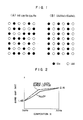
- Fig. 2 shows the relations between the composition and the bandgap of the alloy semiconductor and of the atomic layer superlattice semiconductor in the AlGaAs/GaAs system, which are plotted on the basis of the data provided by J.P. van der Ziel et al.
- the implementation thereof in the atomic layer superlattice increases the bandgap but provides entirely the same range of the bandgaps as the alloy semiconductor provides. For this reason, the above atomic layer superlattice do not have a merit of being applied to the device such as a semiconductor laser, and hence the phenomenon has not been so greatly noticed.
- the superlattice structure in accordance with this invention can provide a semiconductor structure having a bandgap different from the alloy semiconductor having the same composition as the equivalent average composition over the entire superlattice structure.
- the atomic layer superlattice one period of which is (ZnS) (CdS) (ZnS) (CdS) (ZnS) (CdS) and (CdS) is used as the clad layer, it can be lattice-matched with the GaAs substrate since its lattice constant is equal to the Zn 0.42 Cd 0.58 S alloy semiconductor and also it can provide an increased bandgap due to the increase of short range order.
- the above atomic lyaer superlattice in place of the Zn 0.42 Cd 0.58 S alloyed semiconductor stabilized lasing can be attained.
- Fig. 3a shows a lamination structure according to this embodiment.
- an undoped GaAs buffer layer 32 having a thickness of 0.1 ⁇ m is epitaxially grown on a semi-insulating (100) GaAs substrate 31.
- a clad layer 32 having a thickness of 0.5 ⁇ m which is constructed by an atomic layer superlattice having periods consisting of seven monolayers of (ZnS), (CdS), (ZnS), (CdS), (ZnS), (CdS) and (CdS).
- Fig. 3b schematically shows the lamination on pile-up state of the atomic layer superlattice in a cross section.
Landscapes
- Physics & Mathematics (AREA)
- Optics & Photonics (AREA)
- Condensed Matter Physics & Semiconductors (AREA)
- General Physics & Mathematics (AREA)
- Electromagnetism (AREA)
- Engineering & Computer Science (AREA)
- Nanotechnology (AREA)
- Chemical & Material Sciences (AREA)
- Biophysics (AREA)
- Crystallography & Structural Chemistry (AREA)
- Life Sciences & Earth Sciences (AREA)
- Semiconductor Lasers (AREA)
- Led Devices (AREA)
Applications Claiming Priority (2)
| Application Number | Priority Date | Filing Date | Title |
|---|---|---|---|
| JP68830/87 | 1987-03-25 | ||
| JP6883087A JP2544378B2 (ja) | 1987-03-25 | 1987-03-25 | 光半導体装置 |
Publications (2)
| Publication Number | Publication Date |
|---|---|
| EP0284031A2 true EP0284031A2 (de) | 1988-09-28 |
| EP0284031A3 EP0284031A3 (de) | 1989-03-29 |
Family
ID=13385011
Family Applications (1)
| Application Number | Title | Priority Date | Filing Date |
|---|---|---|---|
| EP88104589A Ceased EP0284031A3 (de) | 1987-03-25 | 1988-03-22 | Optoelektronische Vorrichtung |
Country Status (4)
| Country | Link |
|---|---|
| US (1) | US4794606A (de) |
| EP (1) | EP0284031A3 (de) |
| JP (1) | JP2544378B2 (de) |
| KR (1) | KR910003465B1 (de) |
Cited By (7)
| Publication number | Priority date | Publication date | Assignee | Title |
|---|---|---|---|---|
| EP0395392A3 (de) * | 1989-04-28 | 1991-09-11 | Kabushiki Kaisha Toshiba | Halbleiterlaser mit fünfelementigem Verbindungshalbleiter |
| EP0400559A3 (de) * | 1989-05-31 | 1991-12-27 | Hitachi, Ltd. | Optische Halbleitervorrichtung |
| EP0502442A3 (en) * | 1991-02-28 | 1993-02-03 | Omron Corporation | Semiconductor luminous element and superlattice structure |
| WO1993024979A1 (en) * | 1992-05-22 | 1993-12-09 | Minnesota Mining And Manufacturing Company | Ii-vi laser diodes with quantum wells grown by atomic layer epitaxy and migration enhanced epitaxy |
| US5289486A (en) * | 1991-02-28 | 1994-02-22 | Omron Corporation | Semiconductor luminous element and superlattice structure |
| EP0637862A3 (de) * | 1993-08-05 | 1995-05-24 | Hitachi Ltd | Halbleiterlaservorrichtung und Herstellungsverfahren. |
| EP0696094A4 (de) * | 1992-12-28 | 1995-11-28 | Np Predpr Principia Optics | Laserelektronenstrahlröhre |
Families Citing this family (14)
| Publication number | Priority date | Publication date | Assignee | Title |
|---|---|---|---|---|
| US4786951A (en) * | 1985-02-12 | 1988-11-22 | Mitsubishi Denki Kabushiki Kaisha | Semiconductor optical element and a process for producing the same |
| JPS63245984A (ja) * | 1987-04-01 | 1988-10-13 | Seiko Epson Corp | 半導体発光素子及びその製造方法 |
| NL8701497A (nl) * | 1987-06-26 | 1989-01-16 | Philips Nv | Halfgeleiderinrichting voor het opwekken van electromagnetische straling. |
| US5198690A (en) * | 1990-11-26 | 1993-03-30 | Sharp Kabushiki Kaisha | Electroluminescent device of II-IV compound semiconductor |
| JP2784093B2 (ja) * | 1991-02-21 | 1998-08-06 | 星和電機株式会社 | 半導体装置 |
| US5375134A (en) * | 1991-02-21 | 1994-12-20 | Sony Corporation | Semiconductor light emitting device |
| EP0544357B1 (de) * | 1991-11-26 | 1996-09-04 | Koninklijke Philips Electronics N.V. | Strahlung emittierende Halbleiterdiode |
| RU2064206C1 (ru) * | 1991-12-26 | 1996-07-20 | Физический институт им.П.Н.Лебедева РАН | Лазерный экран электронно-лучевой трубки и способ его изготовления |
| KR950007490B1 (ko) * | 1991-12-28 | 1995-07-11 | 엘지전자주식회사 | 반도체 레이저 |
| US5515393A (en) * | 1992-01-29 | 1996-05-07 | Sony Corporation | Semiconductor laser with ZnMgSSe cladding layers |
| JPH06104533A (ja) * | 1992-09-22 | 1994-04-15 | Matsushita Electric Ind Co Ltd | 青色発光素子およびその製造方法 |
| US5260957A (en) * | 1992-10-29 | 1993-11-09 | The Charles Stark Draper Laboratory, Inc. | Quantum dot Laser |
| US5363395A (en) * | 1992-12-28 | 1994-11-08 | North American Philips Corporation | Blue-green injection laser structure utilizing II-VI compounds |
| US5879962A (en) * | 1995-12-13 | 1999-03-09 | Minnesota Mining And Manufacturing Company | III-V/II-VI Semiconductor interface fabrication method |
Family Cites Families (14)
| Publication number | Priority date | Publication date | Assignee | Title |
|---|---|---|---|---|
| US4205329A (en) * | 1976-03-29 | 1980-05-27 | Bell Telephone Laboratories, Incorporated | Periodic monolayer semiconductor structures grown by molecular beam epitaxy |
| US4122407A (en) * | 1976-04-06 | 1978-10-24 | International Business Machines Corporation | Heterostructure junction light emitting or responding or modulating devices |
| US4261771A (en) * | 1979-10-31 | 1981-04-14 | Bell Telephone Laboratories, Incorporated | Method of fabricating periodic monolayer semiconductor structures by molecular beam epitaxy |
| JPS57187986A (en) * | 1981-05-15 | 1982-11-18 | Nippon Telegr & Teleph Corp <Ntt> | Semiconductor light emitting element |
| NL8301215A (nl) * | 1983-04-07 | 1984-11-01 | Philips Nv | Halfgeleiderinrichting voor het opwekken van electromagnetische straling. |
| DE3480631D1 (de) * | 1983-06-24 | 1990-01-04 | Nec Corp | Halbleiterstruktur mit uebergitter hoher traegerdichte. |
| US4671830A (en) * | 1984-01-03 | 1987-06-09 | Xerox Corporation | Method of controlling the modeling of the well energy band profile by interdiffusion |
| JPS6110293A (ja) * | 1984-06-25 | 1986-01-17 | Sharp Corp | 光半導体装置 |
| JPH0728079B2 (ja) * | 1984-07-26 | 1995-03-29 | 新技術事業団 | 半導体レ−ザの製造方法 |
| JPH0728080B2 (ja) * | 1984-09-25 | 1995-03-29 | 日本電気株式会社 | 半導体超格子構造体 |
| JPS61113738A (ja) * | 1984-11-09 | 1986-05-31 | Tokai Carbon Co Ltd | 複合材用低密度ウイスカ−成形体とその製造法 |
| JPH0669109B2 (ja) * | 1984-12-07 | 1994-08-31 | シャ−プ株式会社 | 光半導体装置 |
| JPS61137383A (ja) * | 1984-12-07 | 1986-06-25 | Sharp Corp | 光半導体装置 |
| US4731338A (en) * | 1986-10-09 | 1988-03-15 | Amoco Corporation | Method for selective intermixing of layered structures composed of thin solid films |
-
1987
- 1987-03-25 JP JP6883087A patent/JP2544378B2/ja not_active Expired - Lifetime
-
1988
- 1988-03-18 KR KR1019880002879A patent/KR910003465B1/ko not_active Expired
- 1988-03-22 EP EP88104589A patent/EP0284031A3/de not_active Ceased
- 1988-03-24 US US07/172,502 patent/US4794606A/en not_active Expired - Lifetime
Cited By (10)
| Publication number | Priority date | Publication date | Assignee | Title |
|---|---|---|---|---|
| EP0395392A3 (de) * | 1989-04-28 | 1991-09-11 | Kabushiki Kaisha Toshiba | Halbleiterlaser mit fünfelementigem Verbindungshalbleiter |
| EP0400559A3 (de) * | 1989-05-31 | 1991-12-27 | Hitachi, Ltd. | Optische Halbleitervorrichtung |
| EP0502442A3 (en) * | 1991-02-28 | 1993-02-03 | Omron Corporation | Semiconductor luminous element and superlattice structure |
| US5289486A (en) * | 1991-02-28 | 1994-02-22 | Omron Corporation | Semiconductor luminous element and superlattice structure |
| WO1993024979A1 (en) * | 1992-05-22 | 1993-12-09 | Minnesota Mining And Manufacturing Company | Ii-vi laser diodes with quantum wells grown by atomic layer epitaxy and migration enhanced epitaxy |
| US5395791A (en) * | 1992-05-22 | 1995-03-07 | Minnesota Mining And Manufacturing Company | Growth of II VI laser diodes with quantum wells by atomic layer epitaxy and migration enhanced epitaxy |
| US6057559A (en) * | 1992-05-22 | 2000-05-02 | 3M Innovative Properties Company | II-VI laser diodes with short-period strained-layer superlattice quantum wells |
| EP0696094A4 (de) * | 1992-12-28 | 1995-11-28 | Np Predpr Principia Optics | Laserelektronenstrahlröhre |
| US5687185A (en) * | 1992-12-28 | 1997-11-11 | Principia Optics, Inc. | Laser cathode-ray tube |
| EP0637862A3 (de) * | 1993-08-05 | 1995-05-24 | Hitachi Ltd | Halbleiterlaservorrichtung und Herstellungsverfahren. |
Also Published As
| Publication number | Publication date |
|---|---|
| EP0284031A3 (de) | 1989-03-29 |
| JP2544378B2 (ja) | 1996-10-16 |
| JPS63236387A (ja) | 1988-10-03 |
| KR910003465B1 (ko) | 1991-05-31 |
| KR880011962A (ko) | 1988-10-31 |
| US4794606A (en) | 1988-12-27 |
Similar Documents
| Publication | Publication Date | Title |
|---|---|---|
| EP0284031A2 (de) | Optoelektronische Vorrichtung | |
| EP0446764B1 (de) | Quaternäres II-VI-Halbleitermaterial für photonische Bauelemente | |
| US5251225A (en) | Quantum-well diode laser | |
| US5075743A (en) | Quantum well optical device on silicon | |
| Nuese | III-V alloys for optoelectronic applications | |
| EP0103415B1 (de) | Lichtemittierende Vorrichtungen und Verfahren zu deren Herstellung | |
| EP0378919B1 (de) | Optoelektronische Vorrichtung mit grossem Energiebandabstand und Herstellungsverfahren | |
| US5204284A (en) | Method of making a high band-gap opto-electronic device | |
| EP0605051A1 (de) | Im blau-grünen Bereich emittierender Injektionslaser | |
| JPH0418476B2 (de) | ||
| US7141829B2 (en) | Semiconductor laser device with antimony and crystal growth method | |
| Kressel | The application of heterojunction structures to optical devices | |
| JPH0821748B2 (ja) | 半導体レ−ザ装置 | |
| Kimura et al. | Improvement of InP crystal quality grown on GaAs substrates and device applications | |
| EP1008189B1 (de) | II-VI HALBLEITERVORRICHTUNG MIT BeTe-PUFFERSCHICHT | |
| EP0610893B1 (de) | Diodenlaser | |
| EP0403153B1 (de) | Verfahren zur Herstellung einer heteroepitaxialen Struktur | |
| EP0293000B1 (de) | Lichtemittierende Vorrichtung | |
| JPH1117219A (ja) | Dh構造半導体発光素子 | |
| EP0564915B1 (de) | Methoden für das Wachstum von Verbindungshalbleiterschichten | |
| JP2586349B2 (ja) | 半導体発光素子 | |
| JPH03236276A (ja) | 光機能素子 | |
| JPH0371679A (ja) | 半導体発光素子 | |
| JP2661576B2 (ja) | 半導体発光素子 | |
| Kressel et al. | Light sources |
Legal Events
| Date | Code | Title | Description |
|---|---|---|---|
| PUAI | Public reference made under article 153(3) epc to a published international application that has entered the european phase |
Free format text: ORIGINAL CODE: 0009012 |
|
| AK | Designated contracting states |
Kind code of ref document: A2 Designated state(s): DE FR |
|
| PUAL | Search report despatched |
Free format text: ORIGINAL CODE: 0009013 |
|
| AK | Designated contracting states |
Kind code of ref document: A3 Designated state(s): DE FR |
|
| 17P | Request for examination filed |
Effective date: 19890929 |
|
| 17Q | First examination report despatched |
Effective date: 19911219 |
|
| STAA | Information on the status of an ep patent application or granted ep patent |
Free format text: STATUS: THE APPLICATION HAS BEEN REFUSED |
|
| 18R | Application refused |
Effective date: 19941103 |