EP0284260B1 - Drucker vom Rasterabtasttyp - Google Patents
Drucker vom Rasterabtasttyp Download PDFInfo
- Publication number
- EP0284260B1 EP0284260B1 EP19880302170 EP88302170A EP0284260B1 EP 0284260 B1 EP0284260 B1 EP 0284260B1 EP 19880302170 EP19880302170 EP 19880302170 EP 88302170 A EP88302170 A EP 88302170A EP 0284260 B1 EP0284260 B1 EP 0284260B1
- Authority
- EP
- European Patent Office
- Prior art keywords
- data
- scan data
- printing
- scan
- storage section
- Prior art date
- Legal status (The legal status is an assumption and is not a legal conclusion. Google has not performed a legal analysis and makes no representation as to the accuracy of the status listed.)
- Expired - Lifetime
Links
Images

Classifications
-
- G—PHYSICS
- G06—COMPUTING OR CALCULATING; COUNTING
- G06K—GRAPHICAL DATA READING; PRESENTATION OF DATA; RECORD CARRIERS; HANDLING RECORD CARRIERS
- G06K15/00—Arrangements for producing a permanent visual presentation of the output data, e.g. computer output printers
- G06K15/02—Arrangements for producing a permanent visual presentation of the output data, e.g. computer output printers using printers
- G06K15/12—Arrangements for producing a permanent visual presentation of the output data, e.g. computer output printers using printers by photographic printing, e.g. by laser printers
- G06K15/128—Arrangements for producing a permanent visual presentation of the output data, e.g. computer output printers using printers by photographic printing, e.g. by laser printers generating or processing printable items, e.g. characters
-
- G—PHYSICS
- G06—COMPUTING OR CALCULATING; COUNTING
- G06K—GRAPHICAL DATA READING; PRESENTATION OF DATA; RECORD CARRIERS; HANDLING RECORD CARRIERS
- G06K15/00—Arrangements for producing a permanent visual presentation of the output data, e.g. computer output printers
- G06K15/02—Arrangements for producing a permanent visual presentation of the output data, e.g. computer output printers using printers
-
- G—PHYSICS
- G06—COMPUTING OR CALCULATING; COUNTING
- G06K—GRAPHICAL DATA READING; PRESENTATION OF DATA; RECORD CARRIERS; HANDLING RECORD CARRIERS
- G06K2215/00—Arrangements for producing a permanent visual presentation of the output data
- G06K2215/0002—Handling the output data
- G06K2215/0077—Raster outputting to the print element(s)
- G06K2215/008—Raster outputting to the print element(s) from more than one raster memory
Definitions
- This invention relates to a printing device and more particularly to a dot data output device for a raster scan type printer.
- raster scan type printers such as laser printers
- multiple dot data representing character print informations are stored in a bit image transfer bank, and then sequentially read out to be converted to a raster data by means of a shift register.
- a printing device such as scanner is driven to print the characters on a sheet-like recording medium.
- bit image transfer bank for storing multiple dot data can not be quickly operated to read out and write the dot data because it uses dynamic random access memory (DRAM) or static random access memory (SRAM), resulting in a problem when applied to a printing system requiring a high-speed operation of dot data reading and writing.
- DRAM dynamic random access memory
- SRAM static random access memory
- the central processing unit (CPU) for controlling dot data transfer receives an interrupt signal from a selector arranged to switch between the two bit image transfer banks upon every such switching operation, so that repeated operation with such interrupt signals would result in a degraded efficiency in the CPU operation. Further, since the CPU is unable to access the bit image transfer bank from which the bit data is being transferred to the shift register, it could not deal with any update or delete of dot data even though such change be required while transferring dot data to the shift register.
- a raster scan type printer comprising storage means for storing a plurality of scan data including dot data representing characters to be printed on a printing medium, control means for sequentially reading out a set of data for one scanning operation from said storage means in the order of scanning, and printing means, including a scanner for performing a scanning operation, for performing a printing operation in response to said set of data, characterised in that: said storage means comprises a dual port memory means including a first storage section for storing said plurality of scan data, and a second storage section for storing a specific set of scan data to be transferred to said printing means for a specific scanning operation, synchronisation generating means for detecting a predetermined position of the scanner of the printing means and for generating a synchronisation signal transfer means for reading out said specific set of scan data from said first storage section to said second storage section in response to said synchronisation signal.
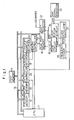
- a central processing unit (CPU) 11 comprises a program memory 12 sorting a control program and a work memory 13 which temporarily stores the operation results from CPU to perform operation processes in accordance with te control program.
- a font memory 14 stores dot data as aggregates of multiple dots which represents print information of characters and symbols.
- CPU 11 reads out any desired dot data from the font memory 14 to generate a 1-scan data, which is sent to a dual port memory 16 via a data address bus 15.
- the dual port memory 16 comprises a random access memory (RAM) 16a storing a print data and a serial access memory (SAM) 16b storing a 1-scan data.
- RAM random access memory
- SAM serial access memory
- RAM 16a (NEC UPD41264, TI TMS4461NL), constituted by a memory cell array of 256 x 4096 bits, is divided into row addresses from 0 to 255 and column addresses from 0 to 511.
- the 1-scan data 17 is devided into a fisrt non-image section 17a, an image section 17b, a continuous lighting section 17c, a transfer address section 17d and a second non-image section 17e.
- the image section 17b stores dot data to be printed on a certain dot area of a printing sheet or paper.
- the continuous lighting section 17c stores a data for instructing continued lighting of a luminous source to optically detect the operating position of the printing section in its scanning operation.
- the first and second non-image sections 17a and 17e and the transfer address section 17d store data which is not involved in dot printing. These sections are provided to set a timing for printing the dot data stored in the image section 17b on a certain dot area of the printing paper, as the 1-scan data is sequentially read out with sync signals.
- CPU 11 reads out a font data from the font memory 14 to generate a 1-scan data 17 which is to be stored in a certain row address of RAM 16a.
- SAM 16b consisting of 1 x 512 x 4 bits receives the respective 1-scan data from RAM 16a to be stored therein.
- CPU 11 outputs a row address data for specifying a specific row address stored in the dual port memory 16 to an address decoder 18.
- the address decoder 18 then transfers an address specified based on the row address data from CPU 11 to a memory controller 21.
- CPU 11 also delivers a starting address data for the data transfer to a transfer address decoder 19, which in turn generates a signal to the effect when receiving and detecting the starting address data.
- the memory controller 21 operates to set a timing for reading and writing of the 1-scan data 17 from RAM 16a and to SAM 16b as well as for transferring the 1-scan data 17 to the shift register 22, in accordance with these address data. This transfer operation takes place responsive to an output clock signal CL1.
- the shift register 22 receives the 1-scan data from SAM 16b of the dual port memory 16 through its serial port.
- the 1-scan data is output bit by bit to the scanner as a raster data, each time an image clock signal CL2 comes out while a load signal SG1 is being output.
- a sync signal generator 23 detects a predetermined position (home position) which the scanner passes by every time it performs one scanning operation, whereupon it sends a sync signal SYN to the interrupt controller 20, a flip-flop circuit 24 and a frequency divider 25.
- the flip-flop circuit 24 outputs a signal which closes a gate circuit 26 in response to the sync signal 24 and opens the circuit 26 in response to an inverse signal from the frequency divider 25.
- the frequency divider 25 is preset according to the sync signal SYN and counts the clock signals CL3 from a clock oscillator 27 to send an inverse signal to the flip-flop circuite 24 when a predetermined count is reached, that is a given period of time has passed.
- the frequency divider 25 demultiplies the clock signal CL3 from the clock oscillator 27 at a predetermined dividing ratio to generate the output clock signal CL1, the image clock signal CL2 and the load signal SG1, the former being transferred to the dual port memory 16 and the latter two to the shift register 22 via the gate circuit 26.
- CPU 11 reads out a dot data from the font memory 14 to generate a 1-scan data 17 required for one scanning operation of the scanner.
- the 1-scan data 17 is thus stored in RAM 16a of the dual port memory 16 such that the dot data corresponding to one scanning operation falls upon the image section 17b.
- CPU 11 sequentially generates 1-scan data 17 and transfers each of them to a specified row address in RAM 16a. Specifying the row address for a 1-scan data is achieved by sending an address data from CPU 11 to the address decoder 18.
- the interrupt controller 20 In response to the sync signal SYN the interrupt controller 20 sends an interrupt signal to the CPU 11.
- the transfer address decoder 19 and the address decoder 18 detects the starting transfer address to produce a signal for starting the transfer to the memory controller 21.
- the memory controller 21 then sends a transfer signal to the dual port memory 16 to transfer a 1-scan data 17 at the address of RAM 16a specified by the transfer address decoder 19 to SAM 16b.
- the flip-flop circuit 24 opens the gate circuit 26 in response to the inverse signal from the frequency divider 25 so that the output clock signal CL1 is delivered to the dual port memory 16 whereas the image clock signal CL2 and the load signal SG1 are transferred to the shift register 22 through the opened gate circuit 26.
- the 1-scan data in SAM 16b is sent to the shift register 22 in response to the output clock signal CL1.
- the 1-scan data 17 is serially output to the scanner from the shift register 22 in accordance with the image clock signal CL2.
- the data within the non-image section 17a of the 1-scan data 17 is first output sequentially in response to the image clock signal CL2. After the last bit of the data in the non-image section 17a has been output, the scanner reaches the print position of the printing paper, and thereafter the dot data within the image section 17b is output sequentially. As a result, the scanner prints dots on the printing paper in dependence on the dot data stored in the image section 17b being serially output.
- the luminuous source is turned on to optically detect the operating position of the scanner in scanning operation for synchronism with the succeeding scanning operation.
- a 1-scan data is sent from a specified row address in RAM 16a to SAM 16b and from SAM 16b to the shift register 22.
- the 1-scan data is then serially output from the shift register 22 to the scanner as a raster data.
- the dot data can be sequentially output to the scanner as a raster data, while at the same time a new 1-scan data is transferred to a given storage area.
- CPU 11 is allowed to access the dual port memory 16 during transfeering data to the shift register 22.
- fast printing is made possible without necessity of using more than one momery devices for a bit image transfer bank.
- an appropriate software enables CPU 11 to specify the row address in which the 1-scan data to be changed or deleted is stored. This embodiment is therefore able to cope with a requirement for data change or deletion, if it should happen during transferring dot data.
- the 1-scan data 17 corresponding to a dot data for one scanning operation is stored in each row address of RAM 16a. Accordingly, a dot data for one scanning operation can be read merely by specifying a corresponding row address, resulting in a simpler software for CPU 11 for transferring the 1-scan data 17. Since the 1-scan data 17 are divided into the non-image sections 17a and 17e, the image section 17b and the continuous lighting section 17c, location of the image section 17b accomodating the dot data for one scanning operation can be appropriately altered within the same 1-scan data 17, so that the timing at which the dot data is first output from the shift register to the scanner can be changed as desired.
- a modification of the invention can consist in that the 1-scan data 17 may comprise the dot data as print information only, while column addresses per row address in RAM 16a may store multiple 1-scan data 17 thus contracted.
Landscapes
- Engineering & Computer Science (AREA)
- Physics & Mathematics (AREA)
- General Engineering & Computer Science (AREA)
- General Physics & Mathematics (AREA)
- Theoretical Computer Science (AREA)
- Optics & Photonics (AREA)
- Dot-Matrix Printers And Others (AREA)
- Laser Beam Printer (AREA)
- Record Information Processing For Printing (AREA)
- Facsimile Scanning Arrangements (AREA)
- Image Input (AREA)
Claims (3)
- Drucker vom Rasterabtasttyp mit
Speichermittel (16) zum Speichern einer Mehrzahl von Abtastdaten einschließlich Punktdaten, die auf ein Druckmedium zu druckende Zeichen darstellen,
Steuermittel (11, 21) zum sequentiellen Auslesen eines Datensatzes für eine Abtasttätigkeit aus dem Speichermittel in der Reihenfolge des Abtastens,
und Druckmittel mit einem Abtaster zum Durchführen einer Abtasttätigkeit zum Ausführen einer Drucktätigkeit als Reaktion auf den Satz von Daten,
dadurch gkennzeichnet, daß das Speichermittel ein Dualportspeichermittel mit einem ersten Speicherabschnitt (16a) zum Speichern der Mehrzahl von Abtastdaten und einen zweiten Speicherabschnitt (16b) zum Speichern eines spezifischen Satzes von Daten, zu dem Druckmittel für eine spezifische Abtasttätigkeit zu übertragen ist, Synchronisationserzeugungsmittel zum Erfassen einer vorbestimmten Position des Abtasters des Druckmittels und zum Erzeugen eines Synchronisationssignales,
ein Übertragungsmittel zum Auslesen des spezifischen Satzes von Abtastdaten aus dem ersten Speicherabschnitt zu dem zweiten Speicherabschnitt als Reaktion auf das Synchronisationssignal aufweist. - Drucker nach Anspruch 1, bei dem jeder Satz von Daten Druckdaten (17b), die auf das Druckmedium zu druckende Punkte darstellen, und Nicht-Druckdaten (17a, 17c bis 17e) die vor und nach den Druckdaten angeordnet sind, aufweist.
- Drucker nach Anspruch 1 oder 2, bei dem der erste Speicherabschnitt in eine Mehrzahl von Zeilenadressen unterteilt ist und ein Satz von Abtastdaten in dem ein erster Speicherabschnitte an einer entsprechenden der Zeilenadressen gespeichert ist.
Applications Claiming Priority (2)
| Application Number | Priority Date | Filing Date | Title |
|---|---|---|---|
| JP62059871A JPH0780319B2 (ja) | 1987-03-14 | 1987-03-14 | ラスタ−スキヤン方式の印字装置 |
| JP59871/87 | 1987-03-14 |
Publications (3)
| Publication Number | Publication Date |
|---|---|
| EP0284260A2 EP0284260A2 (de) | 1988-09-28 |
| EP0284260A3 EP0284260A3 (en) | 1989-10-04 |
| EP0284260B1 true EP0284260B1 (de) | 1993-02-03 |
Family
ID=13125658
Family Applications (1)
| Application Number | Title | Priority Date | Filing Date |
|---|---|---|---|
| EP19880302170 Expired - Lifetime EP0284260B1 (de) | 1987-03-14 | 1988-03-11 | Drucker vom Rasterabtasttyp |
Country Status (3)
| Country | Link |
|---|---|
| EP (1) | EP0284260B1 (de) |
| JP (1) | JPH0780319B2 (de) |
| DE (1) | DE3877993T2 (de) |
Families Citing this family (1)
| Publication number | Priority date | Publication date | Assignee | Title |
|---|---|---|---|---|
| DE68920147T2 (de) * | 1989-10-12 | 1995-06-29 | Ibm | Anzeigesystem. |
Family Cites Families (3)
| Publication number | Priority date | Publication date | Assignee | Title |
|---|---|---|---|---|
| US3651258A (en) * | 1970-01-26 | 1972-03-21 | Bessemer Securities Corp | Method and apparatus for the formation of alpha-numerical characters on light sensitive surfaces |
| JPS61173951A (ja) * | 1985-01-29 | 1986-08-05 | Ricoh Co Ltd | 印字制御装置 |
| JPS61195865A (ja) * | 1985-02-27 | 1986-08-30 | Usac Electronics Ind Co Ltd | プリンタ制御方法 |
-
1987
- 1987-03-14 JP JP62059871A patent/JPH0780319B2/ja not_active Expired - Fee Related
-
1988
- 1988-03-11 DE DE19883877993 patent/DE3877993T2/de not_active Expired - Fee Related
- 1988-03-11 EP EP19880302170 patent/EP0284260B1/de not_active Expired - Lifetime
Also Published As
| Publication number | Publication date |
|---|---|
| JPS63224952A (ja) | 1988-09-20 |
| EP0284260A2 (de) | 1988-09-28 |
| JPH0780319B2 (ja) | 1995-08-30 |
| DE3877993D1 (de) | 1993-03-18 |
| DE3877993T2 (de) | 1993-06-03 |
| EP0284260A3 (en) | 1989-10-04 |
Similar Documents
| Publication | Publication Date | Title |
|---|---|---|
| US5021975A (en) | Printer with improved image printing function | |
| EP0137147B1 (de) | Musterverarbeitungssystem | |
| EP0551095B1 (de) | Serieller Rasterbilddrucker und Verfahren zu dessen Betrieb | |
| US6317193B2 (en) | Image forming apparatus | |
| JPS595434B2 (ja) | インサツソウチ | |
| US5360277A (en) | Label printer with selective memory update | |
| EP0452131B1 (de) | Ausgabeverfahren und -gerät | |
| JPH06119130A (ja) | 記録装置 | |
| EP0284260A2 (de) | Drucker vom Rasterabtasttyp | |
| JPS6035687B2 (ja) | プリントデ−タ制御装置 | |
| EP0397415A2 (de) | Drucker mit Abtastraster | |
| EP0072708B1 (de) | Drucker | |
| JPH0616764Y2 (ja) | ドットマトリクスプリンタ | |
| JP2564513B2 (ja) | プリンタ制御装置 | |
| JPH0383673A (ja) | 編集機能付きページプリンタ | |
| US5408592A (en) | Printer having a data output time controller | |
| US6014225A (en) | Frame buffer control method and circuit | |
| JP2908571B2 (ja) | ページプリンタ | |
| JP2924581B2 (ja) | プリンタのメモリ制御回路 | |
| JPH0515551B2 (de) | ||
| JP2715475B2 (ja) | 図形出力装置 | |
| JPS63252751A (ja) | 印字制御装置 | |
| JPH05212913A (ja) | 画像形成装置 | |
| JPH024915B2 (de) | ||
| JP3143118B2 (ja) | プリンタ及び印字イメージパターン展開方法 |
Legal Events
| Date | Code | Title | Description |
|---|---|---|---|
| PUAI | Public reference made under article 153(3) epc to a published international application that has entered the european phase |
Free format text: ORIGINAL CODE: 0009012 |
|
| AK | Designated contracting states |
Kind code of ref document: A2 Designated state(s): DE FR GB |
|
| PUAL | Search report despatched |
Free format text: ORIGINAL CODE: 0009013 |
|
| AK | Designated contracting states |
Kind code of ref document: A3 Designated state(s): DE FR GB |
|
| 17P | Request for examination filed |
Effective date: 19891009 |
|
| 17Q | First examination report despatched |
Effective date: 19910724 |
|
| GRAA | (expected) grant |
Free format text: ORIGINAL CODE: 0009210 |
|
| AK | Designated contracting states |
Kind code of ref document: B1 Designated state(s): DE FR GB |
|
| ET | Fr: translation filed | ||
| REF | Corresponds to: |
Ref document number: 3877993 Country of ref document: DE Date of ref document: 19930318 |
|
| PLBE | No opposition filed within time limit |
Free format text: ORIGINAL CODE: 0009261 |
|
| STAA | Information on the status of an ep patent application or granted ep patent |
Free format text: STATUS: NO OPPOSITION FILED WITHIN TIME LIMIT |
|
| 26N | No opposition filed | ||
| PGFP | Annual fee paid to national office [announced via postgrant information from national office to epo] |
Ref country code: GB Payment date: 19940301 Year of fee payment: 7 |
|
| PGFP | Annual fee paid to national office [announced via postgrant information from national office to epo] |
Ref country code: FR Payment date: 19940310 Year of fee payment: 7 Ref country code: DE Payment date: 19940310 Year of fee payment: 7 |
|
| PG25 | Lapsed in a contracting state [announced via postgrant information from national office to epo] |
Ref country code: GB Effective date: 19950311 |
|
| GBPC | Gb: european patent ceased through non-payment of renewal fee |
Effective date: 19950311 |
|
| PG25 | Lapsed in a contracting state [announced via postgrant information from national office to epo] |
Ref country code: FR Free format text: LAPSE BECAUSE OF NON-PAYMENT OF DUE FEES Effective date: 19951130 |
|
| PG25 | Lapsed in a contracting state [announced via postgrant information from national office to epo] |
Ref country code: DE Effective date: 19951201 |
|
| REG | Reference to a national code |
Ref country code: FR Ref legal event code: ST |