EP0284434A2 - Procédé de préparation de cristaux - Google Patents
Procédé de préparation de cristaux Download PDFInfo
- Publication number
- EP0284434A2 EP0284434A2 EP88302718A EP88302718A EP0284434A2 EP 0284434 A2 EP0284434 A2 EP 0284434A2 EP 88302718 A EP88302718 A EP 88302718A EP 88302718 A EP88302718 A EP 88302718A EP 0284434 A2 EP0284434 A2 EP 0284434A2
- Authority
- EP
- European Patent Office
- Prior art keywords
- nucleation
- substrate
- crystal
- forming
- monocrystalline
- Prior art date
- Legal status (The legal status is an assumption and is not a legal conclusion. Google has not performed a legal analysis and makes no representation as to the accuracy of the status listed.)
- Withdrawn
Links
Images





Classifications
-
- C—CHEMISTRY; METALLURGY
- C30—CRYSTAL GROWTH
- C30B—SINGLE-CRYSTAL GROWTH; UNIDIRECTIONAL SOLIDIFICATION OF EUTECTIC MATERIAL OR UNIDIRECTIONAL DEMIXING OF EUTECTOID MATERIAL; REFINING BY ZONE-MELTING OF MATERIAL; PRODUCTION OF A HOMOGENEOUS POLYCRYSTALLINE MATERIAL WITH DEFINED STRUCTURE; SINGLE CRYSTALS OR HOMOGENEOUS POLYCRYSTALLINE MATERIAL WITH DEFINED STRUCTURE; AFTER-TREATMENT OF SINGLE CRYSTALS OR A HOMOGENEOUS POLYCRYSTALLINE MATERIAL WITH DEFINED STRUCTURE; APPARATUS THEREFOR
- C30B19/00—Liquid-phase epitaxial-layer growth
- C30B19/02—Liquid-phase epitaxial-layer growth using molten solvents, e.g. flux
-
- C—CHEMISTRY; METALLURGY
- C30—CRYSTAL GROWTH
- C30B—SINGLE-CRYSTAL GROWTH; UNIDIRECTIONAL SOLIDIFICATION OF EUTECTIC MATERIAL OR UNIDIRECTIONAL DEMIXING OF EUTECTOID MATERIAL; REFINING BY ZONE-MELTING OF MATERIAL; PRODUCTION OF A HOMOGENEOUS POLYCRYSTALLINE MATERIAL WITH DEFINED STRUCTURE; SINGLE CRYSTALS OR HOMOGENEOUS POLYCRYSTALLINE MATERIAL WITH DEFINED STRUCTURE; AFTER-TREATMENT OF SINGLE CRYSTALS OR A HOMOGENEOUS POLYCRYSTALLINE MATERIAL WITH DEFINED STRUCTURE; APPARATUS THEREFOR
- C30B19/00—Liquid-phase epitaxial-layer growth
- C30B19/12—Liquid-phase epitaxial-layer growth characterised by the substrate
Definitions
- This invention relates to a method of forming crystals, particularly to the method of forming crystals by utilizing the difference in nucleation density in liquid phase.
- the present invention may be applied for formation of crystals including monocrystals, polycrystals, etc. to be used for, for example, electronic devices, optical devices, magnetic devices, piezoelectric devices or surface acoustic devices, etc. of semiconductor integrated circuit, optical integrated circuit, magnetic circuit, etc.
- monocrystalline thin films used for semiconductor electronic devices, optical devices, etc. have been formed by epitaxial growth on a monocrystalline substrate.
- Si monocrystalline substrate silicon wafer
- Si, Ge, GaAs, etc. have been known to be epitaxially grown from liquid phase, gas phase or solid phase
- GaAs monocrystalline substrate monocrystals of GaAs GaAlAs, etc. have been known to be epitaxially grown.
- Si when Si is epitaxially grown from liquid phase onto Si monocrystal, a solution comprising Si which is the depositing material dissolved in Ga, In, Sb, Bi, Sn, etc. as the solvent is used.
- semiconductor thin films By use of semiconductor thin films thus formed, semiconductor devices and integrated circuits, and emission devices such as semiconductor lasers, LED, etc. are prepared.
- the size of the substrate is presently about 6 inches for Si wafer, and enlargement of GaAs, sapphire substrate is further delayed.
- the production cost of a monocrystalline substrate is high, the cost per chip becomes high.
- the deposition of a thin film on the amorphous insulating material such as SiO2 may generally make amorphous or polycrystalline the crystalline structure of the deposited film because of lack of long-distance order of the substrate material.
- the amorphous film refers to a film kept in a state that the short-distance order as in most vicinal atoms is retained but there is no long-distance order more than that
- the polycrystalline film refers to a film in which monocrystalline grains having no particular crystal direction have gathered in a manner separated at the grain boundaries.
- the deposition temperature is about 600 °C or lower, an amorphous silicon is formed while at a temperature higher than that, a polycrystalline silicon with grain sizes distributed between some hundred to some thousand ⁇ is formed.
- the grain size and its distribution will vary greatly depending on the formation method.
- a polycrystalline thin film with a large grain size of about micron or millimeter is obtained by melting and solidifying an amorphous or polycrystalline film with an energy beam such as laser, rod-shaped heater, etc. (Single-Crystal silicon on non-single-crystal insulators, Journal of Crystal Growth vol. 63, No.3, October, 1983, edited by G.W. Cullen).
- a mobility of ca. 0.1 cm2/V.sec is obtained for amorphous silicon, a mobility of 1 to 10 cm2/V.sec for a polycrystalline silicon having a grain size of some hundred ⁇ , and a mobility to the same extent as in the case of monocrystalline silicon for a polycrystalline silicon with a large grain size by melting and solidification.
- the method for forming a polycrystalline thin film with a large grain size by melting and solidification had the problem that enormous time is required for making grain size larger, because an amorphous or monocrystalline thin film is scanned with an energy beam for each wafer, whereby bulk productivity is poor and the method is not suited for enlargement of area.
- An object of the present invention is to solve the above problems of the prior art as described above, and also provide a method which can prepare crystals of good quality such as monocrystals containing no grain boundary and polycrystals controlled in grain boundary, etc. without restriction to the base materials, for example, without restriction to the material, the constitution, the size, etc. of the substrate, and in particular a method of forming the above crystals by the simple steps with good efficiency without using a special device.
- Another object of the present invention is to provide a method of forming a crystal which comprises a crystal forming treatment effected by dipping a substrate having a nonnucleation surface having small nucleation density and a nucleation surface having a larger nucleation density than said nonnucleation surface and an area sufficiently fine to such an extent as to allow only a single nucleus to be formed in a solution containing a monocrystal forming material to thereby allow a monocrystal to grow from only the single nucleus.
- the selective deposition method is a method in which a thin film is selectively formed on the portion of the substrate having a high nucleation density by utilizing the difference between the materials in the factors influencing nucleation in the thin film forming process such as surface energy, attachment coefficient, elimination coefficient, surface diffusion speed, etc.
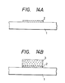
- Figs. 14A and 14B illustrate schematically the selective deposition method.
- a thin film 2 comprising a material different in the above factors from the substrate 1 is formed at a desired portion.
- a thin film 3 comprising an appropriate material is performed on the surface of the thin film 2 according to appropriate deposition conditions, it becomes possible to cause a phenomenon to occur such that the thin film 3 will grow only on the thin film 2 without growth on the substrate 1.
- the present invention utilizes the aforementioned difference of nucleation density, and is to form a nucleation surface with a different material having a sufficiently larger nucleation density than the material constituting a nonnucleation surface sufficiently finely to such an extent as to allow only a single nucleus to grow thereon, thereby performing the selective growth of a monocrystal only on the fine nucleation surface from the single nucleus formed thereon.
- the materials which can be utilized in the present invention there may be included, for example, SiO x (0 ⁇ x ⁇ 2) as the material of nonnucleation surface, Si, GaAs, silicon nitride as the materials of nucleation surface, and Si, W, GaAs, InP, etc. as the monocrystalline materials to be allowed to grow.
- the present invention is not limited by these materials, but the nucleation density difference may be sufficiently 102-fold or more in terms of the density of nucleus, and sufficient selective formation of a monocrystalline deposited film can be performed with the materials as exemplified below.
- a region containing excessively Si, N, etc. may be also formed by ion implantation of Si, N, etc. locally on the SiO2 film.
- nucleation surface with lower nucleation density e.g. SiO2
- SiO2 the material forming nucleation surface with lower nucleation density
- the selective monocrystal forming method as described above is practiced in liquid phase containing materials for formation of monocrystals, a solution containing a depositing material for preparing monocrystal dissolved in an appropriate solvent is prepared. The substrate for formation of monocrystals is then dipped into said solution super-saturated with the depositing material.
- Si is the depositing material
- Ga, In, Sb, Bi, Sn, etc. is used as the above solvent.
- Fig. 1 is a schematic constitutional view showing an example of the device to be used for practicing the selective monocrystal forming method in liquid phase of the present invention.
- 31 is a substrate to allow selective monocrystal formation on its surface, and said substrate 31 is held by fixing with a substrate holder 32, and said substrate holder 32 is suspended from above by a substrate supporting rod 33.
- 34 is a crucible and the above solution 35 is housed in said crucible.
- the above members are arranged in the treatment chamber 36, and a heater 37 is arranged around said treatment chamber.
- the treatment chamber 36 is internally heated to an appropriate temperature with the heater 37 and gradually cooled at an appropriate speed.
- selective formation of monocrystals is gradually performed while continuing the state of the solution 35 super-saturated with the depositing material.
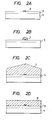
- Figs. 2A - 2D illustrate diagramatically the steps for illustration of the first embodiment of the method for forming crystals according to the present invention
- Figs. 3A and 3B are perspective views of Figs. 2A and 2D.
- a nonnucleation surface 5 with small nucleation density is formed, and a material with larger nucleation density is thinly deposited thereon, followed by patterning by lithography, etc. to form a nucleation surface 6 sufficiently finely such that only a single nucleus may be formed to obtain a substrate for crystal formation.
- the size, the crystal structure and the composition of the substrate 4 may be as desired, and it may be a substrate having a functional device formed thereon.
- the nucleation surface 6 is inclusive of modified regions having excessively Si, N, etc. formed by ion implantation of Si, N, etc. on the thin film 5, as described above.
- the substrate 4 having the nonnucleation surface 5 and the nucleation surface 6 is dipped into a solution containing a material for crystal formation as a crystal forming treatment, thereby forming a single nucleus on the nucleation surface 5 to allow a monocrystal to grow from the single nucleus.
- the above crystal forming treatment is carried out using a device for liquid-phase growth as shown in Fig. 1, and the substrate for crystal formation mentioned above is dipped into a solution comprising the mixture of a metal solvent and a solute of crystal forming material while the solution temperature is controlled to keep the supersaturated state of the solute, thereby depositing a monocrystal on the nucleation surface.
- a solution comprising the mixture of a metal solvent and a solute of crystal forming material while the solution temperature is controlled to keep the supersaturated state of the solute, thereby depositing a monocrystal on the nucleation surface.
- Si monocrystalline wafer is used as the substrate 4 and the nonnucleation surface 5 comprising SiO2 amorphous film is formed by thermal oxidation of the surface of said wafer.
- a quartz substrate may be employed, or alternatively SiO2 layer may be formed as the nonnucleation surface on the surface of any desired substrate such as metal, semiconductor, magnetic material, piezoelectric material, insulator, etc. by use of the sputtering method, the CVD method, the vaccum vapor deposition method, etc.
- SiO2 is desirable, but SiO x (0 ⁇ x ⁇ 2) with various x values may be also employed.
- a silicon nitride layer (here Si3N4 layer) is deposited by the reduced pressure vapor deposition method, followed by patterning of the silicon nitride layer according to conventional lithographic technique to form finely the nucleation surface 6 of preferably 10 ⁇ m or less in area, more preferably 5 ⁇ m or less, most preferably 1 ⁇ m or less, thus giving a substrate.
- the substrate is dipped into the solution containing materials for formation of crystals and performed the treatment for formation of crystals, subsequently, only a single nucleus is formed on the nucleation surface 6.
- the single nucleus grows while maintaining a monocrystalline structure to become a monocrystalline grain 7 shaped in an island as shown in Fig. 2B.
- the island-shaped monocrystalline grain 7 further grows while maintaining the monocrystalline structure with the nucleation surface 6 as the center, whereby the nonnucleation surface 5 becomes wholly covered therewith as shown in Fig. 2C.
- the surface of the monocrystalline grain 7 is flattened by etching or polishing to form a monocrystalline layer 8 on which a desired device can be formed, as shown in Fig. 2D and Fig. 3B.
- any desired material can be used for the substrate 4 which becomes the supporting member. Further, even if the substrate 4 may be one having a functional device, etc. formed thereon, a monocrystalline layer can be easily formed thereon.
- the so-called “melt-back phenomenon”, i.e. dissolution of the portion of monocrystalline substrate material itself contacting with the solution, which has been a problem involved in the conventional selective epitaxial growth (SEG) using a monocrystal and SiO2, etc. does not come into a problem since the nucleation surface 6 comprising silicon nitride and silicon oxide formed by ion implantation of Si, N, etc.
- deposition is effected under the conditions extremely close to thermal equilibrium with the degree of supersaturation of crystal material in the solution kept small, thus resulting in formation of a monocrystal of good quality containing no crystal defect, etc.
- a crystal of desired conduction type i.e. p-type, i-type or n-type
- relatively high level of doping can be performed in comparison with the crystal forming treatment in vapor phase.
- a Group III metal such as Ga, In, etc. may be used as a solvent for forming a p-type crystal to thereby enhance the carrier density as the following.
- a Group V metal such as Sb, Bi, etc. may be used as a solvent for forming an n-type crystal to thereby enhance the carrier density as the following.
- a Group IV metal may be used as a solvent for forming an i-type crystal to thereby obtaining the carrier density as the following.
- any appropriate desired impurity can be added later to the crystal obtained, and a crystal determined in conductive type is formed with desired doping concentration.
- the crystal forming surface is formed of a thin film, but of course as shown in Figs. 4A - 4D, the monocrystalline layer may be formed similarly by using the substrate comprising a material with small nucleation density enabling selective monocrystal growth as such.
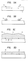
- Figs. 4A - 4D illustrate diagramatically the second embodiment of the present invention.
- a nucleation surface 6 sufficiently finely on the substrate 9 comprising a material with small nucleation density enabling selective nucleation, a monocrystalline layer 8 can be formed similarly as in the first embodiment.
- Figs. 5A - 5D illustrate diagramatically the third embodiment of the method of forming crystals according to the present invention
- Figs. 6A and 6B are perspective views in Figs. 5A and 5D.
- the nucleation surface 12 is arranged on the amorphous insulating substrate 11 sufficiently small with a distance l from each other.
- the distance l is set equal to or greater than the size of the monocrystalline region required for formation of a semiconductor device.
- nucleation surface 12 is required to be formed sufficiently finely to the extent that only a single nucleus may be formed.
- the size of the nucleation surface 12, which may differ depending on the kind of the material, may be within the above range.
- the crystal orientation in the direction of the island-shaped monocrystalline grain 13 normal to the substrate is determined constant so as to make the interfacial energy between the material of substrate 11 and the thin film depositing material minimum.
- the surface or interfacial energy has anisotropy depending on the crystal face.
- the island-shaped monocrystalline grain 13 further grows to contact the adjacent monocrystalline grain 13 as shown in Fig. 5C, and a crystal grain boundary 14 is formed almost at the intermediate position of the nucleation surface 12.
- the monocrystalline grain 13 grows three-dimensionally, but since the crystal face with slow growth speed appears as facet, the surface is flattened by etching or polishing, and further the portion of the grain boundary 14 is removed to form a thin film 15 of monocrystal containing no grain boundary in shape of a lattice as shown in Fig. 5D and Fig. 6B.
- the size of the monocrystalline thin film 15 is determined by the interval between the different materials 12 as described above. In other words, by determining the formed pattern of the different kind of material 12 appropriately, the position of the grain boundary can be controlled to form monocrystals with desired sizes at a desired arrangement.
- Figs. 7A - 7D illustrate diagramatically the steps showing the fourth embodiment of the present invention.
- a non-nucleation surface 5 comprising a material with small nucleation density enabling selective monocrystal growth is formed, and nucleation surface 12 is formed with intervals of l thereon, whereby a monocrystalline layer 15 can be formed similarly as in the above third embodiment.
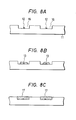
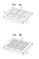
- Figs. 8A - 8C illustrate diagramatically the formation steps showing the fifth embodiment of the method of forming crystals according to the present invention
- Figs. 9A and 9B are perspective views in Figs. 8A and 8C.
- a concavity 16 with necessary size and shape is formed on the amorphous insulating substrate 11, and the nucleation surface 12 with fine size is formed therein.
- an island-shaped monocrystalline grain 13 is permitted to grow similarly as in the first embodiment.
- the monocrystalline grain 13 is permitted to grown until filling the concavity 16, thus forming a monocrystalline layer 17.
- Figs. 10A - 10C illustrate diagramatically the sixth embodiment of the present invention.
- a thin film 18 which becomes a nonnucleation surface comprising a material with small nucleation density enabling selective deposition is formed, and a concavity 16 with necessary size and shape is formed thereon.
- the nucleation surface 12 is formed finely therein, and a monocrystalline layer 17 is formed similarly as in the fifth embodiment.
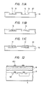
- Fig. 11A - 11C illustrate diagramatically the formation steps showing the seventh embodiment.
- a thin film 20 which becomes a nonnucleation surface comprising a material with small nucleation density enabling selective deposition is formed, and following the same procedure as described above, a monocrystalline layer 17 can be formed.
- Fig. 12 is a schematic sectional view showing an example of the multi-layer structure prepared by use of the first embodiment of the present invention.
- a transistor 101 or other semiconductor device or optical device, etc. is formed according to the conventional production process, and an SiO2 layer 5 as the non-nucleation surface is formed thereon according to the CVD method or the sputtering method. And, as already described, a monocrystal is permitted to grow on a sufficiently fine nucleation surface, thereby forming a monocrystalline layer 8.
- a transistor 102 or other semiconductor device or optical device is formed on the monocrystalline layer 8 and connected through the SiO2 layer 5.
- CMOS complementary metal-oxide-semiconductor
- its driving circuit can be integrated with an emitting device to accomplish high integration.
- monocrystalline layers 8 can be formed in many layers with SiO2 layer 5 sandwiched therebetween to form easily a multi-layer structure.
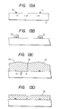
- Figs. 13A - 13D illustrate diagramatically the formation steps of the eighth embodiment of the present invention.
- Figs. 13A - 13C are the same as Figs. 5A - 5C. That is, the nucleation surface 12 is formed with interval l to form monocrystalline grain 13. By this, the grain boundary 14 is formed at substantially the center of the nucleation surface 12, and a polycrystalline layer 21 with a grain size l as shown in Fig. 13D can be obtained.
- the grain size of the polycrystalline layer 21 can be determined by the interval l between the nucleation surface 12, it becomes possible to control the grain size.
- the grain size of polycrystal was varied depending on a plural number of factors such as the formation method, the formation temperature, etc., but according to the present invention, it can be determined with good controllability by the interval l between the nucleation surface 12.
- the above polycrystalline layer 21 may be also formed by forming a depositing surface material layer 5 with small nucleation density on a desired substrate 4.
- the polycrystalline layer can be formed without restriction to the substrate, the material, etc. of the substrate.
- the material is not limited to Si3N4, but it may be also a silicon nitride with its composition being varied.
- the plasma CVD method in which a silicon nitride film is formed at low temperature by decomposing SiH4 gas and NH3 gas in RF plasma, by varying the flow rate ratio of SiH4 gas to NH3 gas, the composition ratio of Si to N in the silicon nitride film deposited can be varied to great extent.
- the substrate temperature at 380 °C and SiH4 gas flow rate is fixed at 300 cc/min.
- the gas flow rate ratio of NH3/SiH4 is varied from 4 to 10 by varying the flow rate of NH3 gas, it has been found by the Auger's electron spectroscopy that the Si/N ratio in the silicon nitride film is varied from 1.1 to 0.58.
- the composition of the silicon nitride film formed by introducing SiH2Cl2 gas and NH3 gas under the conditions of a reduced pressure of 0.3 Torr and a temperature of about 800 °C, was found to be approximately to Si3N4 (Si/N 0.75) which is the stoichiometric ratio.
- the silicon nitride film formed by the heat treatment of Si in ammonia or N2 at about 1200 °C can be obtained with a composition further approximate to the stoichiometric ratio, because its formation method is performed under thermal equilibrium.
- ion implanation of Si, N, P, B, F, Ar, He, C, As, Ga, Ge, etc. may be effected locally onto the surface of SiO2 which is the material with lower nucleation density to form a modified region on the non-nucleation surface, and the modified region may be utilized as the nucleation surface with higher nucleation density.
- the SiO2 surface is covered with a resist, and the desired sites are exposed to light, developed and dissolved to have the SiO2 surface partially exposed.
- SiF4 gas as the source gas, Si ions are implanted onto the SiO2 surface at 10 keV at a density of 1 ⁇ 1016 to 1 ⁇ 1018 cm ⁇ 2.
- the projected flight length is 114 ⁇ , and Si concentration reaches ca. 1022 cm ⁇ 3 on the SiO2 surface.
- SiO2 is amorphous, the region implanted with Si ions is also amorphous.
- ion implantation can be effected with a resist as the mask, but narrowed Si ions may be also implanted onto the SiO2 surface by use of the converging ion beam technique without use of the resist mask.
- a single nucleus of Si can be grown with the modified region as the nucleation surface whereby a single crystal can be grown as described above.
- Formation of the modified region sufficiently finely to the extent that a single nucleus can be grown can be accomplished by patterning of the resist or narrowing the beam of the converging ion beam.
- the whole surface may be once formed with a nucleation surface forming material, then a layer of non-nucleation surface forming material such as SiO2, etc. formed on said nucleation surface forming material, and a fine window opened by etching at a desired portion of said non-nucleation surface forming material layer, to have the nucleation surface exposed as fine region from said window.
- a nucleation surface forming material and the non-nucleation surface forming material the same as those described above can be used.
- GaAs crystals can be formed. More specifically, a nucleation surface is formed by ion implantation of Ga ions, As ions, Si ions, etc. at 1 ⁇ 1015 cm ⁇ 2 or higher in the fine regions on the SiO2 surface. Alternatively, a silicon nitride film may be formed in fine regions of the SiO2 surface, and its surface may be made the nucleation surface.
- Ga is employed as the solvent, and cooling is carried out at a temperature of 700 to 800 °C at a rate of 0.15 to 0.2 °C/min., growth of GaAs crystals occurs.
- InGaAs crystals can be formed. More specifically, a nucleation surface is formed by ion implantation of In ions, Ga ions, As ions, etc. in fine regions of the SiO2 surface at 1 ⁇ 1015 cm ⁇ 2 or more. Alternatively, a silicon nitride film may be formed in fine regions of the SiO2 surface, and its surface may be utilized as the nucleation surface.
- Ga is used as the solvent, and cooling is carried out at a temperature of 500 to 600 °C at a rate of 0.1 to 0.3 °C/min., InGaAs crystals will grow.
- the base substrate may be a substrate of a material capable of forming the above material layer, which becomes non-nucleation surface whereby the scope of selection can be broadened to great extent, whereby lowered cost and enlarged area can be accomplished with ease.
- the combinations of the material constituting a non-nucleation surface, the material constituting a nucleation surfaces and the crystalline material as described above are not limited to those shown in the above embodiments, but combinations of materials having sufficient nucleation density difference are clearly available. Therefore, also in the case of compound semiconductors such as InP, etc. capable of growth, monocrystals, monocrystal groups or polycrystals controlled in grain size can be formed.
- the above Si3N4 layer was patterned by the lithography technique to form fine Si3N4 regions as nucleation surfaces arranged in a matrix of 1 ⁇ m size, 150 ⁇ m pitch and 50 ⁇ 100 arrangement (as shown in Fig. 5A and Fig. 6A).
- Si monocrystals were formed by liquid phase crystal forming treatment under the following Si monocrystal forming conditions.
- Solvent Sn Solute: Si (saturation amount at 900 °C) Growth temperature: 900 °C - 864 °C Cooling rate: 0.4 °C/min Time: 1.5 hrs
- the Si monocrystal wafer subjected to crystal forming treatment was taken out of the device, and the crystal evaluation was performed by electronmicroscope observation and X-ray diffraction. As a result, it was found that 50 ⁇ 100 Si monocrystals having a grain size of 80 ⁇ m with an extremely narrow distribution were formed. It was also found that these Si monocrystals all had excellent monocrystalinity.
- An Si polycrystal was formed under similar conditions to Example 1.
- the surface of the polycrystal layer was subjected to flattening treatment by the selective etching technique employed conventionally in the art of semiconductor.
- a p MOS transistor was fabricated according to the method used conventionally in the art of semiconductor, and the operation characteristics thereof were investigated. As a result, it was found that the characteristics were remarkably excellent as compared to a p MOS transistor fabricated by using an Si polycrystal layer obtained by the conventional method.
- the crystals and the method of producing the same by forming on a substrate surface a nucleation surface forming material with sufficiently greater nucleation density than the material of said surface portion sufficiently finely so that a single nucleus may grow, permit a monocrystal from said nucleation surface with said substrate surface as the nonnucleation surface and the surface comprising the different kind of material as the nucleation surface, whereby crystals such as monocrystals with necessary sizes, a plural number of island-shaped monocrystals and polycrystals controlled in grain size, etc. can be easily formed on the base substrate. Moreover, they can be formed by use of a device conventionally used in semiconductor process without requiring a special production device.
- the crystals of the present invention are not restricted in the materials for the base substrate, and therefore three-dimensional integration, enlargement of area and lowered cost can be easily accomplished.
- monocrystals or polycrystals of silicon which are primary materials of semiconductor devices can be easily formed on an amorphous insulating material, multi-layer formation of devices with excellent electrical characteristics can be accomplished to realize a multi-functional integrated circuit not found in the prior art.
- integration of optical device, surface acoustic device, piezoelectric device, etc. or integration of each thereof with surrounding circuit C, etc. can be realized.
- inexpensive glass or ceramics, etc is used as the substrate material, application to a large area electronic device such as large scale flat panel display, etc. with the driving circuit integrated in one sheet of glass, etc. will become possible.
- the present invention by forming the above nucleation surface forming materials with desired distance on the deposited surface, can form monocrystals with necessary sizes on a plurality of sites, whereby the formation steps can be simplified to great extent and also the formation time shortened as compared with the melting and solidification method which forms monocrystals by irradiation of laser or electron beam.
- a polycrystal with grain sizes controlled by the interval can be formed.
- the method of forming polycrystals has better controllability in grain size and also the forming speed is shortened to great extent, as compared with the prior art method in which polycrystals with large grain sizes are formed according to the above melting and solidification method.
Landscapes
- Chemical & Material Sciences (AREA)
- Engineering & Computer Science (AREA)
- Crystallography & Structural Chemistry (AREA)
- Materials Engineering (AREA)
- Metallurgy (AREA)
- Organic Chemistry (AREA)
- Recrystallisation Techniques (AREA)
Applications Claiming Priority (2)
| Application Number | Priority Date | Filing Date | Title |
|---|---|---|---|
| JP73605/87 | 1987-03-27 | ||
| JP7360587 | 1987-03-27 |
Publications (2)
| Publication Number | Publication Date |
|---|---|
| EP0284434A2 true EP0284434A2 (fr) | 1988-09-28 |
| EP0284434A3 EP0284434A3 (fr) | 1989-03-22 |
Family
ID=13523129
Family Applications (1)
| Application Number | Title | Priority Date | Filing Date |
|---|---|---|---|
| EP88302718A Withdrawn EP0284434A3 (fr) | 1987-03-27 | 1988-03-25 | Procédé de préparation de cristaux |
Country Status (2)
| Country | Link |
|---|---|
| EP (1) | EP0284434A3 (fr) |
| CA (1) | CA1333248C (fr) |
Cited By (5)
| Publication number | Priority date | Publication date | Assignee | Title |
|---|---|---|---|---|
| DE4134261A1 (de) * | 1990-10-16 | 1992-05-07 | Canon Kk | Verfahren zur herstellung von halbleiterschichten und photovoltaischen einrichtungen |
| DE10117306A1 (de) * | 2001-04-02 | 2002-10-17 | Forschungsverbund Berlin Ev | Verfahren zur Herstellung einer strukturierten Dünnschicht-Anordnung |
| WO2012106071A1 (fr) * | 2011-01-31 | 2012-08-09 | Corning Incorporated | Article et procédé pour la formation de couches de silicium polycristallin à gros grains |
| WO2014001886A1 (fr) * | 2012-06-27 | 2014-01-03 | Rgs Development B.V. | Film de matériau semi-conducteur polycristallin, procédé de fabrication de celui-ci et moules d'orientation/surfusion pour celui-ci, et dispositif électronique |
| WO2014001888A1 (fr) * | 2012-06-27 | 2014-01-03 | Rgs Development B.V. | Film de matériau semi-conducteur polycristallin, procédé de fabrication de celui-ci et moules de surfusion pour celui-ci, et dispositif électronique |
Family Cites Families (4)
| Publication number | Priority date | Publication date | Assignee | Title |
|---|---|---|---|---|
| US4547230A (en) * | 1984-07-30 | 1985-10-15 | The United States Of America As Represented By The Secretary Of The Air Force | LPE Semiconductor material transfer method |
| US4657603A (en) * | 1984-10-10 | 1987-04-14 | Siemens Aktiengesellschaft | Method for the manufacture of gallium arsenide thin film solar cells |
| JPH0782996B2 (ja) * | 1986-03-28 | 1995-09-06 | キヤノン株式会社 | 結晶の形成方法 |
| EP0281335A3 (fr) * | 1987-02-28 | 1988-11-09 | Canon Kabushiki Kaisha | Procédé pour la fabrication d'un objet en semi-conducteur |
-
1988
- 1988-03-25 CA CA 562509 patent/CA1333248C/fr not_active Expired - Fee Related
- 1988-03-25 EP EP88302718A patent/EP0284434A3/fr not_active Withdrawn
Cited By (6)
| Publication number | Priority date | Publication date | Assignee | Title |
|---|---|---|---|---|
| DE4134261A1 (de) * | 1990-10-16 | 1992-05-07 | Canon Kk | Verfahren zur herstellung von halbleiterschichten und photovoltaischen einrichtungen |
| DE10117306A1 (de) * | 2001-04-02 | 2002-10-17 | Forschungsverbund Berlin Ev | Verfahren zur Herstellung einer strukturierten Dünnschicht-Anordnung |
| DE10117306B4 (de) * | 2001-04-02 | 2005-10-13 | Forschungsverbund Berlin E.V. | Verfahren zur Herstellung einer strukturierten Dünnschicht-Anordnung |
| WO2012106071A1 (fr) * | 2011-01-31 | 2012-08-09 | Corning Incorporated | Article et procédé pour la formation de couches de silicium polycristallin à gros grains |
| WO2014001886A1 (fr) * | 2012-06-27 | 2014-01-03 | Rgs Development B.V. | Film de matériau semi-conducteur polycristallin, procédé de fabrication de celui-ci et moules d'orientation/surfusion pour celui-ci, et dispositif électronique |
| WO2014001888A1 (fr) * | 2012-06-27 | 2014-01-03 | Rgs Development B.V. | Film de matériau semi-conducteur polycristallin, procédé de fabrication de celui-ci et moules de surfusion pour celui-ci, et dispositif électronique |
Also Published As
| Publication number | Publication date |
|---|---|
| EP0284434A3 (fr) | 1989-03-22 |
| CA1333248C (fr) | 1994-11-29 |
Similar Documents
| Publication | Publication Date | Title |
|---|---|---|
| US5281283A (en) | Group III-V compound crystal article using selective epitaxial growth | |
| EP0244081B1 (fr) | Méthode de fabrication d'un cristal et article cristallin obtenu par cette méthode | |
| US5130103A (en) | Method for forming semiconductor crystal and semiconductor crystal article obtained by said method | |
| JPH0766922B2 (ja) | 半導体装置の製造方法 | |
| US5447117A (en) | Crystal article, method for producing the same and semiconductor device utilizing the same | |
| JP2596547B2 (ja) | 太陽電池及びその製造方法 | |
| EP0277415A2 (fr) | Dispositif semi-conducteur utilisant une structure d'isolation et procédé pour sa fabrication | |
| EP0281335A2 (fr) | Procédé pour la fabrication d'un objet en semi-conducteur | |
| EP0240309B1 (fr) | Méthode de fabrication d'un cristal et cristal ainsi produit | |
| AU651568B2 (en) | Method for forming crystalline deposited film | |
| US5653802A (en) | Method for forming crystal | |
| US5254211A (en) | Method for forming crystals | |
| CA1333248C (fr) | Methode de formation de cristaux | |
| JPH03132016A (ja) | 結晶の形成方法 | |
| CA1329756C (fr) | Methode de formation d'un depot cristallin | |
| US5190613A (en) | Method for forming crystals | |
| EP0284437A2 (fr) | Article en cristal III-V et son procédé de fabrication | |
| US5118365A (en) | Ii-iv group compound crystal article and process for producing same | |
| JP2756320B2 (ja) | 結晶の形成方法 | |
| Tillack et al. | Thick monocrystalline silicon on oxidized silicon wafers produced by a zone melting process using a scanning halogen lamp | |
| JP2592834B2 (ja) | 結晶物品およびその形成方法 | |
| JP2659745B2 (ja) | ▲iii▼−v族化合物結晶物品およびその形成方法 | |
| EP0289117B1 (fr) | Procédé de préparation de cristaux sur un substrat | |
| JP2659746B2 (ja) | ▲ii▼−▲vi▼族化合物結晶物品およびその形成方法 | |
| EP0289114B1 (fr) | Procédé pour la production de cristaux sur un substrat transparent à la lumière |
Legal Events
| Date | Code | Title | Description |
|---|---|---|---|
| PUAI | Public reference made under article 153(3) epc to a published international application that has entered the european phase |
Free format text: ORIGINAL CODE: 0009012 |
|
| AK | Designated contracting states |
Kind code of ref document: A2 Designated state(s): DE FR GB IT NL |
|
| PUAL | Search report despatched |
Free format text: ORIGINAL CODE: 0009013 |
|
| RHK1 | Main classification (correction) |
Ipc: H01L 21/20 |
|
| AK | Designated contracting states |
Kind code of ref document: A3 Designated state(s): DE FR GB IT NL |
|
| 17P | Request for examination filed |
Effective date: 19890809 |
|
| 17Q | First examination report despatched |
Effective date: 19910718 |
|
| STAA | Information on the status of an ep patent application or granted ep patent |
Free format text: STATUS: THE APPLICATION IS DEEMED TO BE WITHDRAWN |
|
| 18D | Application deemed to be withdrawn |
Effective date: 19980425 |