EP0285168A2 - Supraleitender Draht und Verfahren zu seiner Herstellung - Google Patents
Supraleitender Draht und Verfahren zu seiner Herstellung Download PDFInfo
- Publication number
- EP0285168A2 EP0285168A2 EP88105293A EP88105293A EP0285168A2 EP 0285168 A2 EP0285168 A2 EP 0285168A2 EP 88105293 A EP88105293 A EP 88105293A EP 88105293 A EP88105293 A EP 88105293A EP 0285168 A2 EP0285168 A2 EP 0285168A2
- Authority
- EP
- European Patent Office
- Prior art keywords
- melt
- solidifying
- group
- element selected
- cooling
- Prior art date
- Legal status (The legal status is an assumption and is not a legal conclusion. Google has not performed a legal analysis and makes no representation as to the accuracy of the status listed.)
- Granted
Links
Images

Classifications
-
- H—ELECTRICITY
- H10—SEMICONDUCTOR DEVICES; ELECTRIC SOLID-STATE DEVICES NOT OTHERWISE PROVIDED FOR
- H10N—ELECTRIC SOLID-STATE DEVICES NOT OTHERWISE PROVIDED FOR
- H10N60/00—Superconducting devices
- H10N60/01—Manufacture or treatment
- H10N60/0268—Manufacture or treatment of devices comprising copper oxide
- H10N60/0801—Manufacture or treatment of filaments or composite wires
-
- Y—GENERAL TAGGING OF NEW TECHNOLOGICAL DEVELOPMENTS; GENERAL TAGGING OF CROSS-SECTIONAL TECHNOLOGIES SPANNING OVER SEVERAL SECTIONS OF THE IPC; TECHNICAL SUBJECTS COVERED BY FORMER USPC CROSS-REFERENCE ART COLLECTIONS [XRACs] AND DIGESTS
- Y10—TECHNICAL SUBJECTS COVERED BY FORMER USPC
- Y10S—TECHNICAL SUBJECTS COVERED BY FORMER USPC CROSS-REFERENCE ART COLLECTIONS [XRACs] AND DIGESTS
- Y10S505/00—Superconductor technology: apparatus, material, process
- Y10S505/70—High TC, above 30 k, superconducting device, article, or structured stock
- Y10S505/704—Wire, fiber, or cable
-
- Y—GENERAL TAGGING OF NEW TECHNOLOGICAL DEVELOPMENTS; GENERAL TAGGING OF CROSS-SECTIONAL TECHNOLOGIES SPANNING OVER SEVERAL SECTIONS OF THE IPC; TECHNICAL SUBJECTS COVERED BY FORMER USPC CROSS-REFERENCE ART COLLECTIONS [XRACs] AND DIGESTS
- Y10—TECHNICAL SUBJECTS COVERED BY FORMER USPC
- Y10S—TECHNICAL SUBJECTS COVERED BY FORMER USPC CROSS-REFERENCE ART COLLECTIONS [XRACs] AND DIGESTS
- Y10S505/00—Superconductor technology: apparatus, material, process
- Y10S505/725—Process of making or treating high tc, above 30 k, superconducting shaped material, article, or device
- Y10S505/733—Rapid solidification, e.g. quenching, gas-atomizing, melt-spinning, roller-quenching
-
- Y—GENERAL TAGGING OF NEW TECHNOLOGICAL DEVELOPMENTS; GENERAL TAGGING OF CROSS-SECTIONAL TECHNOLOGIES SPANNING OVER SEVERAL SECTIONS OF THE IPC; TECHNICAL SUBJECTS COVERED BY FORMER USPC CROSS-REFERENCE ART COLLECTIONS [XRACs] AND DIGESTS
- Y10—TECHNICAL SUBJECTS COVERED BY FORMER USPC
- Y10S—TECHNICAL SUBJECTS COVERED BY FORMER USPC CROSS-REFERENCE ART COLLECTIONS [XRACs] AND DIGESTS
- Y10S505/00—Superconductor technology: apparatus, material, process
- Y10S505/725—Process of making or treating high tc, above 30 k, superconducting shaped material, article, or device
- Y10S505/739—Molding, coating, shaping, or casting of superconducting material
- Y10S505/74—To form wire or fiber
-
- Y—GENERAL TAGGING OF NEW TECHNOLOGICAL DEVELOPMENTS; GENERAL TAGGING OF CROSS-SECTIONAL TECHNOLOGIES SPANNING OVER SEVERAL SECTIONS OF THE IPC; TECHNICAL SUBJECTS COVERED BY FORMER USPC CROSS-REFERENCE ART COLLECTIONS [XRACs] AND DIGESTS
- Y10—TECHNICAL SUBJECTS COVERED BY FORMER USPC
- Y10T—TECHNICAL SUBJECTS COVERED BY FORMER US CLASSIFICATION
- Y10T29/00—Metal working
- Y10T29/49—Method of mechanical manufacture
- Y10T29/49002—Electrical device making
- Y10T29/49014—Superconductor
Definitions
- the present invention relates to a method of manufacturing a superconducting wire, and more particularly, it relates to a method of manufacturing a superconducting wire of a ceramics superconductive material.
- a wire rod of a ceramics superconductor is manufactured by:
- a raw material for the ceramics superconductor is generally filled in a metal pipe to be heated to a high temperature and thereafter extruded into the form of a wire rod, to be further subjected to wire drawing by a die or the like, if necessary.
- the raw material for the ceramics superconductor is subjected to heat treatment in a state isolated from the external atmosphere by the metal pipe, with insufficient reaction to elements required for the superconductor, such as oxygen.
- the superconductor cannot be provided with expected critical temperature and critical current. Further, the degree of fineness of the wire rod is restricted.
- Ceramics superconductive materials are recently being watched as the same can be increased in critical temperature of superconduction.
- Such superconductive materials can be shaped into elongated linear bodies, for example, to be applied to uses such as power transmission/distribution, electric connection of various devices or elements, winding for a coil, and the like.
- An object of the present invention is to provide a method of efficiently manufacturing a superconducting wire of a ceramics superconductive material composed in design, which can be increased in critical temperature and worked into a wire rod with no degradation in electrical property, and a superconducting fine wire obtained by the said method.
- the present invention provides a method of manufacturing a superconductor made of a ceramics superconductive material, preferably a compound material containing oxygen and at least two sorts of metal elements and being in layer structure.
- A represents at least a single sort of element, preferably at least two sorts of elements selected from a group of those belonging to the groups Ia, IIa and IIIa of the periodic table.
- the elements belonging to the group Ia of the periodic table are H, Li, Na, K, Rb, Cs and Fr.
- the elements belonging to the group IIa of the periodic table are Be, Mg, Ca, Sr, Ba and Ra.
- the elements belonging to the group IIIa of the periodic table are Sc, Y, La, Ce, Pr, Nd, Pm, Sm, Eu, Gd, Tb, Dy, Ho, Er, Tm, Yb, Ly, Ac, Th, Pa, U, Np, Pu, Am, Cm, Bk, Cf, Es, Fm, Md, No and Lr.
- B in the general formula represents at least a single sort of element selected from a group of those belonging to the groups Ib, IIb and IIIb of the periodic table.
- the elements belonging to the group Ib of the periodic table are Cu, Ag and Au and those belonging to the group IIb are Zn, Cd and Hg, while those belonging to the group IIIb are B, Al, Ga, In and Tl.
- C represents at least a single sort of element selected from a group of oxygen, carbon, nitrogen, fluorine and sulfur.
- B preferably contains at least copper and C preferably contains at least oxygen, for the possibility of attaining a higher critical temperature.
- first prepared is a raw material composed of a compound containing oxygen and at least two sorts of metal elements and being in layer structure, or a raw material being in composition generally expressed in the formula AaBbCc.
- the raw material is molten in a vessel having a hole provided to communicate with its interior.
- a melt obtained by such melting is linearly discharged from the hole by either extrusion or drawout.
- the linearly discharged melt is cooled and solidified.
- This melt may be solidified by forced cooling or natural standing.
- at least a sort of vitrifying compound such as B2O3, GeO2 or P2O5 may be added in the step of melting the raw material, in order to bring the melt into a highly viscous glassy state. In this case, the solidified body as obtained may be crystallized by further re-heating.
- the ceramics superconductive material can be brought into a considerably viscous state through melting in a heating vessel.
- a superconducting wire rod can be obtained by extruding or drawing out the melt from the hole. Since the melt is extruded or drawn out in the considerably viscous state, the wire rod can be extremely reduced in thickness along the size of the hole.
- a superconducting wire rod is manufactured by melting a ceramics superconductive material and extruding or drawing out the same, whereby a superconducting wire rod having a high critical temperature and excellent electrical properties can be obtained by a simple method.
- a ceramics superconducting wire being composed in design even if the raw material is correctly prepared in composition.
- the composition of the ceramics superconducting wire is easily fluctuated by dissociation or coupling of elements contained in the raw material being in a molten state.
- the inventors have found out that a ceramics superconducting wire can be reliably composed in design by adjusting an atmosphere at least in one of the entire steps including melting and cooling/solidifying steps.
- a raw material being in composition generally expressed in a formula AaBbC x c x in manufacturing of a ceramics superconductor of the aforementioned composition.
- C x represents at least a single sort of element selected from a group of oxygen, carbon, nitrogen and sulfur, which may be identical to the aforementioned element C or a part of C if C consists of two or more elements.
- the general c x represents a number showing the composition ratio of C x .
- the material expressed as AaBbC x c x is first prepared to be molten.
- the method further comprises at least a step of linearly discharging a melt of AaBbC x c x obtained by melting through extrusion or drawout and a step of cooling and solidifying the linearly discharged melt of AaBbC x c x .
- This manufacturing method may comprise at least the melting step, the discharging step and the cooling/solidifying step, and hence some steps may be freely performed after the melt is solidified.
- the inventive manufacturing method is characterized in that at least one of the entire steps including the aforementioned melting, discharging and cooling/solidifying steps is performed under an atmosphere containing a C y component of partial pressure being higher than C y partial pressure in the atmospheric air.
- the C y component is prepared by a gas containing at least a single sort of element selected from a group of oxygen, nitrogen, carbon, fluorine and sulfur.
- C y may be identical to C in the aforementioned final composition expressed in the general formula AaBbCc, while the same at least contains difference between C and C x , i.e., an element left by eliminating C x from C if C consists of two or more elements.
- Examples of the C y gas are oxygen, nitrogen, carbon monoxide, carbon dioxide, hydrogen fluoride and hydrogen sulfide.
- the aforementioned atmosphere in which C y partial pressure is higher than that in the atmospheric air may be introduced into "at least" one of the entire steps.
- only the melting step may be performed under the said atmosphere, while only the cooling/solidifying step may alternatively be performed under the said atmosphere.
- the melting step or the cooling/solidifying step is so performed under this atmosphere that melting or cooling/solidification is carried out in an atmosphere being rich in C y . Therefore, if C x is smaller in sort or amount of elements than C in the final composition, C y can be added to the material being in a molten or cooled state from the C y atmosphere, thereby to reliably attain Cc in the final composition.
- C x contained in the material is identical to C in the final composition, on the other hand, C y is prepared to be identical in element to C x and C thereby to suppress dissociation of the C component in the material being in a molten state or a state directed to solidification, or recombine the same upon dissociation.
- the material may be re-heated after the cooling/solidifying step under an atmosphere in which C y partial pressure is higher than that in the atmospheric air.
- C in the final composition can be attained by supplying the C y component in the re-heating step.
- the material expressed in the aforementioned general formula AaBbC x c x can be prepared by a partially fabricated item which is not completely superconductive, in addition to a mixed body and a compact.
- an element which is easily dissociated or changed in a molten state can be prevented from such dissociation or change by adjusting an atmosphere introduced into a part of the manufacturing steps, while an element not contained in the raw material can be supplied from the aforementioned atmosphere as the case may be.
- a ceramics superconducting wire can be reliably composed in design.
- inventive manufacturing method is applicable to a method of manufacturing a ceramics superconducting wire which is employed for general application of such a superconducting wire, in addition to that employed in the field of energy such as a high current density magnet or a long-distance transmission line or an electronic device such as a Josephson device.
- the present invention is further directed to a method of manufacturing a superconducting wire comprising the steps of melting a ceramics superconductive material in a vessel heated to a temperature exceeding the melting point thereof and extruding or drawing out the molten superconductive material from a hole communicating with the interior of the vessel to cool/solidify the same.
- This method is characterized in that the cooling/solidifying step is performed in a space being at a temperature between the solidifying point of the superconductive material and a temperature lower by 100°C than the solidifying point.
- a ceramics superconductive material being molten in a vessel is discharged from a hole communicating with the interior of the vessel to be cooled/solidified.
- the cooling/solidifying step is performed in an atmosphere of a temperature close to the solidifying point of the superconductive material, i.e., at a temperature level between the solidifying point and that lower by 100°C than the solidifying point, thereby to reduce thermal distortion caused in solidification of the molten superconductive material. Therefore, an elongated superconducting wire can be manufactured in high productivity with no breaking in or upon solidification of the molten ceramics superconductive material.
- the temperature of the space for performing the cooling/solidifying step is less than the temperature lower by 100°C than the solidifying point, an elongated superconducting wire cannot be readily obtained and the solidified superconducting wire is easily broken. It has been also confirmed by reduction in critical temperature that, if the said temperature is less than that lower by 100°C than the solidifying point as described above, the cooled/solidified ceramics material is not brought into desired perovskite or pseudo-perovskite structure, or the ratio of such crystal structure is reduced.
- the temperature of the space for carrying out the cooling/solidifying step is preferably selected to be closer to the solidifying point of the superconductive material, i.e., at a temperature level between the solidifying point and that lower by 50°C than the solidifying point in order to further reduce thermal distortion caused in solidification, thereby to further effectively manufacture an elongated superconducting wire of a ceramics superconductive material being in desired perovskite or pseudo-perovskite structure.
- a zone next to the space for performing the cooling/solidifying step is provided to be at a relatively high temperature in a portion closer to the hole of the vessel while having a temperature gradient along a direction for linearly discharging the melt, so that the cooled/solidified superconducting wire is passed through the zone to be slowly cooled.
- Desired perovskite or pseudo-peroskite structure can be further excellently attained in a superconducting wire thus obtained. This has been confirmed by measurement of a critical temperature.
- an average cooling rate is preferably selected to be not more than 10°C/min. at least until the temperature reaches 200°C.
- Fig. 1 is a process diagram schematically showing a method of manufacturing a superconducting wire according to the present invention.
- a raw material of prescribed composition is first prepared in the form of powder, a compact or the like. This raw material is molten in a vessel having a hole provided to communicate with its interior. A melt thus obtained is linearly discharged from the hole through extrusion or drawout. The linearly discharged melt is thereafter cooled to be solidified.
- a superconducting wire of prescribed composition is obtained in the form of a solidified body.
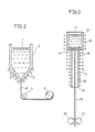
- Fig. 2 is a schematic block diagram showing an embodiment of a superconducting wire rod manufacturing apparatus for carrying out the present invention.
- a heating source 3 is provided in proximity to an extrusion port of a heating furnace 2 containing powder of a ceramics superconductive material 1. Further provided are a guide roll 4 for guiding a ceramics superconducting wire extruded through the extrusion port and a take-up roll 5 for winding the ceramics superconducting wire.
- powder of Y2O3, BaCO3 and CuO mixed in the ratio 0.2:0.6:1 was preliminarily sintered at 900°C for 10 hours and pulverized to prepare the ceramics superconductive material 1, which could be brought into a half-molten state by raising up the inner temperature of the heating furnace 2 to 1000°C by the heating source 3.
- the ceramics superconductive material 1 was extruded from the extrusion port to be wound on the take-up roll 5 through the guide roll 4, thereby to obtain a fine wire 6 of 100 ⁇ m in diameter.
- a superconducting magnet having a high critical temperature and excellent electrical properties can be implemented through the superconducting fine wire obtained in the aforementioned manner.
- a superconducting transmission cable having a high critical temperature and excellent electrical properties can be implemented through the superconducting fine wire.
- a stabilizing material such as copper is preferably adapted to hold or be held by a large number of fine wires, to prevent heat generation in quenching for transition into normal conduction as well as to prevent burning of the superconducting fine wires.
- the present invention is not restricted to the aforementioned Example but a ceramics superconducting material can be molten in a coarsely crushed state or the diameter of the wire rod can be set in a desired value other than 100 ⁇ m. Further, various modifications may be introduced in design within a scope of the present invention.
- a mixture of Y2O3, BaCO3 and CuO was molded and previously subjected to heat treatment, to be heated/molten in a crucible under an atmosphere containing oxygen of 200 Torr. Then the melt was drawn out from a nozzle of 500 ⁇ m in bore diameter, to be solidified in the form of a fine wire.
- the fine wire thus obtained was made of a ceramics superconductive material composed of Y 0.4 Ba 0.6 CuO 2.2 , which superconducted at 90 K.
- a material being in average composition of La 1.6 Sr 0.34 CuO4 containing 0.01 wt.% of fluorine was molten in a crucible under an atmosphere containing SF6 gas of 100 Torr., to manufacture a tape-like member of 30 ⁇ m in thickness and 60 mm in width similarly under an atmosphere containing SF6 gas of 100 Torr. by the so-called roll quenching method. This tape-like member superconducted at 40 K.
- Example 2 The material obtained in Example 2 was heated under an atmosphere containing oxygen of 200 Torr. at 1100°C for two hours, to obtain a ceramics superconductive material of Y 0.4 Ba 0.6 CuO 2.5 . This ceramics superconductive material superconducted at a temperature of 95 K.
- Fig. 3 illustrates a state of carrying out Example 5.
- a ceramics superconductive material 11 of YBa2Cu3O7 having a solidifying point of about 1090°C was molten at a temperature of 1180°C in a platinum crucible 13 heated by a heater 12.
- the molten ceramics superconductive material 11 was drawn out from a hole 14 provided on the bottom wall of the crucible 13 to be cooled/solidified, thereby to obtain a superconducting wire 15.
- the space for performing the aforementioned cooling/solidifying step was enclosed by a tunnel 16, for example, and provided with a prescribed temperature atmosphere by a heater 17 arranged in relation to the tunnel 16.
- the tunnel 16 was provided in its relatively upward portion with a cooling/solidifying space 18 being brought into a higher temperature atmosphere, while a slow-cooling zone 19 was formed in communication with the cooling/solidifying space 18.
- the cooling/solidifying space 18 was set at a temperature of 1080°C, while a lower end of the slow-cooling zone 19 was set at a temperature of 1050°C.
- the superconducting wire 15 discharged from the tunnel 16 was drawn out through a pair of rollers 20 and 21 rotated along arrows in Fig. 3.
- the superconducting wire 15 thus obtained was 50 ⁇ m in diameter, and superconducted at a critical temperature of 85 K.
- Reference example was prepared by the same superconducting wire 15 to draw out the same while stopping heating by the heater 17. However, the superconducting wire 15 was occasionally broken.
- a superconducting wire obtained by the inventive method is not restricted to that of a circular section.
- the sectional configuration of the superconducting wire depends on that of the hole 14 provided to communicate with the interior of the crucible 13, and a superconducting wire of an arbitrary sectional configuration, such as a tape-like one, can be obtained by changing the configuration of the hole 14.
- Respective powder materials of Bi2O3, SrCO3, CaCO3 and CuO were weighed so that Bi, Sr, Ca and Cu were in the composition ratio 1:1:1:2 and mixed with each other to be temporarily fired in the atmospheric air at 800°C for eight hours, thereby to prepare raw material powder to be molten.
- This powder was introduced into a crucible to be molten, drawn out and solidified in the atmospheric air through the apparatus as shown in Fig. 3, thereby to obtain a fine wire of 100 ⁇ m in diameter.
- This fine wire was annealed in the atmospheric air at 830°C for eight hours, and thereafter slowly cooled.
- the critical temperature T C of the fine wire thus obtained was measured through measurement of electric resistance by a general four-terminal method. This fine wire was in such superconductivity that its electric resistance reached zero at 100 K.
- a material obtained by adding B2O3 of 20 % in mole ratio to a ceramics superconductive material composed of Y1Ba2Cu3O 7-x was introduced into a crucible to be molten, drawn out and solidified in the atmospheric air at 800°C through the apparatus as shown in Fig. 3, thereby to obtain a fine wire of 50 ⁇ m in diameter This fine wire was in a partially crystallized glassy state. Then the fine wire was annealed in the atmospheric air at 700°C for six hours, and thereafter slowly cooled. The critical temperature T C of this fine wire was 85 K.
Landscapes
- Engineering & Computer Science (AREA)
- Manufacturing & Machinery (AREA)
- Superconductors And Manufacturing Methods Therefor (AREA)
- Compositions Of Oxide Ceramics (AREA)
- Inorganic Compounds Of Heavy Metals (AREA)
Applications Claiming Priority (6)
| Application Number | Priority Date | Filing Date | Title |
|---|---|---|---|
| JP8182087 | 1987-04-02 | ||
| JP81820/87 | 1987-04-02 | ||
| JP8656387 | 1987-04-07 | ||
| JP86563/87 | 1987-04-07 | ||
| JP9014787 | 1987-04-13 | ||
| JP90147/87 | 1987-04-13 |
Publications (3)
| Publication Number | Publication Date |
|---|---|
| EP0285168A2 true EP0285168A2 (de) | 1988-10-05 |
| EP0285168A3 EP0285168A3 (en) | 1990-08-08 |
| EP0285168B1 EP0285168B1 (de) | 1995-02-22 |
Family
ID=27303710
Family Applications (1)
| Application Number | Title | Priority Date | Filing Date |
|---|---|---|---|
| EP88105293A Expired - Lifetime EP0285168B1 (de) | 1987-04-02 | 1988-03-31 | Supraleitender Draht und Verfahren zu seiner Herstellung |
Country Status (4)
| Country | Link |
|---|---|
| US (1) | US4973574A (de) |
| EP (1) | EP0285168B1 (de) |
| CA (1) | CA1332026C (de) |
| DE (1) | DE3853089T2 (de) |
Cited By (8)
| Publication number | Priority date | Publication date | Assignee | Title |
|---|---|---|---|---|
| EP0369309A3 (en) * | 1988-11-15 | 1990-08-01 | Berkenhoff Gmbh | Process for producing high-temperature superconducting ductile composite materials, and composites produced by this process |
| EP0344813A3 (en) * | 1988-06-02 | 1990-08-08 | Sumitomo Electric Industries, Limited | Method of melting superconductive material |
| EP0369464A3 (en) * | 1988-11-18 | 1990-08-22 | Sumitomo Electric Industries, Limited | Method of producing superconducting ceramic wire |
| US4966886A (en) * | 1988-04-01 | 1990-10-30 | Junkosha Co., Ltd. | Superconducting cable with continuously porous insulation |
| US4970194A (en) * | 1989-07-21 | 1990-11-13 | Iowa State University Research Foundation | Method of producing superconducting fibers of YBA2CU30X |
| EP0445832A3 (de) * | 1990-03-08 | 1991-09-18 | Sumitomo Electric Industries, Ltd. | Verfahren zur Herstellung eines mit einer metallischen Schutzschicht versehenen supraleitenden Drahtes aus Keramik |
| US5229358A (en) * | 1989-06-15 | 1993-07-20 | Microelectronics And Computer Technology Corporation | Method and apparatus for fabricating superconducting wire |
| US5229357A (en) * | 1988-11-18 | 1993-07-20 | Sumitomo Electric Industries, Ltd. | Method of producing superconducting ceramic wire and product |
Families Citing this family (16)
| Publication number | Priority date | Publication date | Assignee | Title |
|---|---|---|---|---|
| CA1332513C (en) * | 1987-04-02 | 1994-10-18 | Yoshihiro Nakai | Superconductor and method of manufacturing the same |
| US5232909A (en) * | 1987-08-20 | 1993-08-03 | Sumitomo Electric Industries, Ltd. | Method for manufacturing superconducting ceramics elongated body |
| US5219831A (en) * | 1988-02-04 | 1993-06-15 | University Of Tokyo | Superconductive photoconductive-substance of the La-Cu-O system and a method for producing the same |
| US5077271A (en) * | 1988-12-02 | 1991-12-31 | Hewlett-Packard Company | Liquid phase epitaxial method for forming single crystal films of high temperature oxide superconductors |
| US5244871A (en) * | 1989-05-12 | 1993-09-14 | Mitsubishi Metal Corporation | N-type oxide superconductor represented by the formula (Ndx (Cey Lz)2 CuO4-d where L is La, Mg or a mixture of alakaline earth elements |
| US5053384A (en) * | 1989-07-21 | 1991-10-01 | Iowa State University Research Foundation, Inc. | Method of producing superconducting fibers of bismuth strontium calcium copper oxide (Bi(2212) and Bi(2223)) |
| FR2671425B1 (fr) * | 1991-01-04 | 1996-02-02 | Alsthom Cge Alcatel | Procede de fabrication d'un element du genre fil ou ruban en materiau a base d'oxyde supraconducteur a haute temperature critique et element ainsi obtenu. |
| US5219832A (en) * | 1991-06-18 | 1993-06-15 | Dawei Zhou | High-tc superconducting ceramic oxide products and macroscopic and microscopic methods of making the same |
| US5661114A (en) | 1993-04-01 | 1997-08-26 | American Superconductor Corporation | Process of annealing BSCCO-2223 superconductors |
| US6194352B1 (en) * | 1994-01-28 | 2001-02-27 | American Superconductor Corporation | Multifilament composite BSCCO oxide superconductor |
| US5660541A (en) * | 1994-10-13 | 1997-08-26 | General Atomics | Method for heat treating long lengths of silver clad high temperature superconductor |
| US5987342A (en) * | 1996-08-30 | 1999-11-16 | American Superconductor Corporation | Laminated superconducting ceramic tape |
| US6110606A (en) | 1996-08-30 | 2000-08-29 | American Superconductor Corporation | Cryogen protected superconducting ceramic tape |
| US6444917B1 (en) | 1999-07-23 | 2002-09-03 | American Superconductor Corporation | Encapsulated ceramic superconductors |
| US7704907B2 (en) * | 2005-08-25 | 2010-04-27 | Ceramext, Llc | Synthesized hybrid rock composition, method, and article formed by the method |
| CN113275379A (zh) * | 2021-06-02 | 2021-08-20 | 清远市进田企业有限公司 | 一种高延性电解铜制备工艺 |
Family Cites Families (6)
| Publication number | Priority date | Publication date | Assignee | Title |
|---|---|---|---|---|
| US3868241A (en) * | 1973-06-12 | 1975-02-25 | Combustion Eng | Manufacture of fused cast refractory with streams of oxygen |
| US4103063A (en) * | 1976-03-23 | 1978-07-25 | United Technologies Corporation | Ceramic-metallic eutectic structural material |
| US4104355A (en) * | 1976-05-03 | 1978-08-01 | Bjorksten Research Laboratories, Inc. | Vitreous fiber drawing process |
| JPS5474698A (en) * | 1977-11-28 | 1979-06-14 | Univ Tohoku | Superconductive thin band and method of fabricating same |
| EP0111728A3 (de) * | 1982-11-12 | 1985-04-03 | Concast Standard Ag | Verfahren und Vorrichtung zur Herstellung band- oder folienartiger Produkte |
| US4762754A (en) * | 1986-12-04 | 1988-08-09 | The United States Of America As Represented By The United States Department Of Energy | Dynamic high pressure process for fabricating superconducting and permanent magnetic materials |
-
1988
- 1988-03-31 CA CA000563080A patent/CA1332026C/en not_active Expired - Fee Related
- 1988-03-31 EP EP88105293A patent/EP0285168B1/de not_active Expired - Lifetime
- 1988-03-31 DE DE3853089T patent/DE3853089T2/de not_active Expired - Fee Related
- 1988-04-01 US US07/176,560 patent/US4973574A/en not_active Expired - Fee Related
Cited By (11)
| Publication number | Priority date | Publication date | Assignee | Title |
|---|---|---|---|---|
| US4966886A (en) * | 1988-04-01 | 1990-10-30 | Junkosha Co., Ltd. | Superconducting cable with continuously porous insulation |
| EP0344813A3 (en) * | 1988-06-02 | 1990-08-08 | Sumitomo Electric Industries, Limited | Method of melting superconductive material |
| US5643857A (en) * | 1988-06-02 | 1997-07-01 | Sumitomo Electric Industries, Ltd. | Method of melting ceramic superconductive material |
| EP0369309A3 (en) * | 1988-11-15 | 1990-08-01 | Berkenhoff Gmbh | Process for producing high-temperature superconducting ductile composite materials, and composites produced by this process |
| EP0369464A3 (en) * | 1988-11-18 | 1990-08-22 | Sumitomo Electric Industries, Limited | Method of producing superconducting ceramic wire |
| US4975416A (en) * | 1988-11-18 | 1990-12-04 | Sumitomo Electric Industries, Ltd. | Method of producing superconducting ceramic wire |
| US5229357A (en) * | 1988-11-18 | 1993-07-20 | Sumitomo Electric Industries, Ltd. | Method of producing superconducting ceramic wire and product |
| US5229358A (en) * | 1989-06-15 | 1993-07-20 | Microelectronics And Computer Technology Corporation | Method and apparatus for fabricating superconducting wire |
| US4970194A (en) * | 1989-07-21 | 1990-11-13 | Iowa State University Research Foundation | Method of producing superconducting fibers of YBA2CU30X |
| EP0445832A3 (de) * | 1990-03-08 | 1991-09-18 | Sumitomo Electric Industries, Ltd. | Verfahren zur Herstellung eines mit einer metallischen Schutzschicht versehenen supraleitenden Drahtes aus Keramik |
| US5232901A (en) * | 1990-03-08 | 1993-08-03 | Sumitomo Electric Industries, Inc. | Method of producing superconducting ceramic wire having protective metal coating thereon |
Also Published As
| Publication number | Publication date |
|---|---|
| EP0285168B1 (de) | 1995-02-22 |
| US4973574A (en) | 1990-11-27 |
| DE3853089T2 (de) | 1995-09-28 |
| DE3853089D1 (de) | 1995-03-30 |
| CA1332026C (en) | 1994-09-20 |
| EP0285168A3 (en) | 1990-08-08 |
Similar Documents
| Publication | Publication Date | Title |
|---|---|---|
| EP0285168B1 (de) | Supraleitender Draht und Verfahren zu seiner Herstellung | |
| Sandhage et al. | Critical issues in the OPIT processing of high-Jc BSCCO superconductors | |
| US5011823A (en) | Fabrication of oxide superconductors by melt growth method | |
| EP0505015B1 (de) | Supraleitender Draht und Verfahren zu seiner Herstellung | |
| EP0295023B1 (de) | Verfahren zur Herstellung eines supraleitenden Teiles und Anordnungen und Anlagen, die dieses Teil Aufweisen | |
| EP0281474B1 (de) | Verfahren zur Herstellung eines Oxid-Verbindungssupraleiterfadens | |
| EP0457851B1 (de) | Yttrium-barium-kupfer-sauerstoff-supraleiter mit gerichteten kristalliten und hoher kritischer stromdichte sowie verfahren zur ihrer herstellung | |
| US4857504A (en) | Melt-produced high temperature rare earth barium copper oxide superconductor and processes for making same | |
| EP0285169B1 (de) | Supraleiter und Verfahren zu seiner Herstellung | |
| JPH0494019A (ja) | ビスマス系酸化物超電導体の製造方法 | |
| EP0283024B1 (de) | Verfahren zur Herstellung eines keramischen Supraleiters | |
| US5206211A (en) | Process for the production of an elongate body consisting of longitudinally aligned acicular crystals of a superconducting material | |
| EP0304076B1 (de) | Verfahren zur Herstellung von supraleitenden Produkten | |
| US5217943A (en) | Process for making composite ceramic superconducting wires | |
| CA1330702C (en) | Method of producing long functional oxide objects | |
| US5401717A (en) | Elongate bismuth system superconductor having aligned 2212 phase | |
| KR930003843B1 (ko) | 초전도 물품의 제조방법 | |
| US5346883A (en) | Method of manufacturing superconductive products | |
| Poeppel et al. | Recent improvements in bulk properties of ceramic superconductors | |
| CA1338753C (en) | Method of producing oxide superconducting wire and oxide superconducting wire produced by this method | |
| JPH06187848A (ja) | 酸化物超伝導線材およびその製造方法 | |
| JPH02189817A (ja) | 酸化物超伝導テープ状線材の製造法 | |
| Goto | Partial-Melting of Filamentary Hg1223 Superconductors by Using CaHgO2 for the Vaporizing Material | |
| Hermann et al. | Process for making superconducting wires | |
| JPH087680A (ja) | 酸化物超伝導線材の製造方法 |
Legal Events
| Date | Code | Title | Description |
|---|---|---|---|
| PUAI | Public reference made under article 153(3) epc to a published international application that has entered the european phase |
Free format text: ORIGINAL CODE: 0009012 |
|
| AK | Designated contracting states |
Kind code of ref document: A2 Designated state(s): DE FR GB |
|
| PUAL | Search report despatched |
Free format text: ORIGINAL CODE: 0009013 |
|
| AK | Designated contracting states |
Kind code of ref document: A3 Designated state(s): DE FR GB |
|
| 17P | Request for examination filed |
Effective date: 19900906 |
|
| 17Q | First examination report despatched |
Effective date: 19920219 |
|
| GRAA | (expected) grant |
Free format text: ORIGINAL CODE: 0009210 |
|
| AK | Designated contracting states |
Kind code of ref document: B1 Designated state(s): DE FR GB |
|
| REF | Corresponds to: |
Ref document number: 3853089 Country of ref document: DE Date of ref document: 19950330 |
|
| ET | Fr: translation filed | ||
| PLBE | No opposition filed within time limit |
Free format text: ORIGINAL CODE: 0009261 |
|
| STAA | Information on the status of an ep patent application or granted ep patent |
Free format text: STATUS: NO OPPOSITION FILED WITHIN TIME LIMIT |
|
| 26N | No opposition filed | ||
| REG | Reference to a national code |
Ref country code: GB Ref legal event code: 746 Effective date: 19980331 |
|
| PGFP | Annual fee paid to national office [announced via postgrant information from national office to epo] |
Ref country code: FR Payment date: 19990309 Year of fee payment: 12 |
|
| PGFP | Annual fee paid to national office [announced via postgrant information from national office to epo] |
Ref country code: GB Payment date: 19990401 Year of fee payment: 12 |
|
| PGFP | Annual fee paid to national office [announced via postgrant information from national office to epo] |
Ref country code: DE Payment date: 19990409 Year of fee payment: 12 |
|
| REG | Reference to a national code |
Ref country code: FR Ref legal event code: D6 |
|
| PG25 | Lapsed in a contracting state [announced via postgrant information from national office to epo] |
Ref country code: GB Free format text: LAPSE BECAUSE OF NON-PAYMENT OF DUE FEES Effective date: 20000331 |
|
| GBPC | Gb: european patent ceased through non-payment of renewal fee |
Effective date: 20000331 |
|
| PG25 | Lapsed in a contracting state [announced via postgrant information from national office to epo] |
Ref country code: FR Free format text: LAPSE BECAUSE OF NON-PAYMENT OF DUE FEES Effective date: 20001130 |
|
| REG | Reference to a national code |
Ref country code: FR Ref legal event code: ST |
|
| PG25 | Lapsed in a contracting state [announced via postgrant information from national office to epo] |
Ref country code: DE Free format text: LAPSE BECAUSE OF NON-PAYMENT OF DUE FEES Effective date: 20010103 |